EP0412207A1 - Commande automatique de fréquence - Google Patents
Commande automatique de fréquence Download PDFInfo
- Publication number
- EP0412207A1 EP0412207A1 EP89122976A EP89122976A EP0412207A1 EP 0412207 A1 EP0412207 A1 EP 0412207A1 EP 89122976 A EP89122976 A EP 89122976A EP 89122976 A EP89122976 A EP 89122976A EP 0412207 A1 EP0412207 A1 EP 0412207A1
- Authority
- EP
- European Patent Office
- Prior art keywords
- frequency
- signal
- output signal
- amplifier
- oscillator
- Prior art date
- Legal status (The legal status is an assumption and is not a legal conclusion. Google has not performed a legal analysis and makes no representation as to the accuracy of the status listed.)
- Granted
Links
Images




Classifications
-
- H—ELECTRICITY
- H03—ELECTRONIC CIRCUITRY
- H03L—AUTOMATIC CONTROL, STARTING, SYNCHRONISATION OR STABILISATION OF GENERATORS OF ELECTRONIC OSCILLATIONS OR PULSES
- H03L7/00—Automatic control of frequency or phase; Synchronisation
- H03L7/06—Automatic control of frequency or phase; Synchronisation using a reference signal applied to a frequency- or phase-locked loop
- H03L7/08—Details of the phase-locked loop
- H03L7/14—Details of the phase-locked loop for assuring constant frequency when supply or correction voltages fail
-
- H—ELECTRICITY
- H03—ELECTRONIC CIRCUITRY
- H03J—TUNING RESONANT CIRCUITS; SELECTING RESONANT CIRCUITS
- H03J7/00—Automatic frequency control; Automatic scanning over a band of frequencies
- H03J7/02—Automatic frequency control
-
- H—ELECTRICITY
- H03—ELECTRONIC CIRCUITRY
- H03J—TUNING RESONANT CIRCUITS; SELECTING RESONANT CIRCUITS
- H03J7/00—Automatic frequency control; Automatic scanning over a band of frequencies
- H03J7/02—Automatic frequency control
- H03J7/04—Automatic frequency control where the frequency control is accomplished by varying the electrical characteristics of a non-mechanically adjustable element or where the nature of the frequency controlling element is not significant
- H03J7/06—Automatic frequency control where the frequency control is accomplished by varying the electrical characteristics of a non-mechanically adjustable element or where the nature of the frequency controlling element is not significant using counters or frequency dividers
- H03J7/065—Automatic frequency control where the frequency control is accomplished by varying the electrical characteristics of a non-mechanically adjustable element or where the nature of the frequency controlling element is not significant using counters or frequency dividers the counter or frequency divider being used in a phase locked loop
Definitions
- This invention relates to an automatic frequency control device which is applied to radio communication apparatus operating in a burst mode, for example, an automobile telephone or the like.
- Fig. 1 is a block diagram showing the component configuration of a receiving unit of a conventional radio communication apparatus.
- reference numeral 1 is an antenna
- 2 a high frequency amplifier which amplifies a received signal input to the antenna 1
- 3 a frequency converter which mixes the amplified received signal from the high frequency amplifier 2 with a local oscillation signal to convert the received signal into an intermediate frequency signal
- 4 an intermediate frequency amplifier which amplifies the intermediate frequency signal
- 5 a demodulator which demodulates an output signal of the intermediate frequency amplifier 4 to obtain a baseband signal
- 6 a phase-locked loop which operates as a sample and hold means and which comprises a phase comparator 7, a loop filter 8, a through/hold circuit 9, and a voltage controlled oscillator 10 (hereinafter abbreviated as VCO).
- VCO voltage controlled oscillator
- Reference numeral 11 is a synchronous circuit which operates by receiving a received burst signal contained in the demodulated data; 12 is a control circuit which receives an output signal of the synchronous circuit 11 and sets the through/hold circuit 9 in a through state in a carrier reproducing portion of the receiving burst and sets the through/hold circuit 9 in a hold state in a data portion of the received burst; 13 is a reference oscillator; 14 is a receiving local oscillator which outputs a local oscillation signal in response to an oscillation signal of the reference oscillator 13 and 15 is a transmitting carrier wave oscillator which uses the frequency of oscillation of the reference oscillator 13 as a transmitting frequency.
- a signal received by the antenna 1 is amplified by the high frequency amplifier 2 and then mixed with the local oscillation signal from local oscillator 14 to be converted into an intermediate frequency signal in the frequency converter 3.
- the intermediate frequency signal is amplified by the intermediate frequency amplifier 4 and the demodulated data is taken out of the demodulator 5.
- the synchronous circuit 11 operates upon receiving the demodulated data, and the output signal of the control circuit 12 which has received the output signal of the synchronous circuit 11 sets the through/hold circuit 9 into a through state during the carrier wave reproducing portion 102 of the receiving burst. In this state, the frequencies and phases of the output signal of the VCO 10 and the intermediate frequency amplifier 4 are compared, the error output is outputted from the phase comparator 7, and the VCO 10 is controlled via the loop filter 8 and the through/hold circuit 9 by this error output to synchronize with the output of IF amplifier 4.
- the output signal of the control circuit 12 sets the through/hold circuit 9 into a hold state, by which the output frequency and phase of the VCO 10 after control is retained, and the output signal of the VCO 10 is supplied to the demodulator 5 to be used in the demodulation of the IF signal.
- the receiving unit of a typical conventional radio communication apparatus is arranged as described above, that is, reference oscillator 13 is not subjected to phase-locked loop correction, the output frequencies of the receiving local oscillator 14 and the transmitting carrier wave oscillator 15 are varied by output variations of the reference oscillator 13. Therefore, in particular, when the allowable error in the transmitting carrier wave frequency is very small, the reference oscillator must be highly stable, which results in high cost.
- FIG. 1 A circuit arrangement similar to that shown in Fig. 1 is described in the form of a color synchronous circuit in the TV Engineering Handbook, first edition, edited by a corporate juridical person, TV Society, published by OHM Co., Japan, pp. 12-79.
- An object of this invention is to provide an automatic frequency control system in which a reference oscillator is controlled after receipt of a receiving frequency to stabilize the intermediate frequency and transmitting carrier frequency used in the reception and transmission of communication signals.
- the automatic frequency control system of this invention is provided with a frequency sample and holding means which samples a receiving frequency in the carrier reproducing portion of the received burst and holds the frequency concerned during the data portion of the received burst, a frequency measuring means which measures the held receiving frequency, and a comparison and decision means in which the measured frequency data and reference frequency data from a reference oscillator are compared to control the reference oscillator to reduce the error to within a certain value, and is constructed so as to control the output frequency of the reference oscillator to follow the received frequency.
- the present invention takes advantage of the fact that the local oscillator of a mobile telephone base station is highly stabilized in comparison to the local reference oscillator of a mobile station and thus can be advantageously used to correct the frequency of the mobile station reference oscillator.
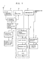
- reference numeral 16 is an intermediate frequency (IF) bandpass filter connected between the frequency converter 3 and the IF amplifier 4
- 17 is a frequency measuring means composed of counters the input of which is the output of phase-locked loop 6
- 18 is a frequency comparison means which comprises a sequence circuit composed of adders, latch circuits, and a reference frequency generator or a microprocessor and outputs a frequency error correction data in accordance with an output signal of the frequency measuring means 17
- 19 is a digital-to-analog converter (hereinafter abbreviated as D/A converter)
- D/A converter digital-to-analog converter
- 20 is a field intensity level detection circuit which detects the field intensity of the IF signal.
- Fig. 4 is a wave diagram of a received burst applied to the embodiments described above.
- the wave form includes a carrier reproducing portion 101 and a data portion 102 which are separated from each other.
- Fig. 5 is a block diagram showing examples of arrangements of the synchronous circuit 11, the control circuit 12, the frequency measuring means 17, and the frequency comparison means 18 in the embodiment described above.
- the synchronous circuit 11 comprises a binary correlator 117 and a magnitude comparator 118, the former having a sampler 111 for inputting demodulated data output from the demodulator 5, a comparator 112 for comparing an output signal of the sampler 111 with a reference signal, a reference register 113, a shift register 114, an exclusive OR circuit 115, and an adder 116.
- the control circuit 12 comprises an AND gate 121 which obtains the logical AND of the synchronous signal output from the magnitude comparator 118 and the output signal from the electric field level detection unit 20, a counter 122 which receives the output signal from the AND circuit 121, begins counting of the reference oscillation signal from the reference oscillator 13 until the time T1 shown in Fig. 4 elapses and a predetermined count number is reached, a counter 123 which receives the count up signal from the counter 122, begins counting of the reference signal from the reference oscillator 13 until the time T2 shown in Fig. 4 elapses and a predetermined count number is reached, and a flip-flop 124 which is reset by the count up signal of the counter 122 and set by the count up signal of the counter 122 to output a control signal.
- the count up signal of the counter 12 brings the through/hold circuit 9 into a through state, and at the same time, makes the frequency measuring means 17 stop the measuring operation, and the count up signal of the counter 123 brings the through/hold circuit 9 into a hold state, and at the same time, makes the frequency measuring means 17 start the measuring operation.
- the frequency measuring means 17 and the frequency comparison means 18 comprise a gate time generation circuit 171 which has been supplied with the reference oscillation signal from the reference oscillator 13 and starts its operation upon the reception of the control signal from control circuit 12 and a down counter 172 which starts its operation upon the reception of the control signal, subtracts the held frequency signal from the phase-locked loop until it receives gate signal from the gate time generation circuit 171, and outputs frequency correction data.
- the frequency is measured by the frequency measuring means 17.
- the result of frequency measurement thus obtained is sent to the frequency comparison means 18 and compared with an IF reference data preset in a memory in the frequency comparison means 18 which, as one example, may be 10.7 MHz, by which a correction data corresponding to the frequency difference between them is output.
- the frequency comparison means 18 outputs an initial value of a frequency correction data at step ST1.
- the means 18 waits until an oscillation frequency of the receiving local oscillator 14 becomes stable (Step ST2) and decides whether holding starts or not (Step ST3).
- the means 18 measures the held frequency (Step ST4) and decides whether the difference between the measured frequency data and the reference frequency data is within a fixed value or not (Step ST5), and in the case of NO, the means 18 outputs a frequency correction data and returns to the Step ST2 (Step ST6).
- the reference oscillator 13 is controlled to follow the received frequency, and consequently, an IF frequency becomes constant, and at the same time, the oscillation frequency of the transmitting carrier wave oscillator becomes stable.
- An electric field detector 20 monitors a received electric field level, and disables the control circuit 12 when the received field level is low by sending a logical "0" to AND circuit 121 shown in Fig. 5. As a result, when the received electric field level is low, the reference oscillator 13 cannot be controlled and the previous reference oscillation frequency is used as it is.
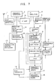
- Fig. 7 shows an example in which a narrow bandpass filter 21 is provided on the input side of the phase-locked loop 6 in the constitution in Fig. 3 described above.
- This constitution allows the sensitivity in a weak electric field to be raised, and, the automatic frequency control to be effectively done even in the case of a weak antenna input.
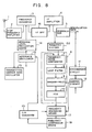
- Fig. 8 shows an example in which a frequency divider 22 is provided ont he input side of the phase-locked loop 6 in the constitution in Fig. 3 described above. This constitution divides the IF down to a frequency which is easy to process to sample the IF frequency, allowing it to be input to the phase-locked loop 6.
- FIG. 9 shows a constitution of a double superheterodyne receiving unit having two IFs, which is provided with a first IF generating unit 23-1 comprising a first frequency converter 3-1, a first IF amplifier 4-1, a first IF BPF 16-1, and a first receiving local oscillator 14-1 and a second IF generating unit 23-2 comprising a second frequency converter 3-2, a second IF BPF 16-1, a seocnd IF amplifier 4-2, and a second receiving local oscillator 14-2.
- the double superheterodyne receiving unit can make the two IF frequencies constant by controlling the first and second receiving local oscillators 14-1 and 14-2 by using the output of the reference oscillator 13.
- Fig. 10 is a block diagram showing a constitution of a receiving unit provided with an automatic frequency control device using a costas loop, and the same parts as those in Fig. 2 are identified by the same reference numerals to omit duplicated description.
- Fig. 10 refernece numeral 24-1 denotes a first multiplier, 24-2 a second multiplier, 25-1 a first lowpass filter (LPF), 25-2 a second lowpass filter (LPF), 24-3 a third multiplier, 24-4 a fourth multiplier, 26 a clock regenerative circuit, and 27 a 90° phase shifter.
- LPF lowpass filter
- LPF lowpass filter
- LPF lowpass filter
- 24-3 a third multiplier
- 24-4 a fourth multiplier
- 26 a clock regenerative circuit
- 27 a 90° phase shifter
- Fig. 11 is a block diagram showing a concrete constitution of the clock reproducing circuit 26 of Fig. 10.
- the clock reproducing circuit 26 comprises a variable frequency divider 261 which divides the frequency of the refernece oscillation signal from the reference oscillator 13, a fixed frequency divider 262 which divides the frequency of an output signal of the variable frequency divider 261 and outputs a reproduced clock, a phase comparator 263 which compares a phase of an output signal of a multiplier 265 with the phase of the reproduced clock.
- Multiplier 265 outputs a signal equal to the product of the in-phase component I and the orthogonal component Q of the demodulated data.
- An up/down counter 264 receives an output signal of the multiplier (265(?) at its clock terminal and an output signal of the phase comparator 263 is inputted to its up/down terminal to perform up/down counting and the counted result is fed back to the variable frequency divider 261, thereby performing control so as to make the phase of the output signal of the multiplier 24-1 coincide with that of the reproduced clock.
- the first lowpass filter 25-1 filters the output of the first multiplier 24-1 and outputs the following signal. 1 ⁇ 2 ⁇ I(t)cos ⁇ t - 1 ⁇ 2 ⁇ Q(t)sin ⁇ t
- the second multiplier 24-2 receives the output signal of the IF amplifier 4 and the output signal of the 90° phase shifter 27, which represents a 90° phase shifted VCO signal , and performs the following operation.
- the second lowpass filter 25-2 filters the output signal of the second multiplier 24-2 and outputs the following signal. 1 ⁇ 2 I(t)sin ⁇ t + 1 ⁇ 2 Q(t)cos ⁇ t
- the third multiplier 24-3 multiplies the output of the first lowpass filter 25-1, and the output of the second lowpass filter 25-2.
- the output signal of the fourth multiplier 24-4 is fed back via the loop filter 8 and the through/hold circuit 9 in a through state to the VCO 10, and the received carrier wave frequency retained in the VCO 10 is measured by the frequency measuring means 17 when the through/hold circuit 9 is in a hold state.
- the result of this frequency measurement is compared with the preset frequency reference data by the frequency caparison means 18, and the frequency correction data corresponding to the difference frequency is converted into an analog signal by the D/A converter 19. Then, the analog signal is supplied to the reference oscillator 13 to control the reference oscillator 13 to follow the received carrier frequency.
- a receiving frequency is stored and held, the held receiving frequency is measured to compare it with the preset frequency reference, and the reference oscillator is controlled in response to the frequency correction data corresponding to the difference between the preset frequency and the held receiving frequency. Accordingly, the IF can be made constant without the use of an expensive reference oscillator, and the oscillation frequency of the transmitting carrier oscillator is stabilized.
Landscapes
- Stabilization Of Oscillater, Synchronisation, Frequency Synthesizers (AREA)
- Channel Selection Circuits, Automatic Tuning Circuits (AREA)
- Digital Transmission Methods That Use Modulated Carrier Waves (AREA)
- Superheterodyne Receivers (AREA)
Applications Claiming Priority (2)
| Application Number | Priority Date | Filing Date | Title |
|---|---|---|---|
| JP207348/89 | 1989-08-10 | ||
| JP1207348A JPH07105822B2 (ja) | 1989-08-10 | 1989-08-10 | 自動周波数制御装置 |
Publications (2)
| Publication Number | Publication Date |
|---|---|
| EP0412207A1 true EP0412207A1 (fr) | 1991-02-13 |
| EP0412207B1 EP0412207B1 (fr) | 1994-07-20 |
Family
ID=16538250
Family Applications (1)
| Application Number | Title | Priority Date | Filing Date |
|---|---|---|---|
| EP89122976A Expired - Lifetime EP0412207B1 (fr) | 1989-08-10 | 1989-12-13 | Commande automatique de fréquence |
Country Status (5)
| Country | Link |
|---|---|
| US (1) | US5574998A (fr) |
| EP (1) | EP0412207B1 (fr) |
| JP (1) | JPH07105822B2 (fr) |
| DE (1) | DE68916952T2 (fr) |
| NO (1) | NO175128C (fr) |
Cited By (7)
| Publication number | Priority date | Publication date | Assignee | Title |
|---|---|---|---|---|
| EP0521403A1 (fr) * | 1991-06-29 | 1993-01-07 | Nec Corporation | Récepteur de radio avec suppression du glissement de la fréquence intermédiaire |
| EP0527481A1 (fr) * | 1991-08-12 | 1993-02-17 | Fujitsu Limited | Circuit convertisseur de fréquence |
| EP0457542A3 (en) * | 1990-05-17 | 1993-03-03 | Sony Corporation | Transceiver with doppler correction |
| EP0545342A1 (fr) * | 1991-12-02 | 1993-06-09 | Sony Corporation | Récepteur superhétérodyne |
| EP0580294A3 (fr) * | 1992-06-23 | 1994-03-30 | Japan Radio Co Ltd | |
| EP0833448A3 (fr) * | 1996-09-27 | 1998-06-10 | Nec Corporation | Méthode et circuit d'ajustement de fréquence dans un récepteur numérique |
| EP1480354A3 (fr) * | 2003-05-23 | 2006-07-26 | Gilat Satellite Networks Ltd. | Synchronisation en fréquence et temporelle et correction d'erreur dans un réseau satellitaire |
Families Citing this family (14)
| Publication number | Priority date | Publication date | Assignee | Title |
|---|---|---|---|---|
| JP3179344B2 (ja) * | 1996-06-28 | 2001-06-25 | 静岡日本電気株式会社 | 無線通信端末における自動周波数補正方法及び通信制御方法 |
| JPH1098354A (ja) * | 1996-09-24 | 1998-04-14 | Matsushita Electric Ind Co Ltd | 自動周波数制御回路 |
| KR100233658B1 (ko) * | 1996-10-21 | 1999-12-01 | 윤종용 | 고선명 텔레비젼 수신기의 반송파 복구시간을 줄이는 방법 |
| JP2880971B2 (ja) * | 1996-11-15 | 1999-04-12 | 埼玉日本電気株式会社 | 周波数安定化回路 |
| JP3226807B2 (ja) | 1996-11-20 | 2001-11-05 | 静岡日本電気株式会社 | 無線呼出システム用の自動周波数補正装置および自動周波数補正方法 |
| JP3397238B2 (ja) * | 1998-10-01 | 2003-04-14 | 日本電気株式会社 | 移動局および移動局におけるafc制御方法 |
| AU7834700A (en) | 1999-09-27 | 2001-04-30 | Parthus Technologies Plc | Method and apparatus for a frequency synthesizer having a compensated sigma delta modulator output signal |
| CA2352398C (fr) * | 2000-07-06 | 2005-07-26 | Unique Broadband Systems, Inc. | Convertisseur de frequence de bruit de phase faible |
| JP3599183B2 (ja) * | 2001-03-28 | 2004-12-08 | 日本電気株式会社 | 衛星通信送信制御方式及び小型地球局 |
| JP4325490B2 (ja) * | 2004-06-10 | 2009-09-02 | 株式会社デンソー | ヘテロダイン受信機 |
| DE102005010982A1 (de) * | 2005-03-03 | 2006-09-07 | Bizerba Gmbh & Co. Kg | Kraftmesszelle |
| WO2007004465A1 (fr) * | 2005-07-04 | 2007-01-11 | Matsushita Electric Industrial Co., Ltd. | Dispositif semi-conducteur et dispositif à circuit radio utilisant ledit dispositif |
| JP4855846B2 (ja) * | 2006-06-27 | 2012-01-18 | 日本無線株式会社 | ディジタル復調装置 |
| FR3016102A1 (fr) * | 2013-12-31 | 2015-07-03 | Commissariat Energie Atomique | Circuit de reception radiofrequence a tres basse consommation |
Citations (3)
| Publication number | Priority date | Publication date | Assignee | Title |
|---|---|---|---|---|
| EP0044374A1 (fr) * | 1980-07-22 | 1982-01-27 | Robert Bosch Gmbh | Procédé de synchronisation en fréquence d'un oscillateur libre, commandé par tension d'un circuit à boucle d'asservissement de phase dans un récepteur radio |
| EP0253680A2 (fr) * | 1986-07-18 | 1988-01-20 | Nippon Telegraph And Telephone Corporation | Appareil de réception de signaux modulés en angle |
| DE3738124A1 (de) * | 1986-12-01 | 1988-06-16 | Nokia Mobira Oy | Eine die traegerwelle des fm-synthesators fuer ein telefonsystem steuernde schaltung |
Family Cites Families (6)
| Publication number | Priority date | Publication date | Assignee | Title |
|---|---|---|---|---|
| US4715001A (en) * | 1984-08-23 | 1987-12-22 | Motorola, Inc. | Extremely accurate automatic frequency control circuit and method therefor |
| JPS6173416A (ja) * | 1984-09-19 | 1986-04-15 | Nec Corp | 自動周波数制御・自動利得制御回路 |
| US4703520A (en) * | 1986-10-31 | 1987-10-27 | Motorola, Inc. | Radio transceiver having an adaptive reference oscillator |
| JPH0744485B2 (ja) * | 1987-05-22 | 1995-05-15 | 三菱電機株式会社 | 自動車電話装置 |
| JPH01128624A (ja) * | 1987-11-13 | 1989-05-22 | Nippon Telegr & Teleph Corp <Ntt> | 周波数安定化機能を有する移動無線機 |
| SE460086B (sv) * | 1987-11-27 | 1989-09-04 | Ericsson Telefon Ab L M | Anordning foer korrigering av frekvensen i en koherent mottagare |
-
1989
- 1989-08-10 JP JP1207348A patent/JPH07105822B2/ja not_active Expired - Lifetime
- 1989-12-06 US US07/446,805 patent/US5574998A/en not_active Expired - Lifetime
- 1989-12-08 NO NO894947A patent/NO175128C/no not_active IP Right Cessation
- 1989-12-13 EP EP89122976A patent/EP0412207B1/fr not_active Expired - Lifetime
- 1989-12-13 DE DE68916952T patent/DE68916952T2/de not_active Expired - Lifetime
Patent Citations (3)
| Publication number | Priority date | Publication date | Assignee | Title |
|---|---|---|---|---|
| EP0044374A1 (fr) * | 1980-07-22 | 1982-01-27 | Robert Bosch Gmbh | Procédé de synchronisation en fréquence d'un oscillateur libre, commandé par tension d'un circuit à boucle d'asservissement de phase dans un récepteur radio |
| EP0253680A2 (fr) * | 1986-07-18 | 1988-01-20 | Nippon Telegraph And Telephone Corporation | Appareil de réception de signaux modulés en angle |
| DE3738124A1 (de) * | 1986-12-01 | 1988-06-16 | Nokia Mobira Oy | Eine die traegerwelle des fm-synthesators fuer ein telefonsystem steuernde schaltung |
Cited By (21)
| Publication number | Priority date | Publication date | Assignee | Title |
|---|---|---|---|---|
| EP0457542A3 (en) * | 1990-05-17 | 1993-03-03 | Sony Corporation | Transceiver with doppler correction |
| US5261120A (en) * | 1990-05-17 | 1993-11-09 | Sony Corporation | Method and apparatus for transmitting a signal with an offset which follows a received signal |
| EP0521403A1 (fr) * | 1991-06-29 | 1993-01-07 | Nec Corporation | Récepteur de radio avec suppression du glissement de la fréquence intermédiaire |
| US5542114A (en) * | 1991-06-29 | 1996-07-30 | Nec Corporation | Radio receiver for suppressing frequency drift in an intermediate frequency stage |
| AU654193B2 (en) * | 1991-06-29 | 1994-10-27 | Nec Corporation | Radio receiver capable of suppressing a frequency drift in an intermediate frequency |
| EP0527481A1 (fr) * | 1991-08-12 | 1993-02-17 | Fujitsu Limited | Circuit convertisseur de fréquence |
| US5388125A (en) * | 1991-08-12 | 1995-02-07 | Fujitsu Limited | Frequency converter circuit with improved intermediate frequency stability |
| EP0545342A1 (fr) * | 1991-12-02 | 1993-06-09 | Sony Corporation | Récepteur superhétérodyne |
| US5361407A (en) * | 1991-12-02 | 1994-11-01 | Sony Corporation | Double superheterodyne receiver with independent frequency calibration of two local oscillators |
| EP0662754A1 (fr) * | 1992-06-23 | 1995-07-12 | Japan Radio Co., Ltd | Circuit de commande automatique de fréquence |
| AU659018B2 (en) * | 1992-06-23 | 1995-05-04 | Japan Radio Co., Ltd. | Automatic frequency control circuit |
| EP0663725A1 (fr) * | 1992-06-23 | 1995-07-19 | Japan Radio Co., Ltd | Circuit de commande automatique de fréquence |
| US5513388A (en) * | 1992-06-23 | 1996-04-30 | Japan Radio Co., Ltd. | Automatic frequency control circuit |
| EP0580294A3 (fr) * | 1992-06-23 | 1994-03-30 | Japan Radio Co Ltd | |
| AU670896B2 (en) * | 1992-06-23 | 1996-08-01 | Japan Radio Co., Ltd. | Automatic frequency control circuit |
| AU671570B2 (en) * | 1992-06-23 | 1996-08-29 | Japan Radio Co., Ltd. | Automatic frequency control circuit |
| EP0833448A3 (fr) * | 1996-09-27 | 1998-06-10 | Nec Corporation | Méthode et circuit d'ajustement de fréquence dans un récepteur numérique |
| US6052419A (en) * | 1996-09-27 | 2000-04-18 | Nec Corporation | Frequency adjusting method for use with digital receiver and frequency adjusting circuit thereof |
| EP1480354A3 (fr) * | 2003-05-23 | 2006-07-26 | Gilat Satellite Networks Ltd. | Synchronisation en fréquence et temporelle et correction d'erreur dans un réseau satellitaire |
| US7471720B2 (en) | 2003-05-23 | 2008-12-30 | Gilat Satellite Networks, Inc. | Frequency and timing synchronization and error correction in a satellite network |
| EP2472736A1 (fr) * | 2003-05-23 | 2012-07-04 | Gilat Satellite Networks Ltd. | Synchronisation de la fréquence et du temps et correction d'erreurs dans un réseau satellite |
Also Published As
| Publication number | Publication date |
|---|---|
| JPH0370335A (ja) | 1991-03-26 |
| EP0412207B1 (fr) | 1994-07-20 |
| NO175128C (no) | 1994-08-31 |
| US5574998A (en) | 1996-11-12 |
| DE68916952T2 (de) | 1995-03-09 |
| NO894947D0 (no) | 1989-12-08 |
| DE68916952D1 (de) | 1994-08-25 |
| JPH07105822B2 (ja) | 1995-11-13 |
| NO175128B (no) | 1994-05-24 |
| NO894947L (no) | 1991-02-11 |
Similar Documents
| Publication | Publication Date | Title |
|---|---|---|
| US5574998A (en) | Automatic frequency control circuit for control of reference oscillator in communication apparatus | |
| EP0441593B1 (fr) | Circuit de contrÔle de fréquence automatique | |
| US6195400B1 (en) | Two-mode demodulating apparatus | |
| JP2744644B2 (ja) | 拡散スペクトル受信機における遅延ロックループ回路 | |
| JPH0583313A (ja) | 復調回路 | |
| US5703527A (en) | Frequency modulated signal demodulator circuit and communication terminal equipment | |
| JPH0548483A (ja) | 周波数変換回路 | |
| JP2932861B2 (ja) | 位相同期検出回路 | |
| EP0373517B1 (fr) | Commande de fréquence automatique numérique pour ondes sinusoidales pures | |
| JP3898839B2 (ja) | 送信機 | |
| JP3254009B2 (ja) | 位相固定ループを含む回路 | |
| JPS644386B2 (fr) | ||
| JPH07143199A (ja) | ディジタル信号復調装置 | |
| JPH06326740A (ja) | 移動無線機 | |
| JP3434301B2 (ja) | タイミング抽出方法及びタイミング抽出回路 | |
| JPH09326752A (ja) | 移動体通信端末装置 | |
| JP3396047B2 (ja) | 受信装置 | |
| JP3462277B2 (ja) | 搬送波再生回路 | |
| JPS6089155A (ja) | 位相同期方式 | |
| JP3519365B2 (ja) | エネルギ分散されたqpsk信号の搬送波に対する簡単な同期化の支援のための方法 | |
| JP2650557B2 (ja) | 同期型スペクトル拡散変調波の復調装置 | |
| JPH02100510A (ja) | 自動周波数制御装置 | |
| JPH07273821A (ja) | 復調装置 | |
| JPH06177921A (ja) | ディジタル信号復調回路 | |
| JPH0654013A (ja) | 受信機の周波数変換回路 |
Legal Events
| Date | Code | Title | Description |
|---|---|---|---|
| PUAI | Public reference made under article 153(3) epc to a published international application that has entered the european phase |
Free format text: ORIGINAL CODE: 0009012 |
|
| 17P | Request for examination filed |
Effective date: 19901213 |
|
| AK | Designated contracting states |
Kind code of ref document: A1 Designated state(s): DE FR GB SE |
|
| 17Q | First examination report despatched |
Effective date: 19930601 |
|
| GRAA | (expected) grant |
Free format text: ORIGINAL CODE: 0009210 |
|
| AK | Designated contracting states |
Kind code of ref document: B1 Designated state(s): DE FR GB SE |
|
| REF | Corresponds to: |
Ref document number: 68916952 Country of ref document: DE Date of ref document: 19940825 |
|
| ET | Fr: translation filed | ||
| EAL | Se: european patent in force in sweden |
Ref document number: 89122976.7 |
|
| PLBE | No opposition filed within time limit |
Free format text: ORIGINAL CODE: 0009261 |
|
| STAA | Information on the status of an ep patent application or granted ep patent |
Free format text: STATUS: NO OPPOSITION FILED WITHIN TIME LIMIT |
|
| 26N | No opposition filed | ||
| REG | Reference to a national code |
Ref country code: GB Ref legal event code: 746 Effective date: 19951106 |
|
| REG | Reference to a national code |
Ref country code: FR Ref legal event code: D6 |
|
| REG | Reference to a national code |
Ref country code: GB Ref legal event code: IF02 |
|
| PGFP | Annual fee paid to national office [announced via postgrant information from national office to epo] |
Ref country code: SE Payment date: 20081205 Year of fee payment: 20 |
|
| PGFP | Annual fee paid to national office [announced via postgrant information from national office to epo] |
Ref country code: DE Payment date: 20081211 Year of fee payment: 20 |
|
| PGFP | Annual fee paid to national office [announced via postgrant information from national office to epo] |
Ref country code: GB Payment date: 20081210 Year of fee payment: 20 |
|
| REG | Reference to a national code |
Ref country code: GB Ref legal event code: PE20 Expiry date: 20091212 |
|
| PG25 | Lapsed in a contracting state [announced via postgrant information from national office to epo] |
Ref country code: GB Free format text: LAPSE BECAUSE OF EXPIRATION OF PROTECTION Effective date: 20091212 |
|
| PGFP | Annual fee paid to national office [announced via postgrant information from national office to epo] |
Ref country code: FR Payment date: 20081212 Year of fee payment: 20 |