EP0412267A2 - Interface de données asynchrone à grande vitesse - Google Patents
Interface de données asynchrone à grande vitesse Download PDFInfo
- Publication number
- EP0412267A2 EP0412267A2 EP90111930A EP90111930A EP0412267A2 EP 0412267 A2 EP0412267 A2 EP 0412267A2 EP 90111930 A EP90111930 A EP 90111930A EP 90111930 A EP90111930 A EP 90111930A EP 0412267 A2 EP0412267 A2 EP 0412267A2
- Authority
- EP
- European Patent Office
- Prior art keywords
- buffer
- data
- frame
- register
- clock
- Prior art date
- Legal status (The legal status is an assumption and is not a legal conclusion. Google has not performed a legal analysis and makes no representation as to the accuracy of the status listed.)
- Granted
Links
Images






Classifications
-
- G—PHYSICS
- G06—COMPUTING OR CALCULATING; COUNTING
- G06F—ELECTRIC DIGITAL DATA PROCESSING
- G06F5/00—Methods or arrangements for data conversion without changing the order or content of the data handled
- G06F5/06—Methods or arrangements for data conversion without changing the order or content of the data handled for changing the speed of data flow, i.e. speed regularising or timing, e.g. delay lines, FIFO buffers; over- or underrun control therefor
- G06F5/16—Multiplexed systems, i.e. using two or more similar devices which are alternately accessed for enqueue and dequeue operations, e.g. ping-pong buffers
Definitions
- This invention relates to an asynchronous high-speed data interface for processing serial data frames and, more particularly, to such an interface for processing frames originating from a serial channel and destined for a control unit having a parallel interface.
- the total extended channel consists of a cooperating serial channel, associated with a host processor, which is connected through a serial fiber-optic link to an extender unit coupled to one or more parallel control units.
- the control units in turn handle devices, especially direct-access storage devices (DASD) such as magnetic disk drives.
- DASD direct-access storage devices
- the serial protocols for communicating over the fiber-optic link and the format of the serial frames transmitted over the link are also described in the above-identified copending application of D. F. Casper et al.
- the use of the serial fiber-optic link between the serial channel and the extender unit allows control units to be placed up to 3 km from the channel (1 km in the case of certain time-critical control units), as contrasted with a distance of about 400 feet for conventional parallel channels and control units.
- the channel and the extender unit coupled by the fiber-optic link are timed by clocks which, although having the same nominal frequency, run asynchronously with each other.
- frames arriving from the channel are received under the control of a clock that is synchronous with the channel transmitter clock and are later processed under the control of a clock that is used generally to time the extender unit logic and is asynchronous with the channel transmitter clock.
- Such asynchronism between the receiving of the serial frame and its later processing usually requires that the entire frame be received in an input buffer and checked for validity before the frame is further processed. This requirement significantly limits the data transmission rate and may result in an input buffer overrun if two consecutive frames are spaced two closely together. Further, the necessity of receiving the entire frame in the input buffer before proceeding with later processing increases the effective latency period of the device connected to the control unit.
- a principal object of the present invention is to provide a data interface that handles data that is asynchronous with circuits that later process the data.
- a further object of the present invention is to provide a data interface that is capable of high-speed operation without data overrun.
- the present invention contemplates an asynchronous data interface for processing serial data frames, such as those originating from a serial channel, transmitted in synchronism with a first clock in which a first clocked logic circuit operating synchronously with the first clock fills an input buffer with data from the frames.
- a second clocked logic circuit operating synchronously with a second clock that is asynchronous with the first clock begins emptying data from the buffer before the first clocked logic circuit has completed its filling operation.
- the frames comprise a start-of-frame (SOF) delimiter (in particular a passive-start-of-frame (PSOF) delimiter), one or more data bytes, one or more cyclic redundancy check (CRC) bytes, and an end-of-frame (EOF) delimiter which may be either a normal disconnect-end-of-frame (DEOF) delimiter or an abort-end-of-frame (AEOF) delimiter.
- SOF start-of-frame
- PSOF passive-start-of-frame
- CRC cyclic redundancy check
- EEF end-of-frame
- the first clocked logic circuit begins to fill the input buffer in synchronism with the first clock upon detecting an SOF delimiter and, optionally, other non-data bytes such as an architecture identifier (AID) or the like.
- the first clocked logic circuit Upon detecting the receipt of a predetermined number of data bytes, preferably three, the first clocked logic circuit sets a start latch to signal the second clocked logic circuit to begin emptying the data bytes from the input buffer into an output buffer in synchronism with the second clock.
- the second clocked logic circuit uses a pointer register to address the output buffer. Upon detecting the setting of the start latch, and before initiating the transfer of data from the input buffer to the output buffer, the second clocked logic circuit stores the existing contents of the pointer register in a backup pointer register. As the second clocked logic circuit transfers successive data bytes from the input buffer to the output buffer, it increments a backup byte counter used to keep track of the number of bytes in the output buffer awaiting further processing.
- the backup byte counter is readable only by the second clocked logic circuit, and not by the logic circuit that further processes the data in the output buffer.
- the first clocked logic circuit Upon detecting the start of an EOF delimiter, the first clocked logic circuit performs a CRC check and sets a pause latch, signaling the second clocked logic circuit to halt temporarily the further transfer of data from the input buffer to .the output buffer. If the EOF delimiter is a normal EOF delimiter, and if the CRC check is satisfactory, the first clocked logic circuit sets a "good" latch, signaling the second logic circuit to complete the transfer of the frame data from the input buffer to the output buffer. On completion of the data transfer, the second clocked logic circuit transfers the contents of the backup byte counter to the principal byte counter that is readable by other logic circuitry.
- the first clocked logic circuit sets an abort latch, signaling the second clocked logic circuit to abort the transfer sequence.
- the second clocked logic circuit restores the contents of the backup pointer register to the principal pointer register, and does not transfer the contents of the backup byte counter to the principal counter.
- the present invention permits the transfer of contents from the input buffer to the output buffer before the incoming frame is completely received and checked for validity. By delaying the transfer from the input buffer until a predetermined number of incoming data bytes have been received, one ensures that the second clocked logic circuit will always have data in the input buffer to transfer to the output buffer while the input buffer is being filled.
- a system 10 incorporating the present invention includes a host processor 12, which communicates by way of a parallel bus (not separately shown) with a channel 14.
- Channel 14 in turn, communicates serially with a channel extender unit 22 by way of a duplex fiber-optic link 16 comprising an outbound conductor 18 for transmitting information from the channel 14 to the extender unit 22 and an inbound conductor 20 transmitting information back from the extender unit 22 to the channel 14.
- Extender unit 22 in turn communicates with one or more control units (CUs) 26 by way of a parallel interface 24 comprising bus and tag lines.
- the protocols governing the serial link communications between the channel 14 and the extender unit 22 are described in the copending application of D. F. Casper et al. referred to above.
- the serialized characters flowing on the serial link 16 are described in Franaszek et al. U.S. Patent 4,486,739.
- a normal frame conforming to the protocol referred to above consists of a two-character passive-start-of-frame (PSOF) delimiter, an architecture identifier (AID) character, from 1 to 130 frame contents characters, and two cyclic redundancy check (CRC) characters followed by a three-character disconnect-end-of-frame (DEOF) delimiter.
- PSOF passive-start-of-frame
- AID architecture identifier
- CRC cyclic redundancy check
- DEOF three-character disconnect-end-of-frame
- Data frames are variable in length, and contain from 1 to 16 data bytes, and are used to transfer data between the main storage (not shown) associated with the channel 14 and host processor 12 and the devices attached to control units 26.
- extender unit 22 contains a receiver/deserializer/decoder (RX/DESR/DEC) 28, hereinafter simply "decoder”, which converts serialized light pulses to electrical signals, accumulates successive groups of ten serial bits into ten-bit transmission code characters, and converts the ten-bit transmission code characters to eight-bit format characters containing bits 0 to 7, a "K" bit and an odd parity bit (P).
- the K bit is used to distinguish the special ten-bit transmission codes (K characters) used as idle characters, frame delimiters and special continuous sequences from data characters, as described in U.S. Patent No. 4,486,739, referred to above.
- a first clocked logic circuit detects the arrival of a frame from the channel 14 (Fig. 1), checks the frame including the CRC characters for validity and stores the frame in one of two dual-port buffers constituting the In-frame Buffers (IBs) 32.
- IBs In-frame Buffers
- a frame is considered arriving into extender unit 22 if an SOF delimiter is received, which usually occurs after receiving one or more idle characters.
- Each storage location of buffers 32 stores 9 bits, i.e. data bits 0-7 and the parity bit P; the K bit is not stored since it is always 0 for a data character.
- Each of the two dual-port buffers which together constitute IBs 32 is capable of holding 20 characters, which is sufficient for the maximum outbound frame contents of 18 characters plus 2 CRC characters.
- the CRC characters are written into IBs 32 since they cannot be recognized as CRC characters in advance of receiving the first K character of the DEOF delimiter. They are also used for logout purposes in case a CRC error is detected by IBFSM 30.
- a second clocked logic circuit controls the transfer of incoming data from the in-frame buffers 32 to storage means, more particularly, a pair of data buffers (DBs) indicated collectively by the reference number 44 and comprising a pair of individual buffers 44a and 44b (Fig 5).
- DBs data buffers
- INFRSM 34 also moves portions of the frame into a set of in-frame registers (INFRREGS) to decode the type of frame being processed.
- INFRSM 34 If it is a command frame, INFRSM 34 sends it to an Initial Selection State Machine (ISSM) 40 for execution.
- ISSM Initial Selection State Machine
- Microprocessor 38 is also responsible for reset and initialization sequences, error detection and reporting, and diagnostic controls.
- a Parallel Data Transfer State Machine (PARDXSM) 46 operating under the supervisory control of ISSM 40, controls the transfer of data from data buffers 44 to parallel interface 24 by way of NPL driver/receiver module (NPLD/R) 42.
- NPLD/R NPL driver/receiver module
- Module 42 converts the extender unit signal levels to those required to drive interface 24.
- PARDXSM 46 also controls the transfer of data in the other direction, from interface 24 through module 42 to data buffers 44, in the case of a read operation.
- An Out Frame State Machine (OUTFRSM) 48 controls the subsequent transfer of read data from data buffers 44 to an encoder/serializer/transmitter (TX/SER/ENC) 52, which encodes successive bytes into a suitable transmission format, converts the parallel bytes to serial form, and transmits the serial signal as light pulses on conductor 20 to channel 14 (Fig. 1).
- OUTFRSM 48 operates in conjunction with a set of out-frame registers (OUTFRREGS) 50.
- Decoder 28 and IBFSM 30 are timed by a Receive Byte Clock (RBC), internal to decoder 28, which uses the incoming signal from channel 14 (Fig. 1) to generate a clock that is synchronous with the channel transmitter clock.
- RBC Receive Byte Clock
- INFRSM 34, PARDXSM 46 and the other clocked logic circuits of extender unit 22 are timed by a Transmit Byte Clock (TBC) which, while having the same nominal frequency (e.g., 20 MHz) as the Receive Byte Clock (RBC), runs asynchronously relative thereto.
- TBC Transmit Byte Clock
- a fuller description of the general operation of the extender unit 22 may be found in the copending applications of D. F. Casper et al. and M. E. Carey et al. referred to above, which applications are incorporated herein by reference.
- input buffers 32 comprise a pair of dual-port buffers 32a (IB1) and 32b (IB2).
- a first port of each of buffers 32a and 32b receives parallel data inputs from an IBIN register (IBINREG) 54 contained in decoder 28.
- IBINREG 54 also supplies its output to a decoder 56 of IBFSM 30, which detects the presence of a K character as distinguished from a data character, the type of K character if present, and whether an AID character conforms to the protocol (i.e., is a hex '00').
- IBINREG 54 additionally supplies its output to a CRC generator/checker 58 contained in IBFSM 30, which performs a CRC check on the frame being received.
- the first ports of buffers 32a and 32b also receive write inputs from respective AND gates 60 and 62, each of which receives one input from a WRIB line of IBFSM 30.
- Gate 60 receives a second input from a complemented SELWRIB line from IBFSM 30, while gate 62 receives a second input from a SELWRIB line also originating from IBFSM 30.
- the first port of each of buffers 32a and 32b receives a write address input from an in-pointer register (IBINPTR) 154 of IBFSM 30.
- IBFSM 30 activates the WRIB line synchronously with the RBC clock to transfer a byte of incoming data from IBINREG 54 to the buffer 32a or 32b determined by the logic level of SELWRIB.
- IBFSM 30 also includes a pair of input buffer counters 158a and 158b (Fig. 3), which it uses to maintain respective counts IBINCTR1 and IBINCTR2 of the number of data bytes in input buffers 32a and 32b awaiting processing by INFRSM 34.
- IBFSM 30 contains various latches for communicating control signals across the asynchronous boundary dividing IBFSM 30 and INFRSM 34 (Fig. 2).
- IBFSM 30 contains a pair of RBCSTART latches 74, one for each of buffers 32a and 32b, a single RBCPAUSE latch 76, a pair of RBCGOOD latches 78, and a pair of RBCABORT latches 80.
- RBCSTART latches 74 one for each of buffers 32a and 32b
- RBCPAUSE latch 76 a single RBCPAUSE latch 76
- RBCGOOD latches 78 a pair of RBCGOOD latches 78
- RBCABORT latches 80 For simplicity of exposition, only a single latch of each of the paired latches 74, 78 and 80 is shown in Fig. 4.
- Latches 74-80 receive respective set inputs from lines 82, 86, 90 and 94 from IBFSM 30 and reset inputs from respective OR gates 100, 102, 104 and 106.
- OR gates 100-106 receive respective first inputs from lines 84, 88, 92 and 96 from IBFSM 30 and each receive a second input from a hardware reset (HWRST) line 98 originating from microprocessor 38 (Fig. 2).
- HWRST hardware reset
- Each of latches 74-80 in a manner well known in the art, comprises an input latch followed by an output latch and receives clocking signals from a pair of lines 108 (shown in Fig. 4 as a single line) originating from the Receive Byte Clock (RBC).
- the respective clocking signals supplied to latches 74-80 are so timed that, on each cycle of the Receive Byte Clock (RBC) the input latch half is loaded with the information appearing at the latch inputs, following which that information is transferred from the input latch half to the output latch half.
- INFRSM 34 contains a pair of TBCSTART latches 110, a single TBCPAUSE latch 112, a pair of TBCGOOD latches 114, and a pair of TBCABORT latches 116.
- latches 110, 114 and 116 although paired to correspond with respective buffers 32a and 32b, are each shown as only a single latch in Fig. 4.
- TBCPAUSE latch 112 is a polarity hold latch which, as shown in Fig. 4, receives its D-input directly from the output of RBCPAUSE latch 76. The output of latch 112 takes on the new value appearing at the D-input on each TBC clock cycle.
- Latches 110, 114 and 116 receive respective set inputs from OR gates 132, 136 and 140, each of which receives one input from the corresponding latch in IBFSM 30 and a second input from a line 118, 120 or 122 originating from the microprocessor 38. Lines 118-122 are used for diagnostic purposes only and are normally inactive. Likewise, latches 110, 114 and 116 receive respective reset inputs from OR gates 134, 138 and 142, each of which receives one input from HWRST line 98 and a second input from a line 124, 126 or 128 originating from INFRSM 34. Finally, each of latches 110-116 receives clocking signals from a pair of lines 130 (shown as a single line in Fig.
- latches 110-116 of INFRSM 34 each comprise an input latch half and an output latch half, which are consecutively triggered on each cycle of the Transmit Byte Clock (TBC).
- IBFSM 30 also includes a pair of RBCSTARTSYNC latches 152 corresponding respectively to input buffers 32a and 32b.
- Latches 152 are polarity hold latches, similar to TBCPAUSE latch 112, which receive clock inputs from RBC lines 108 and respective D-inputs from the corresponding IBSTART outputs of TBCSTART latches 110.
- IBFSM 30 uses latches 152 to determine, prior to filling a selected input buffer 32a or 32b with data from a frame, whether the buffer has been emptied of data from a previous frame by INFRSM 34.
- INFRSM 34 also contains an in-frame buffer output register (IBOUTREG) 72, which receives gated outputs from respective buffers 32a and 32b.
- IBOUTREG 72 receives data from the second port of buffer 32a by way of gate 64, while if SELRDIB is high, IBOUTREG 72 receives data from the second port of buffer 32b by way of gate 70.
- Respective gates 66 and 68 supply the second port of a selected buffer 32a or 32b with a RDIB signal generated by INFRSM 34 synchronously with the TBC clock, the selection depending on the logic level of the SELRDIB signal also generated by INFRSM 34.
- An input buffer out-pointer register (IBOUTPTR) 156 similar to in-pointer register 154 of IBFSM 30 is used by INFRSM 34 to address via the second port the location of the selected buffer 32a or 32b from which data is read.
- INFRSM 34 also includes a data buffer in-pointer register (DBINPTR) 144, which it uses to address the selected buffer 44a or 44b to transfer bytes thereto from IBOUTREG 72.
- DBINPTR 144 Associated with DBINPTR 144 is a backup pointer register (DBINPTRBU) 146.
- DBINPTRBU backup pointer register
- INFRSM 34 Upon receiving an IBSTART signal from the selected latch 110 (Fig. 4), INFRSM 34 transfers the existing contents of DBINPTR 144 to DBINPTRBU 146. In the event of a subsequent IBABORT signal from the selected TBCABORT latch 146 (Fig. 4), the previously saved contents are restored to register 144 from backup register 146. In this manner, in the event that an incoming frame is aborted, INFRSM 34 in effect disregards the existence of any bytes of the aborted frame that it has written into DB 44.
- DBINPTR data buffer in-pointer register
- a byte counter (BC) 148 and a backup byte counter (BCBU) 150 are used to keep track of the number of bytes in the corresponding buffer 44a or 44b awaiting processing by PARDXSM 46.
- INFRSM increments BCBU 150.
- PARDXSM decrements the BC 148 and BCBU 150 corresponding to that buffer.
- PARDXSM 46 also increments the selected BC 148 each time it transfers a byte of data to the selected buffer 44a or 44b from the parallel interface 24 during channel write operations.
- INFRSM 34 increments only the backup counter 150 as it is transferring data from the selected buffer 32a or 32b to the selected buffer 44a or 44b.
- INFRSM 34 transfers the byte count from the selected backup counter 150 to the selected counter 148.
- INFRSM 34 restores the byte count from the end of the previous frame from counter 148 to backup counter 150.
- INFRSM 34 in effect masks the byte count for the selected buffer 44a or 44b from PARDXSM 46 until INFRSM has established that the incoming frame is good.
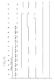
- IBFSM 30 for a valid write data frame will now be described, with particular reference to Figs. 7 and 9.
- IBFSM 30 Normally, when incoming line 18 from channel 14 carries idle (K28.5) characters, IBFSM 30 remains in state 0. While in this state IBFSM 30 continually enters a loop in which it examines the output of IBINREG 54 by way of decoder 56 for a start of frame (SOF) delimiter consisting of a K28.5 character ("SOF.5" in Figs. 7 and 9) followed by a K28.7 character ("SOF.7" in Figs. 7 and 9).
- SOF start of frame
- IBFSM 30 Upon receiving such a succession of K characters, and if the selected start as indicated by the selected RBCSTARTSYNC latch 152 is inactive, IBFSM 30 enters state 1. If at this time the selected RBCSTARTSYNC latch 152 is active, IBFSM 30 sets an "overrun pending" error condition, since INFRSM 34 has not finished processing data from the selected input buffer 32a or 32b.
- IBFSM 30 Upon entering state 1, IBFSM 30 monitors IBINREG for either the correct AID character (in this particular example a hex '00') or the first character K28.6 ("EOF.6" in Fig. 9) of an AEOF delimiter; detection of any other character will set a pending error condition. If such an AID character is received, IBFSM then enters state 2 (Fig. 9) to start the normal data-handling loop for writing incoming data into the selected input buffer 32a or 32b. On entering state 2, IBFSM 30 begins writing the incoming data bytes into the selected buffer 32a or 32b of IB 32, one byte per RBC clock cycle, beginning with the first data byte following the AID character.
- AID character in this particular example a hex '00'
- K28.6 in Fig. 9
- IBFSM 30 Upon entering state 1, IBFSM 30 monitors IBINREG for either the correct AID character (in this particular example a hex '00'
- IBFSM 30 increments IBINPTR 154 each time it writes a data byte into the selected input buffer 32a or 32b. IBFSM 30 also cycles each data byte through the CRC checker 58. Upon receiving the third such byte following the AID character, IBFSM 30 sets the selected RBCSTART latch 74 (Fig. 4). This results in the setting of the corresponding TBCSTART latch 110 on the next TBC clock cycle. The selected IBSTART signal generated by the selected TBCSTART latch 110 tells INFRSM 34 to begin transferring data from the selected input buffer 32a or 32b to the selected output buffer 44a or 44b, one byte at a time in synchronism with the TBC clock. Also at this time, IBFSM 30 begins incrementing the selected counter 158a or 158b for each byte transferred from IBINREG 54 to the selected buffer 32a or 32b.
- IBFSM 30 delays incrementing the selected counter 158a or 158b until the transfer of the third data byte to the selected register 32a or 32b because, as noted above, the two terminal CRC characters appear to be data bytes and are not recognized as CRC characters until the following K28.6 character of an EOF delimiter is detected. Ignoring the first two data characters compensates the byte count for the two CRC characters necessarily included in the count. As a result, INFRSM 34, which bases its actions on the contents of the selected counter 158a or 158b, will not transfer the CRC characters from the selected input buffer 32a or 32b to the selected data buffer, even though the CRC characters have been loaded into the input buffer.
- IBFSM 30 continues to fill the selected buffer of DB 32 with bytes from IBINREG 54 and to increment IBINPTR 154 and the selected counter 158a (IBINCTR1) or 158b (IBINCTR2) in this fashion until it detects the reception of a K28.6 character, which indicates the beginning of either a disconnect-end-of-frame (DEOF) delimiter (K28.6-K28.1-K28.1) or an abort-end-of-frame (AEOF) delimiter (K28.6-K28.4-K28.4).
- DEOF disconnect-end-of-frame
- AEOF abort-end-of-frame
- IBFSM 30 sets the RBCPAUSE latch 76 (Fig. 4). This results in the setting of the TBCPAUSE latch 112 on the next TBC clock cycle.
- the IBPAUSE signal generated by TBCPAUSE latch 112 tells INFRSM 34 to halt the further transfer of data from IB 32 to DB 44.
- IBFSM 30 also stops writing data into the selected buffer 32a or 32b and transitions to state 3. While in state 3, IBFSM 30 expects either a K28.1 character ("EOF.1" in Fig. 9) or a K28.4 character ("EOF.4" in Fig. 9) from IBINREG 54 of decoder 28. Detection of a K28.1 character indicates that a DEOF delimiter is being received, and IBFSM 30 transitions to state 4.
- IBFSM 30 monitors IBINREG 54 of decoder 28 for another K28.1 character. Detection of the second K28.1 character indicates the completion of a valid DEOF delimiter, causing IBFSM 30 to reset the selected RBCSTART latch 74 (Fig. 4), verify that the CRC check as indicated by circuit 58 (Fig. 3) is correct, set the selected RBCGOOD latch 78 (and thus the selected IBGOOD signal on the next TBC clock cycle) if the CRC check is good, toggle its SELWRIB pointer (Fig. 3), and transition to state 5.
- RBCGOOD latch 78 signals INFRSM 34 that the latter may continue with processing the frame and may regard it as a valid frame for the purpose of updating the registers and counters shown in Figs. 5 and 6. If the CRC check had not been good, the selected RBCGOOD latch would not have been set, and a CRC error condition would be set instead. In response this error condition, or any other error condition, microprocessor 38 generates a logout and resets the state machines and associated latches by pulsing HWRST line 98.
- IBFSM 30 While in state 5, IBFSM 30 expects either a K28.5 (idle) character or the first character (K28.6) of an AEOF delimiter. Upon detecting a K28.5 character, IBFSM 30 resets the RBCPAUSE latch 76 (and thus the IBPAUSE signal on the next TBC clock cycle) and returns to the idle state (state 0).
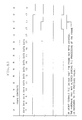
- IBFSM 30 assumed the reception of a valid write data frame terminated by a normal DEOF delimiter. If while in state 3, IBFSM 30 had detected a K28.4 character, indicating an AEOF delimiter rather than an DEOF delimiter, IBFSM 30 would transition to state 7, as shown in Fig. 8, instead of state 4. While in state 7, IBFSM 30 would monitor the output of IBINREG 54 of decoder 28 for another K28.4 character. Detection of the second K28.4 character completes a valid AEOF delimiter and causes IBFSM 30 to reset the selected RBCSTART latch 74.
- IBFSM 30 sets the selected RBCABORT latch 80, toggles the SELWRIB pointer, resets any pending error condition and transitions to state 5. Once it reaches state 5, IBFSM 30 functions in the manner described above for a valid write data frame.
- IBFSM 30 transitions to state 6 if it detects a K28.6 character while in state 0 or state 1, or while in state 2 if the selected RBCSTARTSYNC latch 152 is inactive. IBFSM 30 also transitions to state 6 after resetting the RBCPAUSE latch 76 if it detects a K28.6 character while in state 5. While in state 6, IBFSM monitors IBINREG 54 of decoder 28 for a K28.4 character. Detection of such a character indicates that an AEOF delimiter is being received. IBFSM 30 resets the selected RBCGOOD and RBCABORT latches 78 and 80 and transitions to state 7, at which point it operates in the manner described above.
- Latches 74-80 are the means by which IBFSM 30 communicates with INFRSM 34 across the asynchronous interface between the circuitry controlled by the Receive Byte Clock (RBC) and that controlled by the Transmit Byte Clock (TBC).
- RBC Receive Byte Clock
- TBC Transmit Byte Clock
- Each of RBC latches 74-80, when set, is set to remain on for at least two RBC clock cycles to ensure that at least one complete asynchronous TBC clock cycle is encompassed. This ensures that INFRSM 34 detects the setting of the RBC latch.
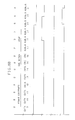
- INFRSM 34 for a valid write data frame will now be described with reference to Figs. 7 and 10.
- INFRSM 34 loops in its own state 0, monitoring the asynchronous interface for an active IBSTART signal from the selected TBCSTART latch 110.
- INFRSM 34 reads the first data byte from the selected buffer 32a or 32b and sequences to state 1.
- INFRSM 34 transfers the contents of pointer register (DBINPTR) 144 (Fig. 5) to backup pointer register (DBINPTRBU) 146, so that the previous pointer position may be restored if the frame is ultimately aborted.
- DBINPTR pointer register
- DBINPTRBU backup pointer register
- INFRSM 34 updates an op/flags register (OPFLGSREG) of INFRREGS 36 and decodes the op/flags byte to determine the type of frame arriving from channel 14.
- OFLGSREG op/flags register
- the frame arriving from channel 14 will always be (1) a command frame, having a fixed length of six data characters; (2) a control frame, having a fixed length of three data characters; (3) a data frame having a variable length of 1-17 data characters as indicated by the selected counter 158a or 158b; or (4) a test frame having a length of 1-18 data characters as indicated by the selected counter 158a or 158b.
- INFRSM 34 monitors the asynchronous interface for an active IBPAUSE, IBGOOD, or IBABORT indication from IBFSM 30, the IBGOOD and IBABORT indications monitored being, of course, those for the selected buffer 32a or 32b.
- INFRSM 34 will read the next byte from the selected buffer 32a or 32b and sequence to the next state, which is determined by the frame type that is being executed. It will be assumed for the purpose of the following description that the incoming frame, as indicated by the op/flags byte, is a write data frame. Other types of frames, however, may be processed in a similar manner.
- INFRSM 34 enters state B or state D, depending on the contents of IBOUTPTR 156 and the selected IBINCTR 158a or 158b and the logic levels of IBPAUSE and IBGOOD. If both the selected IBPAUSE and the selected IBGOOD are inactive, or if the selected IBGOOD is active but IBOUTPTR does not equal IBINCTR, INFRSM 34 changes from state 1 to state B. As shown in Fig. 7, upon entering state B, INFRSM 34 begins to transfer data from the selected buffer 32a or 32b (Fig. 3) to the selected buffer 44a or 44b (Fig.
- INFRSM 34 constantly monitors the asynchronous interface (Fig. 4) for a signal from the IBPAUSE line or from the selected IBGOOD or IBABORT line. Upon detecting an IBPAUSE signal, INFRSM 34 temporarily halts the transfer of data from the selected buffer 32a or 32b to DB 44 and incrementing of the pointer IBOUTPTR, and awaits an IBGOOD or IBABORT signal from the selected TBC latch 114 or 116. Upon subsequently detecting an IBGOOD signal from the selected TBCGOOD latch 114 (Fig.
- INFRSM 34 compares IBOUTPTR with IBINCTR. If IBOUTPTR is less than IBINCTR, INFRSM 34 continues to transfer bytes from the selected buffer 32a or 32b to the selected buffer 44a or 44b, incrementing IBOUTPTR, DBINPTR 144 (Fig. 5) and the selected BCBU 150 (Fig. 6) as it does so. When, finally, IBOUTPTR equals IBINCTR, INFRSM 34 changes to state D, where it transfers the contents of the selected BCBU 150 (Fig. 6) to the selected BC 148 to reveal the new byte count to PARDXSM 46. INFRSM then toggles its SELRDIB pointer (Fig. 3) and resets the selected TBCSTART and TBCGOOD latches 110 and 114 (Fig. 4) before returning to the idle state (state 0).
- the incoming write data frame will contain a sufficient number of bytes that INFRSM 34 will transition to state B before transitioning to state D.
- IBOUTPTR will already be equal to IBINCTR when the selected IBGOOD latch is set.
- INFRSM 34 changes directly from state 1 to state D, without passing through state B as an intermediary state. Otherwise, the manner of operation is similar to that described above.
- INFRSM 34 will detect an IBABORT signal from the selected TBCABORT latch 116 (Fig. 4) as shown in Fig. 8, rather than an IBGOOD signal from the selected TBCGOOD latch 114 as shown in Fig. 7. In such a case, INFRSM 34 halts any further transfer of data from the selected input buffer 32a or 32b, if it has not already done so, and transitions to state C instead of state D. On entering state C, INFRSM 34 transfers the contents of the backup pointer register (DBINPTRBU) 146 to the principal pointer register (DBINPTR) 144 (Fig.
- DBINPTRBU backup pointer register
- DBINPTR principal pointer register
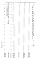
- the processing of a 16 byte write data frame is overlapped across the asynchronous interface, with the selected buffer 32a or 32b being emptied by INFRSM 34 while it is being filled with incoming data by IBFSM 30.
- the total processing period which begins with the reception of the initial K28.5 character of a PSOF delimiter and ends with the resetting of the TBC latches by INFRSM 34, spans 28 clock cycles.
- the total processing period would span 41 cycles if the processing by INFRSM 34 were to be delayed until IBFSM 30 had detected the final K28.1 character of the DEOF delimiter.
- the asynchronous data interface of the present invention finds special application in the channel extender unit described herein, it is not limited to use in such a unit, nor is it limited to systems using fiber-optic links. It could, for example, also be used in the serial channel itself for the reception of serial frames from the extender unit. More generally, the data interface of the present invention could be used in any application where there is the need to process incoming serial frames before they are completely received or checked for validity.
Landscapes
- Engineering & Computer Science (AREA)
- Theoretical Computer Science (AREA)
- Physics & Mathematics (AREA)
- General Engineering & Computer Science (AREA)
- General Physics & Mathematics (AREA)
- Communication Control (AREA)
- Information Transfer Systems (AREA)
Applications Claiming Priority (2)
| Application Number | Priority Date | Filing Date | Title |
|---|---|---|---|
| US392867 | 1989-08-11 | ||
| US07/392,867 US5133078A (en) | 1989-08-11 | 1989-08-11 | Serial frame processing system in which validation and transfer of a frame's data from input buffer to output buffer proceed concurrently |
Publications (3)
| Publication Number | Publication Date |
|---|---|
| EP0412267A2 true EP0412267A2 (fr) | 1991-02-13 |
| EP0412267A3 EP0412267A3 (en) | 1992-08-12 |
| EP0412267B1 EP0412267B1 (fr) | 1996-02-28 |
Family
ID=23552339
Family Applications (1)
| Application Number | Title | Priority Date | Filing Date |
|---|---|---|---|
| EP90111930A Expired - Lifetime EP0412267B1 (fr) | 1989-08-11 | 1990-06-23 | Interface de données asynchrone à grande vitesse |
Country Status (4)
| Country | Link |
|---|---|
| US (1) | US5133078A (fr) |
| EP (1) | EP0412267B1 (fr) |
| JP (1) | JPH0664564B2 (fr) |
| DE (1) | DE69025510T2 (fr) |
Cited By (3)
| Publication number | Priority date | Publication date | Assignee | Title |
|---|---|---|---|---|
| US5438575A (en) * | 1992-11-16 | 1995-08-01 | Ampex Corporation | Data storage system with stale data detector and method of operation |
| WO2001086409A3 (fr) * | 2000-05-08 | 2002-05-23 | Crossroads Sys Inc | Systeme et procede de commande de lecture de donnees de trame de tampon |
| GB2386714A (en) * | 2001-11-21 | 2003-09-24 | Nec Corp | Data transfer between processors using a system with an independent data transfer clock. |
Families Citing this family (16)
| Publication number | Priority date | Publication date | Assignee | Title |
|---|---|---|---|---|
| US5228129A (en) * | 1987-04-01 | 1993-07-13 | Digital Equipment Corporation | Synchronous communication interface for reducing the effect of data processor latency |
| US5444860A (en) * | 1992-02-14 | 1995-08-22 | Unisys Corporation | Translator system for message transfers between digital units operating on different message protocols and different clock rates |
| US5412782A (en) * | 1992-07-02 | 1995-05-02 | 3Com Corporation | Programmed I/O ethernet adapter with early interrupts for accelerating data transfer |
| US5434872A (en) * | 1992-07-28 | 1995-07-18 | 3Com Corporation | Apparatus for automatic initiation of data transmission |
| US5832310A (en) * | 1993-12-30 | 1998-11-03 | Unisys Corporation | Serial I/O channel having dependent and synchronous sources of control data and user defined data |
| US5553302A (en) * | 1993-12-30 | 1996-09-03 | Unisys Corporation | Serial I/O channel having independent and asynchronous facilities with sequence recognition, frame recognition, and frame receiving mechanism for receiving control and user defined data |
| US5463762A (en) * | 1993-12-30 | 1995-10-31 | Unisys Corporation | I/O subsystem with header and error detection code generation and checking |
| US5706443A (en) * | 1994-05-11 | 1998-01-06 | International Business Machines Corporation | Method and apparatus for enabling pipelining of buffered data |
| US5802307A (en) * | 1995-11-24 | 1998-09-01 | Sun Microsystems, Inc. | Network communications subsystem and method for digital computer system employing protocol stack having diverse lower-level network driver components optimized for each of base and enhance operating systems |
| US5898889A (en) * | 1996-04-30 | 1999-04-27 | 3Com Corporation | Qualified burst cache for transfer of data between disparate clock domains |
| US6092129A (en) * | 1998-04-13 | 2000-07-18 | Sandcraft, Inc. | Method and apparatus for communicating signals between circuits operating at different frequencies |
| US6643716B2 (en) * | 1999-03-29 | 2003-11-04 | Intel Corporation | Method and apparatus for processing serial data using a single receive fifo |
| US6381661B1 (en) * | 1999-05-28 | 2002-04-30 | 3Com Corporation | High throughput UART to DSP interface having Dual transmit and receive FIFO buffers to support data transfer between a host computer and an attached modem |
| DE10101718C1 (de) | 2001-01-15 | 2002-06-06 | Infineon Technologies Ag | Datenempfangsschaltung |
| US7103038B1 (en) * | 2001-07-02 | 2006-09-05 | Juniper Networks, Inc. | Systems and methods for converting a P packet/cycle datapath to a Q packet/cycle datapath |
| CN119201796A (zh) * | 2020-04-08 | 2024-12-27 | 慧荣科技股份有限公司 | 物理层的数据流切割装置及方法 |
Family Cites Families (19)
| Publication number | Priority date | Publication date | Assignee | Title |
|---|---|---|---|---|
| JPS5222835A (en) * | 1975-08-14 | 1977-02-21 | Matsushita Electric Works Ltd | Communication control method |
| US4228496A (en) * | 1976-09-07 | 1980-10-14 | Tandem Computers Incorporated | Multiprocessor system |
| US4156907A (en) * | 1977-03-02 | 1979-05-29 | Burroughs Corporation | Data communications subsystem |
| US4247910A (en) * | 1978-12-21 | 1981-01-27 | Bell Telephone Laboratories, Incorporated | Arrangement for deleting leading message portions |
| JPS5587219A (en) * | 1978-12-26 | 1980-07-01 | Fuji Electric Co Ltd | Connection system for process input-output unit |
| US4492956A (en) * | 1980-02-29 | 1985-01-08 | Calma Company | Graphics display system and method including preclipping circuit |
| JPS5759243A (en) * | 1980-09-26 | 1982-04-09 | Toshiba Corp | Buffer circuit |
| US4429386A (en) * | 1981-01-05 | 1984-01-31 | Siemens Corporation | Buffer arrangement of a PCM exchange system |
| JPS58219842A (ja) * | 1982-06-15 | 1983-12-21 | Bon Denki Kk | 情報伝送装置 |
| US4667287A (en) * | 1982-10-28 | 1987-05-19 | Tandem Computers Incorporated | Multiprocessor multisystem communications network |
| US4663706A (en) * | 1982-10-28 | 1987-05-05 | Tandem Computers Incorporated | Multiprocessor multisystem communications network |
| US4665517A (en) * | 1983-12-30 | 1987-05-12 | International Business Machines Corporation | Method of coding to minimize delay at a communication node |
| US4697178A (en) * | 1984-06-29 | 1987-09-29 | Megatek Corporation | Computer graphics system for real-time calculation and display of the perspective view of three-dimensional scenes |
| JPH0816891B2 (ja) * | 1985-10-01 | 1996-02-21 | 株式会社日立製作所 | チヤネルシステム |
| US4979108A (en) * | 1985-12-20 | 1990-12-18 | Ag Communication Systems Corporation | Task synchronization arrangement and method for remote duplex processors |
| US4860193A (en) * | 1986-05-22 | 1989-08-22 | International Business Machines Corporation | System for efficiently transferring data between a high speed channel and a low speed I/O device |
| IT1213311B (it) * | 1986-07-30 | 1989-12-20 | Face Standard Ind | Dispositivo circuitale di implementazione di protocollo di accesso per lo scambio seriale di informazioni numeriche tra terminali interconnessi da una rete a stella a fibre ottiche. |
| US4827477A (en) * | 1987-05-15 | 1989-05-02 | Grumman Aerospace Corporation | Bus interface unit |
| US4866609A (en) * | 1988-06-22 | 1989-09-12 | International Business Machines Corporation | Byte count handling in serial channel extender with buffering for data pre-fetch |
-
1989
- 1989-08-11 US US07/392,867 patent/US5133078A/en not_active Expired - Lifetime
-
1990
- 1990-06-23 DE DE69025510T patent/DE69025510T2/de not_active Expired - Fee Related
- 1990-06-23 EP EP90111930A patent/EP0412267B1/fr not_active Expired - Lifetime
- 1990-08-10 JP JP2210582A patent/JPH0664564B2/ja not_active Expired - Lifetime
Cited By (6)
| Publication number | Priority date | Publication date | Assignee | Title |
|---|---|---|---|---|
| US5438575A (en) * | 1992-11-16 | 1995-08-01 | Ampex Corporation | Data storage system with stale data detector and method of operation |
| WO2001086409A3 (fr) * | 2000-05-08 | 2002-05-23 | Crossroads Sys Inc | Systeme et procede de commande de lecture de donnees de trame de tampon |
| US6668290B1 (en) | 2000-05-08 | 2003-12-23 | Crossroads Systems, Inc. | System and method for controlling readout of frame data from buffer |
| GB2386714A (en) * | 2001-11-21 | 2003-09-24 | Nec Corp | Data transfer between processors using a system with an independent data transfer clock. |
| GB2386714B (en) * | 2001-11-21 | 2005-08-17 | Nec Corp | Digital signal processing method and data processor |
| US7082547B2 (en) | 2001-11-21 | 2006-07-25 | Nec Corporation | Data signal processing method and data processor implementing independent and asynchronous system and data clocks |
Also Published As
| Publication number | Publication date |
|---|---|
| DE69025510D1 (de) | 1996-04-04 |
| US5133078A (en) | 1992-07-21 |
| DE69025510T2 (de) | 1996-09-19 |
| EP0412267A3 (en) | 1992-08-12 |
| JPH0664564B2 (ja) | 1994-08-22 |
| EP0412267B1 (fr) | 1996-02-28 |
| JPH0378859A (ja) | 1991-04-04 |
Similar Documents
| Publication | Publication Date | Title |
|---|---|---|
| US5133078A (en) | Serial frame processing system in which validation and transfer of a frame's data from input buffer to output buffer proceed concurrently | |
| EP0196911B1 (fr) | Réseaux locaux | |
| AU617446B2 (en) | Improved parity checking apparatus | |
| US5260936A (en) | HDLC store and forward apparatus | |
| US5463762A (en) | I/O subsystem with header and error detection code generation and checking | |
| US4556974A (en) | Method for passing a token in a local-area network | |
| US5933435A (en) | Optimized method of data communication and system employing same | |
| US6452927B1 (en) | Method and apparatus for providing a serial interface between an asynchronous transfer mode (ATM) layer and a physical (PHY) layer | |
| JPS5816820B2 (ja) | 通信システム | |
| JPH0561667B2 (fr) | ||
| EP0425839B1 (fr) | Canal pour système de traitement de données | |
| US6202108B1 (en) | Process and system for initializing a serial link between two integrated circuits comprising a parallel-serial port using two clocks with different frequencies | |
| US5761422A (en) | Transferring address of data in buffer memory between processors using read-only register with respect to second processor | |
| US6332173B2 (en) | UART automatic parity support for frames with address bits | |
| US5228129A (en) | Synchronous communication interface for reducing the effect of data processor latency | |
| US4740957A (en) | Asynchronous addressable electronic key telephone system | |
| US5721891A (en) | Detection of N length bit serial communication stream | |
| JP3252229B2 (ja) | デジタル・データ送信システム | |
| EP0285335B1 (fr) | Système et méthode de transmission de données | |
| SU1667088A1 (ru) | Устройство дл сопр жени абонента с каналом св зи | |
| EP0265571B1 (fr) | Mécanismes d'émission et de réception pour les scrutateurs de lignes d'un contrôleur de communication | |
| US6108371A (en) | System and method for writing mixed interleaved and non-interleaved data to a modem register | |
| JP2000509866A (ja) | 並列/直列ポートを含む二つの集積回路の間の直列リンクを初期化する方法およびこの方法を実施する装置 | |
| Flanagan et al. | The IBM Enterprise Systems Connection (ESCON) channel-A versatile building block | |
| JPS63228855A (ja) | 通信制御装置 |
Legal Events
| Date | Code | Title | Description |
|---|---|---|---|
| PUAI | Public reference made under article 153(3) epc to a published international application that has entered the european phase |
Free format text: ORIGINAL CODE: 0009012 |
|
| 17P | Request for examination filed |
Effective date: 19901213 |
|
| AK | Designated contracting states |
Kind code of ref document: A2 Designated state(s): DE FR GB |
|
| PUAL | Search report despatched |
Free format text: ORIGINAL CODE: 0009013 |
|
| AK | Designated contracting states |
Kind code of ref document: A3 Designated state(s): DE FR GB |
|
| 17Q | First examination report despatched |
Effective date: 19950418 |
|
| GRAA | (expected) grant |
Free format text: ORIGINAL CODE: 0009210 |
|
| AK | Designated contracting states |
Kind code of ref document: B1 Designated state(s): DE FR GB |
|
| RIN1 | Information on inventor provided before grant (corrected) |
Inventor name: POTVIN PETER LLOYD Inventor name: MINASSIAN, VAHE ARPAK Inventor name: NEUNER, RICHARD ANDREW Inventor name: MIRACLE, GERALD HOLT |
|
| REF | Corresponds to: |
Ref document number: 69025510 Country of ref document: DE Date of ref document: 19960404 |
|
| PGFP | Annual fee paid to national office [announced via postgrant information from national office to epo] |
Ref country code: FR Payment date: 19960607 Year of fee payment: 7 |
|
| ET | Fr: translation filed | ||
| PGFP | Annual fee paid to national office [announced via postgrant information from national office to epo] |
Ref country code: DE Payment date: 19960628 Year of fee payment: 7 |
|
| PLBE | No opposition filed within time limit |
Free format text: ORIGINAL CODE: 0009261 |
|
| STAA | Information on the status of an ep patent application or granted ep patent |
Free format text: STATUS: NO OPPOSITION FILED WITHIN TIME LIMIT |
|
| 26N | No opposition filed | ||
| PG25 | Lapsed in a contracting state [announced via postgrant information from national office to epo] |
Ref country code: FR Free format text: LAPSE BECAUSE OF NON-PAYMENT OF DUE FEES Effective date: 19980227 |
|
| PG25 | Lapsed in a contracting state [announced via postgrant information from national office to epo] |
Ref country code: DE Free format text: LAPSE BECAUSE OF NON-PAYMENT OF DUE FEES Effective date: 19980303 |
|
| REG | Reference to a national code |
Ref country code: FR Ref legal event code: ST |
|
| REG | Reference to a national code |
Ref country code: FR Ref legal event code: ST |
|
| REG | Reference to a national code |
Ref country code: GB Ref legal event code: IF02 |
|
| REG | Reference to a national code |
Ref country code: GB Ref legal event code: 746 Effective date: 20090519 |
|
| PGFP | Annual fee paid to national office [announced via postgrant information from national office to epo] |
Ref country code: GB Payment date: 20090626 Year of fee payment: 20 |
|
| REG | Reference to a national code |
Ref country code: GB Ref legal event code: PE20 Expiry date: 20100622 |
|
| PG25 | Lapsed in a contracting state [announced via postgrant information from national office to epo] |
Ref country code: GB Free format text: LAPSE BECAUSE OF EXPIRATION OF PROTECTION Effective date: 20100622 |