EP0412701A2 - Dünnschicht-Transistor und seine Herstellung - Google Patents
Dünnschicht-Transistor und seine Herstellung Download PDFInfo
- Publication number
- EP0412701A2 EP0412701A2 EP90308353A EP90308353A EP0412701A2 EP 0412701 A2 EP0412701 A2 EP 0412701A2 EP 90308353 A EP90308353 A EP 90308353A EP 90308353 A EP90308353 A EP 90308353A EP 0412701 A2 EP0412701 A2 EP 0412701A2
- Authority
- EP
- European Patent Office
- Prior art keywords
- thin film
- film transistor
- layer region
- region
- insulating layer
- Prior art date
- Legal status (The legal status is an assumption and is not a legal conclusion. Google has not performed a legal analysis and makes no representation as to the accuracy of the status listed.)
- Granted
Links
Images






Classifications
-
- H—ELECTRICITY
- H10—SEMICONDUCTOR DEVICES; ELECTRIC SOLID-STATE DEVICES NOT OTHERWISE PROVIDED FOR
- H10D—INORGANIC ELECTRIC SEMICONDUCTOR DEVICES
- H10D62/00—Semiconductor bodies, or regions thereof, of devices having potential barriers
- H10D62/10—Shapes, relative sizes or dispositions of the regions of the semiconductor bodies; Shapes of the semiconductor bodies
- H10D62/13—Semiconductor regions connected to electrodes carrying current to be rectified, amplified or switched, e.g. source or drain regions
- H10D62/149—Source or drain regions of field-effect devices
- H10D62/151—Source or drain regions of field-effect devices of IGFETs
-
- H—ELECTRICITY
- H10—SEMICONDUCTOR DEVICES; ELECTRIC SOLID-STATE DEVICES NOT OTHERWISE PROVIDED FOR
- H10D—INORGANIC ELECTRIC SEMICONDUCTOR DEVICES
- H10D30/00—Field-effect transistors [FET]
- H10D30/01—Manufacture or treatment
- H10D30/021—Manufacture or treatment of FETs having insulated gates [IGFET]
- H10D30/031—Manufacture or treatment of FETs having insulated gates [IGFET] of thin-film transistors [TFT]
- H10D30/0321—Manufacture or treatment of FETs having insulated gates [IGFET] of thin-film transistors [TFT] comprising silicon, e.g. amorphous silicon or polysilicon
- H10D30/0323—Manufacture or treatment of FETs having insulated gates [IGFET] of thin-film transistors [TFT] comprising silicon, e.g. amorphous silicon or polysilicon comprising monocrystalline silicon
-
- H—ELECTRICITY
- H10—SEMICONDUCTOR DEVICES; ELECTRIC SOLID-STATE DEVICES NOT OTHERWISE PROVIDED FOR
- H10D—INORGANIC ELECTRIC SEMICONDUCTOR DEVICES
- H10D30/00—Field-effect transistors [FET]
- H10D30/01—Manufacture or treatment
- H10D30/021—Manufacture or treatment of FETs having insulated gates [IGFET]
- H10D30/031—Manufacture or treatment of FETs having insulated gates [IGFET] of thin-film transistors [TFT]
- H10D30/0321—Manufacture or treatment of FETs having insulated gates [IGFET] of thin-film transistors [TFT] comprising silicon, e.g. amorphous silicon or polysilicon
- H10D30/0323—Manufacture or treatment of FETs having insulated gates [IGFET] of thin-film transistors [TFT] comprising silicon, e.g. amorphous silicon or polysilicon comprising monocrystalline silicon
- H10D30/0327—Manufacture or treatment of FETs having insulated gates [IGFET] of thin-film transistors [TFT] comprising silicon, e.g. amorphous silicon or polysilicon comprising monocrystalline silicon on sapphire substrates, e.g. of silicon-on-sapphire [SOS] transistor
-
- H—ELECTRICITY
- H10—SEMICONDUCTOR DEVICES; ELECTRIC SOLID-STATE DEVICES NOT OTHERWISE PROVIDED FOR
- H10D—INORGANIC ELECTRIC SEMICONDUCTOR DEVICES
- H10D30/00—Field-effect transistors [FET]
- H10D30/60—Insulated-gate field-effect transistors [IGFET]
-
- H—ELECTRICITY
- H10—SEMICONDUCTOR DEVICES; ELECTRIC SOLID-STATE DEVICES NOT OTHERWISE PROVIDED FOR
- H10D—INORGANIC ELECTRIC SEMICONDUCTOR DEVICES
- H10D30/00—Field-effect transistors [FET]
- H10D30/60—Insulated-gate field-effect transistors [IGFET]
- H10D30/601—Insulated-gate field-effect transistors [IGFET] having lightly-doped drain or source extensions, e.g. LDD IGFETs or DDD IGFETs
- H10D30/605—Insulated-gate field-effect transistors [IGFET] having lightly-doped drain or source extensions, e.g. LDD IGFETs or DDD IGFETs having significant overlap between the lightly-doped extensions and the gate electrode
-
- H—ELECTRICITY
- H10—SEMICONDUCTOR DEVICES; ELECTRIC SOLID-STATE DEVICES NOT OTHERWISE PROVIDED FOR
- H10D—INORGANIC ELECTRIC SEMICONDUCTOR DEVICES
- H10D30/00—Field-effect transistors [FET]
- H10D30/60—Insulated-gate field-effect transistors [IGFET]
- H10D30/67—Thin-film transistors [TFT]
- H10D30/6704—Thin-film transistors [TFT] having supplementary regions or layers in the thin films or in the insulated bulk substrates for controlling properties of the device
- H10D30/6713—Thin-film transistors [TFT] having supplementary regions or layers in the thin films or in the insulated bulk substrates for controlling properties of the device characterised by the properties of the source or drain regions, e.g. compositions or sectional shapes
-
- H—ELECTRICITY
- H10—SEMICONDUCTOR DEVICES; ELECTRIC SOLID-STATE DEVICES NOT OTHERWISE PROVIDED FOR
- H10D—INORGANIC ELECTRIC SEMICONDUCTOR DEVICES
- H10D30/00—Field-effect transistors [FET]
- H10D30/60—Insulated-gate field-effect transistors [IGFET]
- H10D30/67—Thin-film transistors [TFT]
- H10D30/6704—Thin-film transistors [TFT] having supplementary regions or layers in the thin films or in the insulated bulk substrates for controlling properties of the device
- H10D30/6713—Thin-film transistors [TFT] having supplementary regions or layers in the thin films or in the insulated bulk substrates for controlling properties of the device characterised by the properties of the source or drain regions, e.g. compositions or sectional shapes
- H10D30/6715—Thin-film transistors [TFT] having supplementary regions or layers in the thin films or in the insulated bulk substrates for controlling properties of the device characterised by the properties of the source or drain regions, e.g. compositions or sectional shapes characterised by the doping profiles, e.g. having lightly-doped source or drain extensions
-
- H—ELECTRICITY
- H10—SEMICONDUCTOR DEVICES; ELECTRIC SOLID-STATE DEVICES NOT OTHERWISE PROVIDED FOR
- H10D—INORGANIC ELECTRIC SEMICONDUCTOR DEVICES
- H10D30/00—Field-effect transistors [FET]
- H10D30/60—Insulated-gate field-effect transistors [IGFET]
- H10D30/67—Thin-film transistors [TFT]
- H10D30/6704—Thin-film transistors [TFT] having supplementary regions or layers in the thin films or in the insulated bulk substrates for controlling properties of the device
- H10D30/6713—Thin-film transistors [TFT] having supplementary regions or layers in the thin films or in the insulated bulk substrates for controlling properties of the device characterised by the properties of the source or drain regions, e.g. compositions or sectional shapes
- H10D30/6715—Thin-film transistors [TFT] having supplementary regions or layers in the thin films or in the insulated bulk substrates for controlling properties of the device characterised by the properties of the source or drain regions, e.g. compositions or sectional shapes characterised by the doping profiles, e.g. having lightly-doped source or drain extensions
- H10D30/6717—Thin-film transistors [TFT] having supplementary regions or layers in the thin films or in the insulated bulk substrates for controlling properties of the device characterised by the properties of the source or drain regions, e.g. compositions or sectional shapes characterised by the doping profiles, e.g. having lightly-doped source or drain extensions the source and the drain regions being asymmetrical
-
- H—ELECTRICITY
- H10—SEMICONDUCTOR DEVICES; ELECTRIC SOLID-STATE DEVICES NOT OTHERWISE PROVIDED FOR
- H10D—INORGANIC ELECTRIC SEMICONDUCTOR DEVICES
- H10D30/00—Field-effect transistors [FET]
- H10D30/60—Insulated-gate field-effect transistors [IGFET]
- H10D30/67—Thin-film transistors [TFT]
- H10D30/6704—Thin-film transistors [TFT] having supplementary regions or layers in the thin films or in the insulated bulk substrates for controlling properties of the device
- H10D30/6713—Thin-film transistors [TFT] having supplementary regions or layers in the thin films or in the insulated bulk substrates for controlling properties of the device characterised by the properties of the source or drain regions, e.g. compositions or sectional shapes
- H10D30/6715—Thin-film transistors [TFT] having supplementary regions or layers in the thin films or in the insulated bulk substrates for controlling properties of the device characterised by the properties of the source or drain regions, e.g. compositions or sectional shapes characterised by the doping profiles, e.g. having lightly-doped source or drain extensions
- H10D30/6719—Thin-film transistors [TFT] having supplementary regions or layers in the thin films or in the insulated bulk substrates for controlling properties of the device characterised by the properties of the source or drain regions, e.g. compositions or sectional shapes characterised by the doping profiles, e.g. having lightly-doped source or drain extensions having significant overlap between the lightly-doped drains and the gate electrodes, e.g. gate-overlapped LDD [GOLDD] TFTs
-
- H—ELECTRICITY
- H10—SEMICONDUCTOR DEVICES; ELECTRIC SOLID-STATE DEVICES NOT OTHERWISE PROVIDED FOR
- H10D—INORGANIC ELECTRIC SEMICONDUCTOR DEVICES
- H10D30/00—Field-effect transistors [FET]
- H10D30/60—Insulated-gate field-effect transistors [IGFET]
- H10D30/67—Thin-film transistors [TFT]
- H10D30/6758—Thin-film transistors [TFT] characterised by the insulating substrates
- H10D30/6759—Silicon-on-sapphire [SOS] substrates
-
- H—ELECTRICITY
- H10—SEMICONDUCTOR DEVICES; ELECTRIC SOLID-STATE DEVICES NOT OTHERWISE PROVIDED FOR
- H10D—INORGANIC ELECTRIC SEMICONDUCTOR DEVICES
- H10D62/00—Semiconductor bodies, or regions thereof, of devices having potential barriers
- H10D62/10—Shapes, relative sizes or dispositions of the regions of the semiconductor bodies; Shapes of the semiconductor bodies
- H10D62/117—Shapes of semiconductor bodies
-
- H—ELECTRICITY
- H10—SEMICONDUCTOR DEVICES; ELECTRIC SOLID-STATE DEVICES NOT OTHERWISE PROVIDED FOR
- H10P—GENERIC PROCESSES OR APPARATUS FOR THE MANUFACTURE OR TREATMENT OF DEVICES COVERED BY CLASS H10
- H10P30/00—Ion implantation into wafers, substrates or parts of devices
- H10P30/20—Ion implantation into wafers, substrates or parts of devices into semiconductor materials, e.g. for doping
- H10P30/22—Ion implantation into wafers, substrates or parts of devices into semiconductor materials, e.g. for doping using masks
- H10P30/221—Ion implantation into wafers, substrates or parts of devices into semiconductor materials, e.g. for doping using masks characterised by the angle between the ion beam and the mask
-
- H—ELECTRICITY
- H10—SEMICONDUCTOR DEVICES; ELECTRIC SOLID-STATE DEVICES NOT OTHERWISE PROVIDED FOR
- H10P—GENERIC PROCESSES OR APPARATUS FOR THE MANUFACTURE OR TREATMENT OF DEVICES COVERED BY CLASS H10
- H10P30/00—Ion implantation into wafers, substrates or parts of devices
- H10P30/20—Ion implantation into wafers, substrates or parts of devices into semiconductor materials, e.g. for doping
- H10P30/222—Ion implantation into wafers, substrates or parts of devices into semiconductor materials, e.g. for doping characterised by the angle between the ion beam and the crystal planes or the main crystal surface
Definitions
- This invention relates to a semiconductor device to be used for an electronic circuit device, particularly to a thin film transistor having an SOI structure and a method for preparing the same.
- Thin film transistors have been recently attracting attention as semiconductor devices which constitute three-dimensional integrated circuits, contact type image sensors and devices for planar displays. Particularly in silicon thin film transistors, higher performances are effected by making crystallinity approximate to that of single crystal, and quite recently studies are going to be done in order to obtain the film thickness with a very high mobility of carrier by the mechanism inherent in ultra-thin film (0.1 ⁇ m or less). However, in such studies, only a specific characteristic is of interest, and how other transistor characteristics change accompanied therewith has not been clarified or even ungrasped.
- the present inventors have progressed the study concerning overall electrical characteristics of thin film transistors having SOI structures, and consequently found that the drain dielectric strength when the gate voltage is 0 volt (during OFF) is abruptly deteriorated, if the film thickness of the semiconductor film become thinner than a certain film thickness.
- the present inventors have made many experimentations repeatedly, and consequently found that the phenomenon as described below occurred. That is, while the avalanche breakdown at the drain edge which determines the drain dielectric strength is generated in the vicinity of the gate interface generally in the case of a thick film, it is generated in the vicinity of the interface with the subbing insulating substrate at a certain film thickness or less.
- SOI semiconductor on Insulator
- a gate insulating film and a gate electrode on a thick insulating substrate
- the avalanche breakdown occurs initially in the vicinity of the gate interface because the maximum field is concentrated at the vicinity of the gate interface, and its tendency does not depend of the film thickness of the semiconductor layer.
- the present inventors on the basis of a new thought to consider the presence of an interface fixed charge (Qss) between the subbing insulating substrate and the semiconductor layer in the real SOI structure, first performed simulation.
- Qss interface fixed charge
- the electrical field is stronger on the gate interface side as compared with the vicinity of the subbing interface at a certain film thickness or less
- the practical avalanche breakdown was found to take place in the vicinity of the subbing interface.
- the avalanche breakdown depends not only on the electrical field, but also the number of carriers, and when Qss is supposed at the gate and the vicinity of the subbing interface, it may be estimated to be because of greater influence of the subbing interface on the number of carriers.
- Fig. 1A shows a sectional structure of the SOI type thin film field effect transistor of the prior art (A type).
- Fig. 1B is a schematic sectional view showing the SOI type thin film field effect transistor to which an off-set structure is applied (B type).
- the distance of the off-set is prepared so as to be equal to the distance of the off-set in an embodiment of the present invention as described below.
- 1 is an insulating substrate, 2 semiconductor layer, 3 a gate insulating layer, 4 gate electrode.
- dielectric strength is, for example, as low as 6 volt.
- the electrical field at the subbing interface is indirectly relaxes.
- the dielectric strength is more or less improved.
- its value is, for example, as low as 10 volt, and no practical value can be obtained.
- a thin film field effect transistor because it is a thin film, the region with the strongest electrical field is determined depending on the position of junction between the drain and the channel on the gate insulating film side, and its region is in the vicinity on the vertical line from the junction position to the subbing insulating substrate.
- LDD Lightly-Doped-Drain
- Fig. 2 is a sectional view of the MOSFET of the thin film of the prior art by use of the LDD method as mentioned above.
- 301 is a subbing insulating substrate, 302 a semiconductor layer, 303 a gate insulating film, 304 a polycrystalline silicon film, 309 a source, 310 a drain, 306 a low impurity concentration region source, and by forming the low impurity concentration region drain 307 in the vicinity of the drain 310, the high field in the vicinity of the drain 310 is attempted to be relaxed.
- 308 is NSG, 311 PSG and 314, 315 are electrodes.
- the avalanche breakdown at the drain edge which determines the drain dielectric strength occurs generally in the vicinity of the polycrystalline silicon film 304 in the case of a thick film, while it occurs in the interface vicinity with the subbing insulating substrate 301 with a certain film thickness or less as described above.
- An object of the present invention is to provide an improved thin film transistor of low cost and high performance.
- Another object of the present invention is to provide an improved transistor of SOI structure based on the new finding as described above, which is a thin film transistor improved in deterioration of drain dielectric strength during OFF while maintaining high characteristics of high mobility and low parasitic capacity by making the film thinner.
- the thin film transistor of the present invention by forming a sectional structure of the junction interface between the low impurity concentration region of channel and the high impurity concentration region of drain which is more remote from the gate end from the gate insulating film toward the other insulating film (subbing insulating film), has a structure which slips the drain junction which is susceptible to avalanche with the strongest region of the electrical field in the vicinity of the subbing insulating film and at the same time can relax the electrical field near the drain junction.
- Still another object of the present invention is to realize an improved thin film transistor in a transistor of SOI structure as one of semiconductor devices, which is improved in deterioration of drain dielectric strength during OFF as mentioned above, namely the drain dielectric strength deterioration by avalanche breakdown occurring at the interface between the semiconductor layer and the subbing insulating substrate, while maintaining good characteristics such as high mobility and low parasitic capacity by making the transistor thinner and finer.
- Still further object of the present invention is to provide a thin film transistor by forming the boundary surface of the drain obliquely, for example, a drain region which is more remote from the gate toward the subbing insulating layer can be prepared, whereby electrical field concentration occurring at the interface of the drain layer can be relaxed to improve dielectric strength of breakdown by avalanche.
- a thin film transistor having a semiconductor layer region sandwiched between first insulating layer region and second insulating layer region, and a control electrode provided on said semiconductor layer region via said second insulating layer region, wherein said semiconductor layer region has a channel region and plurality of main electrode regions of impurity concentration higher than that of said channel region, and an interface between at least one of said plurality of main electrode regions and said channel region has a sectional structure which is more remote from said control electrode said in the direction from said second insulating layer region said toward said first insulating layer region.
- the above thin film transistor can be obtained by producing method comprising obliquely implanting impurity into the interface between said semiconductor layer region and said second insulating layer region, or producing method comprising a step of producing said main electrode region after formation of an oblique surface corresponding to said interface by anisotropic etching.
- the above described transistor provides excellent performance when it is mounted within variety of apparatuses described as follows.
- the apparatus include an electronic circuit apparatus comprising the above thin film transistor and a photoelectric conversion element integrally formed together on a common substrate, another electronic circuit apparatus comprising the above thin film transistor and a liquid crystal cell driven by the transistor, an information processing apparatus comprising: an electronic circuit device wherein a thin film transistor and a photoelectric conversion element are provided integrally on a common substrate; means for maintaining an original at a reading position; and light source for illuminating the original, and an information processing apparatus comprising: an electronic circuit device having a thin film transistor and a liquid crystal cell driven by said thin film transistor; and means for outputting signal to be inputted into said electronic circuit device.
- the present invention is not limited to the following embodiments, but may have a constitution which can accomplish the objects of the present invention.
- a current will pass through the whole film when the film thickness of the semiconductor layer becomes about 2-fold or less of the maximum depletion layer width.
- the avalanche breakdown occurring elsewhere at the drain edge becomes a problem.
- avalanche in the vicinity of the interface with the subbing insulating film is generated also during OFF of the gate voltage to bring about lowering in drain dielectric strength.
- a preferred embodiment of the present invention which can solve the technical task as described above is adapted to have a structure in which the junction interface between the drain region and the regin forming the channel (channel-drain junction surface) is more remote from the gate as the control electrode as it is nearer from a side of the gate insulating film as a second insulating layer region toward the subbing insulating film.
- the channel-drain junction interface is formed so that L UP /T SOL may be 0.35 and more when a presition of channel-drain junction interface immediately beneath the gate insulating film is original point (0), the layer thickness of semiconductor layer is made T SOL and the displacement amount of the channel-drain junction surface in the direction crossing vertically the layer thickness direction of the semiconductor layer L UP .
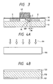
- the shape of the junction surface may be a constitution which is gradually remote from the gate, and is not particularly limited, but for avoiding unnecessary electrical field concentration, a smooth shape such as single flat plane as shown in Fig. 3, etc. is desirable.
- Such structure cannot be accomplished by using merely the MOS process known in the art, but as described later, must be positively formed such as by oblique implantation of ions from an angle of 10 and some degrees.
- the film thickness of the semiconductor layer which is the high impurity concentration region extremely thin as some 1000 ⁇ .
- the semiconductor region is a thin film of thin film SOI structure
- the region with the strongest electrical field within the device is not along the junction interface between the drain and the channel, but at the position determined by junction of the drain and the channel on the gate insulating film side, namely in the vicinity along the vertical line from the junction position to a position SEP in Fig. 3 of the subbing insulating substrate.
- the drain dielectric strength during OFF of the MOS type field effect transistor which was about 6 to 8 volt in the prior art can be improved to about 20 volt which had been unconceivable up to date.
- an insulating substrate itself of sapphire, alumina, glass, resin, etc., or alternatively, the insulating region formed in the semiconductor substrate or an insulating layer of silicon oxide, silicon nitride, etc. provided on a semiconductor substrate or an electroconductive substrate may be employed, and further an insulating layer of silicon oxide, silicon nitride, etc. as the protective layer provided on the substrate having elements with various functions formed thereon may be applicable.
- silicon oxide, silicon nitride, silicon oxynitride and etc. are used as the second insulating layer region.
- the upper gate stagger type As the structures of the gate electrode and the source-drain electrode, the upper gate stagger type, the lower gate stagger type, the upper gate coplanar type, the lower gate coplanar type, etc. may be employed.
- single crystalline layer and, non-single crystalline layer such as polycrystalline layer, microcrystalline layer comprising silicon as the matrix may be employed, but among them, single crystalline layer or polycrystalline layer having high carrier mobility is preferred.
- Fig. 3 is a schematic sectional view showing FET of SOI structure according to an embodiment of the present invention.
- 10 is a sapphire substrate as the substrate having insulating surface, 20 a semiconductor layer comprising a single crystalline silicon with a layer thickness of 2000 ⁇ formed on the sapphire substrate 10, 30 a silicon oxide film with a layer thickness of 500 ⁇ as the insulating layer provided on the semiconductor layer 20, and 40 a gate electrode comprising a polycrystalline silicon arranged on the silicon oxide film.
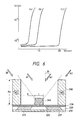
- Fig. 5 is a graph showing a result of comparison between the transistors respectively according to present invention and the prior art.
- the curve (a) in the Figure is the characteristics of the prior art type, the curve (b) the MOS type field effect transistor having an off-set structure, and the curve (c) the OFF characteristic of the MOS type field effect transistor having the structure of the present invention. It is shown that the present invention has not merely changed the prior art type to the off-set structure, but also attained a great effect through the action different therefrom.
- Fig. 5 shows the dielectric strength according to the embodiment shown in Fig. 1A, and (b) shows the dielectric strength according to the embodiment shown in Fig. 1B. While (c) shows the dielectric strength according to the present embodiment, and (a) is about 6 volt, and (b) is about 10 volt, a dielectric strength of about 21 volt was obtained in this embodiment.
- a drain interface S has an offset structure.
- a source interface is parallel to the drain interface and more closer to the gate electrode side as the closer to the underlayed interface.
- oxygen was injected onto the P-type single crystalline silicon substrate 100 with a plane direction of (100) with an impurity concentration of 1 x 10¹⁶/cm2 as shown by the arrowhead AA at an acceleration voltage of 150 kev, a total dose of 2.14 x 10¹⁸/cm2 and a substrate temperature of 600 °C. Then, annealing is applied in N2 gas at 1300 °C for 3 hours to form a P-type SIMOX substrate with a plane direction of (100) having the semiconductor layer 120 with a film thickness of 1000 ⁇ . 101 the lower semiconductor layer and 110 the first insulating layer (see Fig. 4B).
- a gate oxide film 130 with a thickness of 500 ⁇ by use of the thermal oxidation method was formed on the SOI substrate, and a polycrystalline film was formed by LPCVD thereon and P31 was ion injected into the polycrystalline silicon, followed by formation of a N-type gate polysilicon electrode with a thickness of 4000 ⁇ by patterning.
- the gate length was made 2 ⁇ m and the gate width 10 ⁇ m.
- P31 (phosphorus) was ion injected at an acceleration voltage of 60 kev from the direction in parallel to the source-drain direction (the direction in which current flows) and with an implantation angle of 43° ( ⁇ 1 in Fig. 4C), and subsequently a PSG film 150 was deposited to 6000 ⁇ as the interlayer insulating film, followed by application of the heat treatment at 900 °C for 15 minutes for activation of P31 (phosphorus).
- the implantation angle ⁇ 1 refers to an angle formed with the normal line direction of the gate insulating film 140 as shown in Fig. 4C.
- Formation of the source-drain region by oblique implantation of ions as described above has been practiced in bulk silicon process. Its object is channeling prevention or formation of off-set structure.
- oblique implantation of ions of the prior art has been applied on a device with a spread semiconductor without presence of a subbing insulating film.
- the present invention to cope with the problem inherent in the thin film SOI type field effect transistor with the high impurity concentration region reaching the subbing insulating film, has improved the drain dielectric strength during OFF through the action different from the prior art by utilizing the field distribution of the thin film SOI structure. In the following, description is made as compared with the prior art.
- the profile of impurities a structure as shown in Fig. 4D by oblique implantation of ions, (1) the junction interface between the drain and the channel susceptible to avalanche with the region with the strongest field is slipped, (2) and also the potential gradient became gentle corresponding to the slippage to lower the maximum field strength, whereby the drain dielectric strength during OFF was dramatically improved by about 15 volt from the A type of the prior art and about 11 volt from the B type. Also, as to ON characteristics, electrical field was relaxed in all the regions of the drain edge to improve the kinking phenomenon.
- Fig. 7 shows a sectional structure of the transistor according to the present embodiment.
- the source boundary also has the offset structure like the drain boundary, and is more remote from the gate electrode side in the direction toward underlayed interface.
- An SOI substrate with a film thickness of the silicon single crystal 220 (SOS) on the sapphire substrate 210 of 2000 ⁇ and an impurity concentration of 2 x 10¹⁶/cm3 was prepared, and a gate oxide film with a thickness of 800 ⁇ was formed by use of the thermal oxidation method.
- a polycrystalline silicon was deposited on the oxide film, P31 was ion injected and a N-type gate polysilicon electrode 240 with a thickness of 4000 ⁇ was formed by patterning.
- the gate length was made 2 ⁇ m, and the gate width 10 ⁇ m.
- a PSG film 250 was deposited to 6000 ⁇ , followed by application of heat treatment at 900 °C for 15 minutes for activation of phosphorus.
- a sectional structure with the junction interface S between the low impurity concentration region of channel 222 and the high impurity concentration region of drain 221 slanted about 30° relative to the subbing insulating film could be obtained.
- a drain electrode wiring 261, a source electrode wiring 22, a gate electrode wiring 263 and a protective layer 270 were formed.
- a thin film field effect transistor having the SOI structure shown in Fig. 7 was prepared.
- Fig. 8A shows a schematic illustration of the impurity profile in the sectional direction of the present embodiment
- Fig. 8B shows a reference, an impurity profile sectional view in the sectional direction when similar ion injection was effected in the case of low W1, W2 similarly as in conventional source-drain mask (namely Rx ⁇ tan ⁇ ⁇ X).
- W1, W2 are low, the junction interface has no slant, and the drain region will be spread to below the gate.
- a transistor with a junction interface between the drain and the channel produced by above described method is approximately 30 according to the above described production method. And, dielectric strength characteristic during OFF of the transistor thus measured. A result of the measurement is shown in Fig 9. Dielectric strength became a practical value of about 20 volt. Also, in ON characteristics, improvement of the kinking phenomenon was effected as compared with the prior art example in which reduction occurred similarly as in the mechanism of drain dielectric strength improvement during OFF in the whole region of the junction interface. Further, due to symmetrical structure, the lay-out is not restricted at all during circuit design, whereby its general purpose applicability could be expanded.
- the drain dielectric strengths V db of the respective samples during OFF were found to be 7 V, 8 V and 15 V.
- Fig. 10 shows the manner of such change in XA.
- the dielectric strength was found to be abruptly improved when L UP became 530 ⁇ or more.
- L UP /T SOI 0.35 or more the characteristics can be further improved.
- the off-set structure can be easily prepared, and during ON, there are the effects of reducing hot carriers, and improving the kinking phenomenon.
- Figs. 11A to 11D are schematic sectional views showing the preparation method of a semiconductor device according to an embodiment of the present invention.
- the structural members with the same constitution as those shown in the prior art example in Fig. 2 are attached with the same symbols.
- the present embodiment is most characterized in that an interface between the channel region and the low inpurity concentration drain region, and an interface between the low inpurity concentration drain region, and the high impurity drain region are both inclined.
- a semiconductor layer 302 of 700 ⁇ was formed on a thick insulating substrate 301 and then a gate insulating film 303 of 300 ⁇ was formed.
- phosphorus is diffused to effect etching of the polycrystalline silicon film by use of the photolithographic technique, to form a gate electrode 304.
- 5 x 10¹² of phosphorus (atoms/cm2) as in Fig. 4C are implanted as the impurity obliquely into the semiconductor layer by use of ion implantation, followed by annealing, to form a low concentration source 306 and a low concentration drain 307.
- a NSG film 308 is deposited to 3000 ⁇ , anisotropic etching effected by RIE to have the NSG film 308 remain only at the side wall of the polycrystalline film gate electrode 304, and then 1 x 10¹⁵ (atoms/cm2) of phosphorus are implanted obliquely into the semiconductor layer 302 by use of ion implantation to deposite a PSG film 311, followed by annealing, to form a source 309 and a drain 310.
- the PSG film 11 and the oxide film (insulating film) 303 are provided with openings 312 and 313, and electrodes 314 and 315 are formed to form the SOI type transistor of the present embodiment having trapezoidal sectional area.
- Fig. 12 is another embodiment of the preparation method of the SOI transistor of the present invention.
- a polycrystalline silicon film 304 doped with phosphorus and a source 306 and a drain 307 of low concentrations oxidation is carried out to form an oxide film.
- phosphorus is injected as the impurity into the source 309 and the drain 310 to form a PSG film 311, followed by annealing.
- the SOI type transistor of the present embodiment is formed.
- Figs. 13A to 13F are sectional views showing still another embodiment of the preparation steps of the semiconductor device of the present invention.
- a semiconductor layer 402 having a plane direction of (100) of 700 ⁇ is formed on the subbing insulating substrate 401, and then a gate insulating film 403 of 300 ⁇ is formed thereon.
- a polycrystalline silicon gate electrode 404 is deposited, and phosphorus is diffused to etch the polycrystalline silicon 4 by use of the photolithographic technique, followed by oxidation to form an oxide film 405 which is thicker than the insulating film 403 on the polycrystalline silicon gate electrode 404.
- KOH isopropil alcohol
- water e.g. (111) surface
- a polycrystalline silicon film is deposited, and the polycrystalline silicon film on the polycrystalline silicon gate electrode 404 is removed by etching by use of photolithographic technique, and then 5 x 10¹⁵ (atoms/cm2) of phosphorus are injected as the impurity by use of ion implantation to form polysilicon film 413, followed further by deposition of a PSG film 406.
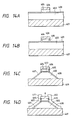
- Figs. 14A to 14D are still another embodiment showing the preparation steps according to the preparation method of the semiconductor device of the present invention.
- Fig. 14A after formation of the semiconductor layer 402 and the gate insulating film 403 on the insulating substrate 401 according to the same method as shown in Fig. 13A, deposition of the polysilicon film 404, phosphorus diffusion and deposition of the PSG film 406 are performed, and the PSG film 406 and the polycrystalline silicon film 404 are etched.
- oxidation is carried out, whereby an oxide film 405 grows at a side of the polycrystalline silicon film 404.
- the semiconductor layer 402 is anisotropically etched, 1 x 10¹⁵ (atoms/cm2) of phosphorus are injected as the impurity by use of ion implantation, followed further by heat treatment, to form a source 407 and a drain 408, so that inclined source-channel junction and inclined drain-channel junction are formed.
- electrodes 411 and 412 are formed as shown in Fig. 14D, to form the semiconductor device of the present embodiment.
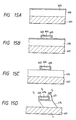
- Figs. 15A to 15F are diagrams of the steps showing still another embodiment of the preparation method of the semiconductor device of the present invention.
- the semiconductor 41 is anisotropically etched by reactive ion etching (R.I.E.) with the oxide film 415 as the resist mask using CCl2 F2, N2 and O2.
- a polycrystalline film 414 containing 2 x 10²⁰ of phosphorus (atoms/cm3) to 5000 ⁇ the polycrystalline silicon film 414 containing phosphorus on the oxide film 405 is removed by use of photolithographic technique, and then a PSG film 406 is deposited.
- electrodes 411 and 412 are formed to give the semiconductor device of the present embodiment.
- the angle formed between the subbing insulating substrate 1 and the drain layer 408 can be made slanted.
- transistor is applicable to electronic circuit device such as a three dimensioned integrated circuit, a contact type image sensor, a liquid crystal display device, and similar devices, to improve significantly the performance of them. Further, such electronic circuit device can be mounted within information processing apparatuses, such as a copier, a facsimile machine, an image reader, a word processer, a liquid crystal television set.
- information processing apparatuses such as a copier, a facsimile machine, an image reader, a word processer, a liquid crystal television set.
- Fig. 16A shows a circuit diagram of a contact type image sensor.
- the thin film transistor according to the present invention is formed as switch means for signal reading integrally together with a photoelectric conversion element on a common substrate.
- Fig. 16A a simple example comprising 4 segments x 2 blocks is shown for the purpose of easy understanding.
- Respective photo-receiving elements S1 - S8 are connected per a block commonly through block selection TFT switches SW1, SW2 to a reference voltage source VC. Another electrodes of respective photoreceiving elements S1 - S8 connected to segment selection TFT switches TSW1 to TSW8.
- Respective Gates of TFT switches TSW1 - TSW8 are connected commonly interconnected among corresponding segments in each block to constitute gate common lines, and scanned by shift-register SR.
- Respective sources are commonly interconnected and outputted via common output line V out .
- Such image sensor IS constitutes an information processing apparatus, together with a light source LS for illuminating an original, conveying roller TR, i.e., a maintaining means, for maintaining an original P at a reading position, and controlling means CONT for controlling the light source LS, the roller TR, and the image sensor IS (Fig. 16C).
- Fig 16B shows a circuit diagram of the liquid crystal display device.
- the thin film transistor of the present invention is for use in switches DSW1 - DSW4 driving liquid crystal cells LC1 - LC4 constituting respective pixels. Gates and sources thereof are connected in a matrix configuration, and driven by a vertical line selection shift register USR and a horizontal line selection shift register HSR.
- Such liquid display device is connected to the information processing apparatus as shown in Fig. 16C.
- the control means an output signal read by the sensor is supplied to the liquid crystal device to display an image.
- a monitor of the original reading can be achieved.
Landscapes
- Thin Film Transistor (AREA)
- Liquid Crystal (AREA)
- Solid State Image Pick-Up Elements (AREA)
Applications Claiming Priority (6)
| Application Number | Priority Date | Filing Date | Title |
|---|---|---|---|
| JP19826389 | 1989-07-31 | ||
| JP198263/89 | 1989-07-31 | ||
| JP217543/89 | 1989-08-25 | ||
| JP217542/89 | 1989-08-25 | ||
| JP21754389 | 1989-08-25 | ||
| JP21754289 | 1989-08-25 |
Publications (3)
| Publication Number | Publication Date |
|---|---|
| EP0412701A2 true EP0412701A2 (de) | 1991-02-13 |
| EP0412701A3 EP0412701A3 (de) | 1991-04-03 |
| EP0412701B1 EP0412701B1 (de) | 1996-09-25 |
Family
ID=27327477
Family Applications (1)
| Application Number | Title | Priority Date | Filing Date |
|---|---|---|---|
| EP90308353A Expired - Lifetime EP0412701B1 (de) | 1989-07-31 | 1990-07-30 | Dünnschicht-Transistor und seine Herstellung |
Country Status (4)
| Country | Link |
|---|---|
| US (1) | US5410172A (de) |
| EP (1) | EP0412701B1 (de) |
| JP (1) | JP2941908B2 (de) |
| DE (1) | DE69028669T2 (de) |
Cited By (5)
| Publication number | Priority date | Publication date | Assignee | Title |
|---|---|---|---|---|
| FR2709378A1 (fr) * | 1993-01-29 | 1995-03-03 | Mitsubishi Electric Corp | Transistor à effet de champ et procédé pour la fabrication d'un tel transistor. |
| US6013928A (en) * | 1991-08-23 | 2000-01-11 | Semiconductor Energy Laboratory Co., Ltd. | Semiconductor device having interlayer insulating film and method for forming the same |
| US6236064B1 (en) * | 1991-03-15 | 2001-05-22 | Semiconductor Energy Laboratory Co., Ltd. | Electro-optical device |
| US6713783B1 (en) | 1991-03-15 | 2004-03-30 | Semiconductor Energy Laboratory Co., Ltd. | Compensating electro-optical device including thin film transistors |
| US7855106B2 (en) | 1991-08-26 | 2010-12-21 | Semiconductor Energy Laboratory Co., Ltd. | Semiconductor device and method for forming the same |
Families Citing this family (26)
| Publication number | Priority date | Publication date | Assignee | Title |
|---|---|---|---|---|
| JP3437863B2 (ja) * | 1993-01-18 | 2003-08-18 | 株式会社半導体エネルギー研究所 | Mis型半導体装置の作製方法 |
| JP2838318B2 (ja) * | 1990-11-30 | 1998-12-16 | 株式会社半導体エネルギー研究所 | 感光装置及びその作製方法 |
| EP0499979A3 (en) | 1991-02-16 | 1993-06-09 | Semiconductor Energy Laboratory Co., Ltd. | Electro-optical device |
| US5719065A (en) | 1993-10-01 | 1998-02-17 | Semiconductor Energy Laboratory Co., Ltd. | Method for manufacturing semiconductor device with removable spacers |
| JPH07335904A (ja) * | 1994-06-14 | 1995-12-22 | Semiconductor Energy Lab Co Ltd | 薄膜半導体集積回路 |
| JPH07199150A (ja) * | 1993-12-28 | 1995-08-04 | Canon Inc | 液晶表示装置 |
| KR100205442B1 (ko) * | 1995-12-26 | 1999-07-01 | 구본준 | 박막트랜지스터 및 그의 제조방법 |
| KR0177785B1 (ko) * | 1996-02-03 | 1999-03-20 | 김광호 | 오프셋 구조를 가지는 트랜지스터 및 그 제조방법 |
| US5920085A (en) * | 1996-02-03 | 1999-07-06 | Samsung Electronics Co., Ltd. | Multiple floating gate field effect transistors and methods of operating same |
| FR2750534B1 (fr) * | 1996-06-27 | 1998-08-28 | Commissariat Energie Atomique | Transistor et procede de realisation d'un transistor a contacts et a isolation de champ auto-alignes |
| JP4318768B2 (ja) * | 1997-07-23 | 2009-08-26 | 株式会社半導体エネルギー研究所 | 半導体装置の作製方法 |
| JP3701832B2 (ja) * | 2000-02-04 | 2005-10-05 | インターナショナル・ビジネス・マシーンズ・コーポレーション | 薄膜トランジスタ、液晶表示パネル、および薄膜トランジスタの製造方法 |
| JP2002185011A (ja) * | 2000-12-19 | 2002-06-28 | Seiko Epson Corp | 半導体装置 |
| KR100366923B1 (ko) * | 2001-02-19 | 2003-01-06 | 삼성전자 주식회사 | 에스오아이 기판 및 이의 제조방법 |
| US6774486B2 (en) * | 2001-10-10 | 2004-08-10 | Micron Technology, Inc. | Circuit boards containing vias and methods for producing same |
| JP4278944B2 (ja) * | 2002-09-24 | 2009-06-17 | 東芝松下ディスプレイテクノロジー株式会社 | 光センサ素子、これを用いた平面表示装置 |
| JP2004219261A (ja) * | 2003-01-15 | 2004-08-05 | Fuji Photo Film Co Ltd | 薄膜の解析方法 |
| EP1588404A2 (de) * | 2003-01-17 | 2005-10-26 | General Electric Company | Waferhandhabungsvorrichtung |
| US20070015344A1 (en) * | 2003-06-26 | 2007-01-18 | Rj Mears, Llc | Method for Making a Semiconductor Device Including a Strained Superlattice Between at Least One Pair of Spaced Apart Stress Regions |
| US7531828B2 (en) * | 2003-06-26 | 2009-05-12 | Mears Technologies, Inc. | Semiconductor device including a strained superlattice between at least one pair of spaced apart stress regions |
| US20050195627A1 (en) * | 2003-11-18 | 2005-09-08 | Hutchens Chriswell G. | High-temperature memory systems |
| JP2006100721A (ja) * | 2004-09-30 | 2006-04-13 | Kobe Steel Ltd | 半導体素子及びその製造方法 |
| US7572706B2 (en) * | 2007-02-28 | 2009-08-11 | Freescale Semiconductor, Inc. | Source/drain stressor and method therefor |
| JP2016111105A (ja) * | 2014-12-03 | 2016-06-20 | 株式会社Joled | 薄膜トランジスタ及びその製造方法、並びに、表示装置 |
| CN109888021A (zh) * | 2019-02-27 | 2019-06-14 | 京东方科技集团股份有限公司 | 一种薄膜晶体管及其制备方法、阵列基板、显示装置 |
| KR20250035655A (ko) * | 2023-09-05 | 2025-03-13 | 삼성디스플레이 주식회사 | 표시 장치 및 그의 제조 방법 |
Family Cites Families (8)
| Publication number | Priority date | Publication date | Assignee | Title |
|---|---|---|---|---|
| EP0002107A3 (de) * | 1977-11-17 | 1979-09-05 | Rca Corporation | Verfahren zur Herstellung einer planaren Halbleiteranordnung |
| DE2948120C2 (de) * | 1978-11-29 | 1983-06-23 | Nippon Electric Co., Ltd., Tokyo | Isolierschicht-Feldeffekttransistor mit einer inselförmigen Halbleiterschicht auf einem isolierenden Substrat und Verfahren zur Herstellung eines derartigen Isolierschicht-Feldeffekttransistors |
| JPS5852881A (ja) * | 1981-09-25 | 1983-03-29 | Oki Electric Ind Co Ltd | 半導体素子の製造方法 |
| US4394182A (en) * | 1981-10-14 | 1983-07-19 | Rockwell International Corporation | Microelectronic shadow masking process for reducing punchthrough |
| EP0197531B1 (de) * | 1985-04-08 | 1993-07-28 | Hitachi, Ltd. | Dünnfilmtransistor auf isolierendem Substrat |
| JP2505736B2 (ja) * | 1985-06-18 | 1996-06-12 | キヤノン株式会社 | 半導体装置の製造方法 |
| FR2592224B1 (fr) * | 1985-12-20 | 1988-10-07 | Thomson Csf | Transistor a effet de champ, et circuit integre logique comportant un tel transistor |
| US4778258A (en) * | 1987-10-05 | 1988-10-18 | General Electric Company | Protective tab structure for use in the fabrication of matrix addressed thin film transistor liquid crystal displays |
-
1990
- 1990-07-30 DE DE69028669T patent/DE69028669T2/de not_active Expired - Fee Related
- 1990-07-30 EP EP90308353A patent/EP0412701B1/de not_active Expired - Lifetime
- 1990-07-30 JP JP20276190A patent/JP2941908B2/ja not_active Expired - Fee Related
-
1992
- 1992-12-23 US US07/996,887 patent/US5410172A/en not_active Expired - Fee Related
Cited By (5)
| Publication number | Priority date | Publication date | Assignee | Title |
|---|---|---|---|---|
| US6236064B1 (en) * | 1991-03-15 | 2001-05-22 | Semiconductor Energy Laboratory Co., Ltd. | Electro-optical device |
| US6713783B1 (en) | 1991-03-15 | 2004-03-30 | Semiconductor Energy Laboratory Co., Ltd. | Compensating electro-optical device including thin film transistors |
| US6013928A (en) * | 1991-08-23 | 2000-01-11 | Semiconductor Energy Laboratory Co., Ltd. | Semiconductor device having interlayer insulating film and method for forming the same |
| US7855106B2 (en) | 1991-08-26 | 2010-12-21 | Semiconductor Energy Laboratory Co., Ltd. | Semiconductor device and method for forming the same |
| FR2709378A1 (fr) * | 1993-01-29 | 1995-03-03 | Mitsubishi Electric Corp | Transistor à effet de champ et procédé pour la fabrication d'un tel transistor. |
Also Published As
| Publication number | Publication date |
|---|---|
| US5410172A (en) | 1995-04-25 |
| EP0412701B1 (de) | 1996-09-25 |
| DE69028669T2 (de) | 1997-02-20 |
| EP0412701A3 (de) | 1991-04-03 |
| DE69028669D1 (de) | 1996-10-31 |
| JPH03155676A (ja) | 1991-07-03 |
| JP2941908B2 (ja) | 1999-08-30 |
Similar Documents
| Publication | Publication Date | Title |
|---|---|---|
| EP0412701A2 (de) | Dünnschicht-Transistor und seine Herstellung | |
| US5504359A (en) | Vertical FET device with low gate to source overlap capacitance | |
| EP0494628B1 (de) | Verfahren zur Herstellung eines Mehrfachgate-Dünnfilmtransistors | |
| US6559478B1 (en) | Semiconductor integrated circuit and method of fabricating same | |
| US6759710B2 (en) | Self-aligned double-gate MOSFET by selective epitaxy and silicon wafer bonding techniques | |
| JP3361922B2 (ja) | 半導体装置 | |
| US4686758A (en) | Three-dimensional CMOS using selective epitaxial growth | |
| US5488005A (en) | Process for manufacturing an offset gate structure thin film transistor | |
| US5073519A (en) | Method of fabricating a vertical FET device with low gate to drain overlap capacitance | |
| US5840602A (en) | Methods of forming nonmonocrystalline silicon-on-insulator thin-film transistors | |
| EP0521702B1 (de) | Halbleiteranordnung mit verschmolzenen bipolaren und MOS-Transistoren und Herstellungsverfahren | |
| EP0782182A2 (de) | MOS-Transistor und Verfahren zu seiner Herstellung | |
| US5723879A (en) | Thin film transistor with vertical channel adjacent sidewall of gate electrode and method of making | |
| JPH06349853A (ja) | Mosトランジスタおよびその製造方法 | |
| KR970009054B1 (ko) | 평면구조 모스 트랜지스터 및 그 제조방법 | |
| KR100328126B1 (ko) | 트렌치게이트구조를갖는다결정실리콘박막트랜지스터의제조방법 | |
| US5646055A (en) | Method for making bipolar transistor | |
| US8008718B2 (en) | Semiconductor device and production method thereof | |
| JP3391176B2 (ja) | 薄膜トランジスタの製造方法 | |
| JPH0350771A (ja) | 半導体装置 | |
| JPH04364074A (ja) | 絶縁ゲート電界効果トランジスタ | |
| JP2504630B2 (ja) | アクティブマトリックス基板 | |
| KR100197656B1 (ko) | 반도체 에스.오.아이.소자의 제조방법 | |
| WO1993017458A1 (fr) | Dispositif semiconducteur a substrat de silicium et procede de realisation | |
| JPH07273340A (ja) | Soi型トランジスタ |
Legal Events
| Date | Code | Title | Description |
|---|---|---|---|
| PUAI | Public reference made under article 153(3) epc to a published international application that has entered the european phase |
Free format text: ORIGINAL CODE: 0009012 |
|
| PUAL | Search report despatched |
Free format text: ORIGINAL CODE: 0009013 |
|
| AK | Designated contracting states |
Kind code of ref document: A2 Designated state(s): DE FR GB NL |
|
| 17P | Request for examination filed |
Effective date: 19901231 |
|
| AK | Designated contracting states |
Kind code of ref document: A3 Designated state(s): DE FR GB NL |
|
| 17Q | First examination report despatched |
Effective date: 19940209 |
|
| GRAH | Despatch of communication of intention to grant a patent |
Free format text: ORIGINAL CODE: EPIDOS IGRA |
|
| GRAH | Despatch of communication of intention to grant a patent |
Free format text: ORIGINAL CODE: EPIDOS IGRA |
|
| GRAA | (expected) grant |
Free format text: ORIGINAL CODE: 0009210 |
|
| AK | Designated contracting states |
Kind code of ref document: B1 Designated state(s): DE FR GB NL |
|
| REF | Corresponds to: |
Ref document number: 69028669 Country of ref document: DE Date of ref document: 19961031 |
|
| ET | Fr: translation filed | ||
| PLBE | No opposition filed within time limit |
Free format text: ORIGINAL CODE: 0009261 |
|
| STAA | Information on the status of an ep patent application or granted ep patent |
Free format text: STATUS: NO OPPOSITION FILED WITHIN TIME LIMIT |
|
| 26N | No opposition filed | ||
| REG | Reference to a national code |
Ref country code: GB Ref legal event code: IF02 |
|
| PGFP | Annual fee paid to national office [announced via postgrant information from national office to epo] |
Ref country code: NL Payment date: 20050715 Year of fee payment: 16 |
|
| PGFP | Annual fee paid to national office [announced via postgrant information from national office to epo] |
Ref country code: GB Payment date: 20050718 Year of fee payment: 16 |
|
| PGFP | Annual fee paid to national office [announced via postgrant information from national office to epo] |
Ref country code: FR Payment date: 20050719 Year of fee payment: 16 |
|
| PGFP | Annual fee paid to national office [announced via postgrant information from national office to epo] |
Ref country code: DE Payment date: 20050912 Year of fee payment: 16 |
|
| PG25 | Lapsed in a contracting state [announced via postgrant information from national office to epo] |
Ref country code: GB Free format text: LAPSE BECAUSE OF NON-PAYMENT OF DUE FEES Effective date: 20060730 |
|
| PG25 | Lapsed in a contracting state [announced via postgrant information from national office to epo] |
Ref country code: DE Free format text: LAPSE BECAUSE OF NON-PAYMENT OF DUE FEES Effective date: 20070201 Ref country code: NL Free format text: LAPSE BECAUSE OF NON-PAYMENT OF DUE FEES Effective date: 20070201 |
|
| GBPC | Gb: european patent ceased through non-payment of renewal fee |
Effective date: 20060730 |
|
| NLV4 | Nl: lapsed or anulled due to non-payment of the annual fee |
Effective date: 20070201 |
|
| REG | Reference to a national code |
Ref country code: FR Ref legal event code: ST Effective date: 20070330 |
|
| PG25 | Lapsed in a contracting state [announced via postgrant information from national office to epo] |
Ref country code: FR Free format text: LAPSE BECAUSE OF NON-PAYMENT OF DUE FEES Effective date: 20060731 |