EP0412850A2 - Substrat für Aufzeichnungsmedium, Aufzeichnungsmedium, Verfahren zur Herstellung dergleichen, Aufzeichnungs- und Wiedergabeeinrichtung und Verfahren zur Aufzeichnung, Wiedergabe und Löschen mit Gebrauch von einem solchen Aufzeichnungsmedium - Google Patents
Substrat für Aufzeichnungsmedium, Aufzeichnungsmedium, Verfahren zur Herstellung dergleichen, Aufzeichnungs- und Wiedergabeeinrichtung und Verfahren zur Aufzeichnung, Wiedergabe und Löschen mit Gebrauch von einem solchen Aufzeichnungsmedium Download PDFInfo
- Publication number
- EP0412850A2 EP0412850A2 EP90308858A EP90308858A EP0412850A2 EP 0412850 A2 EP0412850 A2 EP 0412850A2 EP 90308858 A EP90308858 A EP 90308858A EP 90308858 A EP90308858 A EP 90308858A EP 0412850 A2 EP0412850 A2 EP 0412850A2
- Authority
- EP
- European Patent Office
- Prior art keywords
- recording
- recording medium
- substrate
- track
- electrode
- Prior art date
- Legal status (The legal status is an assumption and is not a legal conclusion. Google has not performed a legal analysis and makes no representation as to the accuracy of the status listed.)
- Granted
Links
- 239000000758 substrate Substances 0.000 title claims abstract description 78
- 238000000034 method Methods 0.000 title claims description 72
- 239000000523 sample Substances 0.000 claims abstract description 98
- 229910052751 metal Inorganic materials 0.000 claims abstract description 27
- 239000002184 metal Substances 0.000 claims abstract description 27
- 238000010894 electron beam technology Methods 0.000 claims abstract description 16
- 239000011882 ultra-fine particle Substances 0.000 claims abstract description 12
- 238000000151 deposition Methods 0.000 claims abstract description 6
- 230000001678 irradiating effect Effects 0.000 claims abstract description 5
- 239000010410 layer Substances 0.000 claims description 56
- 239000000463 material Substances 0.000 claims description 22
- 239000004065 semiconductor Substances 0.000 claims description 10
- PCHJSUWPFVWCPO-UHFFFAOYSA-N gold Chemical compound [Au] PCHJSUWPFVWCPO-UHFFFAOYSA-N 0.000 claims description 9
- 229910052737 gold Inorganic materials 0.000 claims description 9
- 239000010931 gold Substances 0.000 claims description 9
- 239000002356 single layer Substances 0.000 claims description 8
- 230000003446 memory effect Effects 0.000 claims description 7
- 150000002894 organic compounds Chemical class 0.000 claims description 5
- XUIMIQQOPSSXEZ-UHFFFAOYSA-N Silicon Chemical compound [Si] XUIMIQQOPSSXEZ-UHFFFAOYSA-N 0.000 claims description 3
- 229910052710 silicon Inorganic materials 0.000 claims description 3
- 239000010703 silicon Substances 0.000 claims description 3
- 239000002245 particle Substances 0.000 claims description 2
- 239000010408 film Substances 0.000 description 30
- 239000004642 Polyimide Substances 0.000 description 8
- 230000015654 memory Effects 0.000 description 8
- 229920001721 polyimide Polymers 0.000 description 8
- XLYOFNOQVPJJNP-UHFFFAOYSA-N water Substances O XLYOFNOQVPJJNP-UHFFFAOYSA-N 0.000 description 8
- 238000004574 scanning tunneling microscopy Methods 0.000 description 7
- 238000007740 vapor deposition Methods 0.000 description 7
- 229910021417 amorphous silicon Inorganic materials 0.000 description 6
- 150000001875 compounds Chemical class 0.000 description 6
- 239000000975 dye Substances 0.000 description 6
- 239000000126 substance Substances 0.000 description 6
- 239000004952 Polyamide Substances 0.000 description 5
- 238000006073 displacement reaction Methods 0.000 description 5
- 230000007246 mechanism Effects 0.000 description 5
- 229920002647 polyamide Polymers 0.000 description 5
- 229910052709 silver Inorganic materials 0.000 description 5
- 239000004332 silver Substances 0.000 description 5
- 239000002253 acid Substances 0.000 description 4
- UHOVQNZJYSORNB-UHFFFAOYSA-N benzene Substances C1=CC=CC=C1 UHOVQNZJYSORNB-UHFFFAOYSA-N 0.000 description 4
- 230000015572 biosynthetic process Effects 0.000 description 4
- 229920001577 copolymer Polymers 0.000 description 4
- 238000010586 diagram Methods 0.000 description 4
- -1 etc. Substances 0.000 description 4
- 230000002209 hydrophobic effect Effects 0.000 description 4
- BASFCYQUMIYNBI-UHFFFAOYSA-N platinum Chemical compound [Pt] BASFCYQUMIYNBI-UHFFFAOYSA-N 0.000 description 4
- VZCYOOQTPOCHFL-UHFFFAOYSA-N trans-butenedioic acid Natural products OC(=O)C=CC(O)=O VZCYOOQTPOCHFL-UHFFFAOYSA-N 0.000 description 4
- 230000004304 visual acuity Effects 0.000 description 4
- RYGMFSIKBFXOCR-UHFFFAOYSA-N Copper Chemical compound [Cu] RYGMFSIKBFXOCR-UHFFFAOYSA-N 0.000 description 3
- REYJJPSVUYRZGE-UHFFFAOYSA-N Octadecylamine Chemical class CCCCCCCCCCCCCCCCCCN REYJJPSVUYRZGE-UHFFFAOYSA-N 0.000 description 3
- 239000005387 chalcogenide glass Substances 0.000 description 3
- 229910052802 copper Inorganic materials 0.000 description 3
- 239000010949 copper Substances 0.000 description 3
- 238000002474 experimental method Methods 0.000 description 3
- 238000010884 ion-beam technique Methods 0.000 description 3
- 230000003287 optical effect Effects 0.000 description 3
- 239000002904 solvent Substances 0.000 description 3
- 238000012360 testing method Methods 0.000 description 3
- 239000010409 thin film Substances 0.000 description 3
- IXHWGNYCZPISET-UHFFFAOYSA-N 2-[4-(dicyanomethylidene)-2,3,5,6-tetrafluorocyclohexa-2,5-dien-1-ylidene]propanedinitrile Chemical compound FC1=C(F)C(=C(C#N)C#N)C(F)=C(F)C1=C(C#N)C#N IXHWGNYCZPISET-UHFFFAOYSA-N 0.000 description 2
- JLTPSDHKZGWXTD-UHFFFAOYSA-N 2-[6-(dicyanomethylidene)naphthalen-2-ylidene]propanedinitrile Chemical compound N#CC(C#N)=C1C=CC2=CC(=C(C#N)C#N)C=CC2=C1 JLTPSDHKZGWXTD-UHFFFAOYSA-N 0.000 description 2
- NLZUEZXRPGMBCV-UHFFFAOYSA-N Butylhydroxytoluene Chemical compound CC1=CC(C(C)(C)C)=C(O)C(C(C)(C)C)=C1 NLZUEZXRPGMBCV-UHFFFAOYSA-N 0.000 description 2
- VYZAMTAEIAYCRO-UHFFFAOYSA-N Chromium Chemical compound [Cr] VYZAMTAEIAYCRO-UHFFFAOYSA-N 0.000 description 2
- VZCYOOQTPOCHFL-OWOJBTEDSA-N Fumaric acid Natural products OC(=O)\C=C\C(O)=O VZCYOOQTPOCHFL-OWOJBTEDSA-N 0.000 description 2
- OFOBLEOULBTSOW-UHFFFAOYSA-N Propanedioic acid Natural products OC(=O)CC(O)=O OFOBLEOULBTSOW-UHFFFAOYSA-N 0.000 description 2
- BQCADISMDOOEFD-UHFFFAOYSA-N Silver Chemical compound [Ag] BQCADISMDOOEFD-UHFFFAOYSA-N 0.000 description 2
- 229920002125 Sokalan® Polymers 0.000 description 2
- MWPLVEDNUUSJAV-UHFFFAOYSA-N anthracene Chemical compound C1=CC=CC2=CC3=CC=CC=C3C=C21 MWPLVEDNUUSJAV-UHFFFAOYSA-N 0.000 description 2
- CUFNKYGDVFVPHO-UHFFFAOYSA-N azulene Chemical compound C1=CC=CC2=CC=CC2=C1 CUFNKYGDVFVPHO-UHFFFAOYSA-N 0.000 description 2
- IOJUPLGTWVMSFF-UHFFFAOYSA-N benzothiazole Chemical group C1=CC=C2SC=NC2=C1 IOJUPLGTWVMSFF-UHFFFAOYSA-N 0.000 description 2
- 230000008859 change Effects 0.000 description 2
- 229910052804 chromium Inorganic materials 0.000 description 2
- 239000011651 chromium Substances 0.000 description 2
- 229910017052 cobalt Inorganic materials 0.000 description 2
- 239000010941 cobalt Substances 0.000 description 2
- GUTLYIVDDKVIGB-UHFFFAOYSA-N cobalt atom Chemical compound [Co] GUTLYIVDDKVIGB-UHFFFAOYSA-N 0.000 description 2
- 238000012937 correction Methods 0.000 description 2
- 238000001514 detection method Methods 0.000 description 2
- 230000000694 effects Effects 0.000 description 2
- 238000005530 etching Methods 0.000 description 2
- 230000008020 evaporation Effects 0.000 description 2
- 238000001704 evaporation Methods 0.000 description 2
- 239000001530 fumaric acid Substances 0.000 description 2
- 125000001165 hydrophobic group Chemical group 0.000 description 2
- 230000000977 initiatory effect Effects 0.000 description 2
- 239000011976 maleic acid Substances 0.000 description 2
- 238000005259 measurement Methods 0.000 description 2
- 125000001434 methanylylidene group Chemical group [H]C#[*] 0.000 description 2
- IEQIEDJGQAUEQZ-UHFFFAOYSA-N phthalocyanine Chemical compound N1C(N=C2C3=CC=CC=C3C(N=C3C4=CC=CC=C4C(=N4)N3)=N2)=C(C=CC=C2)C2=C1N=C1C2=CC=CC=C2C4=N1 IEQIEDJGQAUEQZ-UHFFFAOYSA-N 0.000 description 2
- 229910052697 platinum Inorganic materials 0.000 description 2
- 229920000642 polymer Polymers 0.000 description 2
- 238000002360 preparation method Methods 0.000 description 2
- BBEAQIROQSPTKN-UHFFFAOYSA-N pyrene Chemical compound C1=CC=C2C=CC3=CC=CC4=CC=C1C2=C43 BBEAQIROQSPTKN-UHFFFAOYSA-N 0.000 description 2
- NLDYACGHTUPAQU-UHFFFAOYSA-N tetracyanoethylene Chemical group N#CC(C#N)=C(C#N)C#N NLDYACGHTUPAQU-UHFFFAOYSA-N 0.000 description 2
- QGKMIGUHVLGJBR-UHFFFAOYSA-M (4z)-1-(3-methylbutyl)-4-[[1-(3-methylbutyl)quinolin-1-ium-4-yl]methylidene]quinoline;iodide Chemical compound [I-].C12=CC=CC=C2N(CCC(C)C)C=CC1=CC1=CC=[N+](CCC(C)C)C2=CC=CC=C12 QGKMIGUHVLGJBR-UHFFFAOYSA-M 0.000 description 1
- BCMCBBGGLRIHSE-UHFFFAOYSA-N 1,3-benzoxazole Chemical group C1=CC=C2OC=NC2=C1 BCMCBBGGLRIHSE-UHFFFAOYSA-N 0.000 description 1
- BZSVVCFHMVMYCR-UHFFFAOYSA-N 2-pyridin-2-ylpyridine;ruthenium Chemical class [Ru].N1=CC=CC=C1C1=CC=CC=N1.N1=CC=CC=C1C1=CC=CC=N1.N1=CC=CC=C1C1=CC=CC=N1 BZSVVCFHMVMYCR-UHFFFAOYSA-N 0.000 description 1
- 229920002126 Acrylic acid copolymer Polymers 0.000 description 1
- 229910002710 Au-Pd Inorganic materials 0.000 description 1
- 108010082845 Bacteriorhodopsins Proteins 0.000 description 1
- 102000018832 Cytochromes Human genes 0.000 description 1
- 108010052832 Cytochromes Proteins 0.000 description 1
- DFPAKSUCGFBDDF-UHFFFAOYSA-N Nicotinamide Chemical group NC(=O)C1=CC=CN=C1 DFPAKSUCGFBDDF-UHFFFAOYSA-N 0.000 description 1
- 229910018110 Se—Te Inorganic materials 0.000 description 1
- 230000001133 acceleration Effects 0.000 description 1
- 230000004913 activation Effects 0.000 description 1
- 229910045601 alloy Inorganic materials 0.000 description 1
- 239000000956 alloy Substances 0.000 description 1
- 229910052782 aluminium Inorganic materials 0.000 description 1
- XAGFODPZIPBFFR-UHFFFAOYSA-N aluminium Chemical compound [Al] XAGFODPZIPBFFR-UHFFFAOYSA-N 0.000 description 1
- 125000003277 amino group Chemical group 0.000 description 1
- SMWDFEZZVXVKRB-UHFFFAOYSA-N anhydrous quinoline Natural products N1=CC=CC2=CC=CC=C21 SMWDFEZZVXVKRB-UHFFFAOYSA-N 0.000 description 1
- 238000013459 approach Methods 0.000 description 1
- 125000003118 aryl group Chemical group 0.000 description 1
- 230000008901 benefit Effects 0.000 description 1
- 239000005385 borate glass Substances 0.000 description 1
- LLCSWKVOHICRDD-UHFFFAOYSA-N buta-1,3-diyne Chemical group C#CC#C LLCSWKVOHICRDD-UHFFFAOYSA-N 0.000 description 1
- 125000003178 carboxy group Chemical group [H]OC(*)=O 0.000 description 1
- 150000004770 chalcogenides Chemical class 0.000 description 1
- 239000004020 conductor Substances 0.000 description 1
- 238000012790 confirmation Methods 0.000 description 1
- 239000000470 constituent Substances 0.000 description 1
- 150000001923 cyclic compounds Chemical class 0.000 description 1
- 238000011161 development Methods 0.000 description 1
- 230000018109 developmental process Effects 0.000 description 1
- NAPSCFZYZVSQHF-UHFFFAOYSA-N dimantine Chemical compound CCCCCCCCCCCCCCCCCCN(C)C NAPSCFZYZVSQHF-UHFFFAOYSA-N 0.000 description 1
- 230000005684 electric field Effects 0.000 description 1
- 230000002708 enhancing effect Effects 0.000 description 1
- 125000004185 ester group Chemical group 0.000 description 1
- CEIPQQODRKXDSB-UHFFFAOYSA-N ethyl 3-(6-hydroxynaphthalen-2-yl)-1H-indazole-5-carboximidate dihydrochloride Chemical compound Cl.Cl.C1=C(O)C=CC2=CC(C3=NNC4=CC=C(C=C43)C(=N)OCC)=CC=C21 CEIPQQODRKXDSB-UHFFFAOYSA-N 0.000 description 1
- KTWOOEGAPBSYNW-UHFFFAOYSA-N ferrocene Chemical compound [Fe+2].C=1C=C[CH-]C=1.C=1C=C[CH-]C=1 KTWOOEGAPBSYNW-UHFFFAOYSA-N 0.000 description 1
- GVEPBJHOBDJJJI-UHFFFAOYSA-N fluoranthrene Natural products C1=CC(C2=CC=CC=C22)=C3C2=CC=CC3=C1 GVEPBJHOBDJJJI-UHFFFAOYSA-N 0.000 description 1
- PQTCMBYFWMFIGM-UHFFFAOYSA-N gold silver Chemical compound [Ag].[Au] PQTCMBYFWMFIGM-UHFFFAOYSA-N 0.000 description 1
- 238000010438 heat treatment Methods 0.000 description 1
- 150000002391 heterocyclic compounds Chemical class 0.000 description 1
- 125000000623 heterocyclic group Chemical group 0.000 description 1
- 150000002430 hydrocarbons Chemical group 0.000 description 1
- 125000002887 hydroxy group Chemical group [H]O* 0.000 description 1
- 125000005462 imide group Chemical group 0.000 description 1
- 239000012212 insulator Substances 0.000 description 1
- 230000003993 interaction Effects 0.000 description 1
- 150000002605 large molecules Chemical class 0.000 description 1
- 239000000696 magnetic material Substances 0.000 description 1
- 150000002739 metals Chemical class 0.000 description 1
- 238000012544 monitoring process Methods 0.000 description 1
- 239000000178 monomer Substances 0.000 description 1
- 229910052757 nitrogen Inorganic materials 0.000 description 1
- QJGQUHMNIGDVPM-UHFFFAOYSA-N nitrogen group Chemical group [N] QJGQUHMNIGDVPM-UHFFFAOYSA-N 0.000 description 1
- 239000000075 oxide glass Substances 0.000 description 1
- 230000000737 periodic effect Effects 0.000 description 1
- 125000001997 phenyl group Chemical group [H]C1=C([H])C([H])=C(*)C([H])=C1[H] 0.000 description 1
- PXXKQOPKNFECSZ-UHFFFAOYSA-N platinum rhodium Chemical compound [Rh].[Pt] PXXKQOPKNFECSZ-UHFFFAOYSA-N 0.000 description 1
- 229920005575 poly(amic acid) Polymers 0.000 description 1
- 239000004584 polyacrylic acid Substances 0.000 description 1
- 125000003367 polycyclic group Chemical group 0.000 description 1
- 229920000015 polydiacetylene Polymers 0.000 description 1
- 238000006116 polymerization reaction Methods 0.000 description 1
- 229920001184 polypeptide Polymers 0.000 description 1
- 230000002265 prevention Effects 0.000 description 1
- 102000004196 processed proteins & peptides Human genes 0.000 description 1
- 108090000765 processed proteins & peptides Proteins 0.000 description 1
- 125000002943 quinolinyl group Chemical group N1=C(C=CC2=CC=CC=C12)* 0.000 description 1
- 230000009467 reduction Effects 0.000 description 1
- 230000004044 response Effects 0.000 description 1
- 150000003839 salts Chemical class 0.000 description 1
- 229920006395 saturated elastomer Polymers 0.000 description 1
- 229930195734 saturated hydrocarbon Natural products 0.000 description 1
- 239000011877 solvent mixture Substances 0.000 description 1
- 238000004544 sputter deposition Methods 0.000 description 1
- YNHJECZULSZAQK-UHFFFAOYSA-N tetraphenylporphyrin Chemical compound C1=CC(C(=C2C=CC(N2)=C(C=2C=CC=CC=2)C=2C=CC(N=2)=C(C=2C=CC=CC=2)C2=CC=C3N2)C=2C=CC=CC=2)=NC1=C3C1=CC=CC=C1 YNHJECZULSZAQK-UHFFFAOYSA-N 0.000 description 1
- 238000012546 transfer Methods 0.000 description 1
- WFKWXMTUELFFGS-UHFFFAOYSA-N tungsten Chemical compound [W] WFKWXMTUELFFGS-UHFFFAOYSA-N 0.000 description 1
- 229910052721 tungsten Inorganic materials 0.000 description 1
- 239000010937 tungsten Substances 0.000 description 1
- 229930195735 unsaturated hydrocarbon Natural products 0.000 description 1
- 125000000391 vinyl group Chemical group [H]C([*])=C([H])[H] 0.000 description 1
- 229910052727 yttrium Inorganic materials 0.000 description 1
Images



Classifications
-
- G—PHYSICS
- G11—INFORMATION STORAGE
- G11B—INFORMATION STORAGE BASED ON RELATIVE MOVEMENT BETWEEN RECORD CARRIER AND TRANSDUCER
- G11B9/00—Recording or reproducing using a method not covered by one of the main groups G11B3/00 - G11B7/00; Record carriers therefor
- G11B9/12—Recording or reproducing using a method not covered by one of the main groups G11B3/00 - G11B7/00; Record carriers therefor using near-field interactions; Record carriers therefor
- G11B9/14—Recording or reproducing using a method not covered by one of the main groups G11B3/00 - G11B7/00; Record carriers therefor using near-field interactions; Record carriers therefor using microscopic probe means, i.e. recording or reproducing by means directly associated with the tip of a microscopic electrical probe as used in Scanning Tunneling Microscopy [STM] or Atomic Force Microscopy [AFM] for inducing physical or electrical perturbations in a recording medium; Record carriers or media specially adapted for such transducing of information
- G11B9/1463—Record carriers for recording or reproduction involving the use of microscopic probe means
- G11B9/1472—Record carriers for recording or reproduction involving the use of microscopic probe means characterised by the form
- G11B9/1481—Auxiliary features, e.g. reference or indexing surfaces
-
- G—PHYSICS
- G11—INFORMATION STORAGE
- G11B—INFORMATION STORAGE BASED ON RELATIVE MOVEMENT BETWEEN RECORD CARRIER AND TRANSDUCER
- G11B9/00—Recording or reproducing using a method not covered by one of the main groups G11B3/00 - G11B7/00; Record carriers therefor
- G11B9/12—Recording or reproducing using a method not covered by one of the main groups G11B3/00 - G11B7/00; Record carriers therefor using near-field interactions; Record carriers therefor
- G11B9/14—Recording or reproducing using a method not covered by one of the main groups G11B3/00 - G11B7/00; Record carriers therefor using near-field interactions; Record carriers therefor using microscopic probe means, i.e. recording or reproducing by means directly associated with the tip of a microscopic electrical probe as used in Scanning Tunneling Microscopy [STM] or Atomic Force Microscopy [AFM] for inducing physical or electrical perturbations in a recording medium; Record carriers or media specially adapted for such transducing of information
-
- G—PHYSICS
- G11—INFORMATION STORAGE
- G11B—INFORMATION STORAGE BASED ON RELATIVE MOVEMENT BETWEEN RECORD CARRIER AND TRANSDUCER
- G11B9/00—Recording or reproducing using a method not covered by one of the main groups G11B3/00 - G11B7/00; Record carriers therefor
- G11B9/12—Recording or reproducing using a method not covered by one of the main groups G11B3/00 - G11B7/00; Record carriers therefor using near-field interactions; Record carriers therefor
- G11B9/14—Recording or reproducing using a method not covered by one of the main groups G11B3/00 - G11B7/00; Record carriers therefor using near-field interactions; Record carriers therefor using microscopic probe means, i.e. recording or reproducing by means directly associated with the tip of a microscopic electrical probe as used in Scanning Tunneling Microscopy [STM] or Atomic Force Microscopy [AFM] for inducing physical or electrical perturbations in a recording medium; Record carriers or media specially adapted for such transducing of information
- G11B9/1463—Record carriers for recording or reproduction involving the use of microscopic probe means
-
- B—PERFORMING OPERATIONS; TRANSPORTING
- B82—NANOTECHNOLOGY
- B82Y—SPECIFIC USES OR APPLICATIONS OF NANOSTRUCTURES; MEASUREMENT OR ANALYSIS OF NANOSTRUCTURES; MANUFACTURE OR TREATMENT OF NANOSTRUCTURES
- B82Y10/00—Nanotechnology for information processing, storage or transmission, e.g. quantum computing or single electron logic
-
- Y—GENERAL TAGGING OF NEW TECHNOLOGICAL DEVELOPMENTS; GENERAL TAGGING OF CROSS-SECTIONAL TECHNOLOGIES SPANNING OVER SEVERAL SECTIONS OF THE IPC; TECHNICAL SUBJECTS COVERED BY FORMER USPC CROSS-REFERENCE ART COLLECTIONS [XRACs] AND DIGESTS
- Y10—TECHNICAL SUBJECTS COVERED BY FORMER USPC
- Y10S—TECHNICAL SUBJECTS COVERED BY FORMER USPC CROSS-REFERENCE ART COLLECTIONS [XRACs] AND DIGESTS
- Y10S977/00—Nanotechnology
- Y10S977/902—Specified use of nanostructure
- Y10S977/932—Specified use of nanostructure for electronic or optoelectronic application
- Y10S977/943—Information storage or retrieval using nanostructure
- Y10S977/947—Information storage or retrieval using nanostructure with scanning probe instrument
Definitions
- This invention relates to a recording medium and a substrate for recording medium to be used for a recording and reproducing device which performs recording and reproduction by use of a scanning probe wherein reproducibility of recording and reproduction of information is improved, and also to a method for preparation thereof.
- the present invention relates to a recording, reproducing and erasing method and a recording and reproducing device which performs recording and reproduction with good reproducibility by use of such a recording medium.
- semiconductor memories or magnetic memories employing magnetic material or semiconductor as the base material have been predominant, but with the advancement of laser technique, inexpensive and high density recording media with optical memory by use of an organic thin film such as organic dye, photopolymer, etc. are now emerging in the field of art.
- STM scanning type tunnel microscope
- STM is based on the phenomenon that tunnel current flows when a probe and an electroconductive substance are made to approach to a distance of about 1 nm with a voltage applied therebetween. This current is very sensitive to the distance change between them, and by scanning the probe so that the tunnel current may be maintained to be constant, the surface structure of the real space can be drawn and at the same time a variety of information about the total electron cloud of surface atoms can be read.
- resolving power in the interplanar direction is about 1 ⁇ . Therefore, by applying the principle of STM, it is possible to perform high density recording and reproduction sufficiently in the order of an interatomic distance (several ⁇ ).
- a recording and reproducing method in this case there have been proposed a method in which recording is performed by changing the surface state of an appropriate recording layer by use of a particle ray (electron beam, ion beam) or a high energy electromagnetic wave such as X-ray or an energy ray such as visible light or UV-ray, etc., and reproduction is effected by STM, and a method in which a material having a memory effect for switching characteristics of voltage and current, for example, a ⁇ -electron type organic compound or a chalcogenide thin film, is used as the recording layer, and recording and reproduction are performed by use of STM, etc. (Japanese Patent Laid-oOpen No. 63-204531, No. 63-161552, No. 63-161553).
- AFM intramolecular force microscope
- an object of the present invention is to provide a recording medium and a substrate therefor which can practice recording and reproduction of a large amount of information easily and with good reproducibility in a high density recording and reproducing method by use of a scanning probe, and a method for preparing the same.
- the present invention provides a substrate for recording medium having a track with a width in the range of from 40 ⁇ to 400 ⁇ .
- the present invention also provides a method for preparing a substrate for recording medium, which comprises the step of irradiating an electron beam on a substrate following a certain pattern and the step of forming a track comprising ultra-fine particles of a metal by vapor depositing the metal onto the substrate.
- the present invention also provides a method for preparing an electrode substrate, which comprises the step of irradiating an electron beam on a substrate following a certain pattern, the step of forming a track comprising ultra-fine particles of a metal by vapor depositing the metal onto the substrate and the step of providing a metal layer on the substrate.
- the present invention also provides a recording medium having a track with a width in the range of from 40 ⁇ to 400 ⁇ on a recording surface.
- the present invention also provides a method for preparing a recording medium, which comprises the step of irradiating an electron beam following a certain pattern on a substrate, the step of forming a track comprising ultra-fine particles of a metal by vapor depositing the metal onto the substrate, the step of providing a metal layer on the substrate and the step of providing a recording layer on the metal layer.
- the present invention also provides a recording method which comprises accessing a probe to a recording medium having the track on a recording surface and performing recording through the probe electrode on the track.
- the present invention also provides a recording and reproducing method, which comprises performing recording on a track by accessing a probe to a recording medium having the track on a recording surface and applying a pulse voltage between a substrate electrode and a probe electrode, and reproducing the recorded information by applying a bias voltage between the substrate electrode and the probe electrode.
- the present invention also provides a recording, reproducing and erasing method, which comprises performing recording on a track by accessing a probe to a recording medium having the track on a recording surface and applying a pulse voltage between a substrate electrode and a probe electrode, reproducing the recorded information by applying a bias voltage between the substrate electrode and the probe electrode, and further erasing the recorded information by applying a pulse voltage between the probe electrode and the substrate electrode.
- the present invention also provides a recording device comprising a recording medium having a track with a width in the range of from 40 ⁇ to 400 ⁇ on a recording surface, an electroconductive probe arranged approximate to said recording medium and a pulse voltage application circuit for recording.
- the present invention also provides a reproducing device, comprising a recording medium having a track with a width in the range of from 40 ⁇ to 400 ⁇ on a recording surface having information recorded on the track, an electroconductive probe arranged approximate to said recording medium and a bias voltage application circuit for reproduction.
- the present invention also provides a recording and reproducing device comprising a recording medium having a track with a width in the range of from 40 ⁇ to 400 ⁇ on a recording surface, an electroconductive probe arranged approximate to said recording medium, a pulse voltage application circuit for recording and erasing and a bias voltage application circuit for reproduction.
- the recording and reproducing method by use of the recording medium of the present invention and the tracking method therefor utilize, for example, the phenomenon that tunnel current flows when the distance between a probe electrode (electroconductive probe) and an electroconductive material is approached to about 1 nm while applying a voltage between them.
- a probe electrode electroconductive probe
- FIGs. 1A and 1B are schematic sectional and plane views, respectively, illustrating the shape of the recording medium to be used in the present invention.
- respective recording surfaces, namely a row of recording bits are formed on the track 1. Accordingly, for recording and reproduction of information, a probe elctrode is required to be scanned in the Y direction in Figs.
- the probe electrode When the probe electrode is scanned so that the tunnel current between the probe electrode and the track surface may be constant (constant current mode), if the probe elctrode comes off from the track surface to the non-recording surface 2, the probe electrode will move greatly in the -Z direction for maintaining constantly the tunnel current.
- the probe electrode can be moved in the X or X′ direction due to provision of a correction circuit, whereby the probe electrode can be scanned without coming off from the track 1.
- the track height is defined as h
- the following relationship is valid with the -Z direction displacement tolerable value h′ of such probe electrode: h > h′.
- the position of the probe electrode is controlled (tracking) so that the distance between the probe electrode and the track 1 surface may be kept constant by forming non-recording intervals at a constant period on the track 1 and scanning the probe electrode in the constant current mode at the above non-recording intervals, and recording and reproduction may be performed in the respective recording bits while maintaining the distance between the probe electrode and the track 1 surface determined by the above operation.
- recording bits 3 are formed periodically on the track 1 and tracking of the probe electrode is performed by use of the marginal portion (tracking site 6) between the recording bits.
- the positional relationship between the track 1 and the non-recording surface 2 may be opposite to each other without any problem.
- the row of recording bits are formed on the concavity.
- recording bits may be also provided on both of the track 1 and the non-recording surface 2 of Fig. 1 as a matter of course. However, also in this case, it is relatively difficult to scan the probe electrode along the concavity.
- Fig. 2 shows a constitutional view of the recording medium to be used in the present invention.
- the substrate 9 any material may be used, provided that the surface is smooth, but utilizable substrate materials are somewhat restricted depending on the method of forming the track 1 as described below.
- the method for forming the track 1 there may be employed (1) the method of using lithographic technique, (2) the method of using selective vapor deposition of ultra-fine particles. etc.
- the former method the case of forming the track with a resist material, the case of preparing the track by selective etching of the substrate 9, the case of forming the substrate electrode 7 into uneven shape by selective etching or lift-off to make it the track, etc. may be conceivable, but in either case it is difficult by the lithographic technique under the present situation to form a track having a width of 0.1 ⁇ m or less, and the limit of recording density is about 108 to 1010 bits/cm2.
- a recording density of 1011 bits/cm2 or higher can be attained easily.
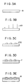
- This method forms the track by utilizing the property of a certain kind of substance that, when such substance is vapor deposited in an extremely minute amount on a substrate, such vapor deposited substance will exhibit selective growth reflecting the micro-structure of the substrate surface. More specifically, when a metal such as gold silver, chromium, cobalt, etc, is vacuum deposited after irradiation of electron beam 101 on a silicon substrate 102 as shown in Figs. 3A and 3B, the existence probability of the vapor deposited substance 102 becomes very small on the track where the electron beam is irradiated (Fig. 3C).
- the beam diameter of the electron beam to be irradiated may be 50 ⁇ or less, and when a track with a wide width is to be prepared, irradiation scanning will be repeated for plural times while deviating little by little the electron beam.
- the width of the track 40 ⁇ to 400 ⁇ may be preferable, more preferably 40 ⁇ to 200 ⁇ .
- the height of the track, namely the film thickness of the vapor deposited product 102, mav be about 25 ⁇ to 1000 ⁇ , preferably 30 ⁇ to 100 ⁇ , more preferably 30 ⁇ to 80 ⁇ .
- the substrate 9 it is required to involve no problem of charging accompanying electron beam irradiation 101, and utilization of silicon wafer, etc. is preferable.
- a metal such as gold, silver, chromium, cobalt, platinum, etc. can be utilized, and since the track width is as small as 40 ⁇ to 400 ⁇ , it is desirable to vapor-deposit ultra-fine particles 102 of these metals.
- the substrate electrode 7 is formed (Fig. 3D).
- the metal constituting the substrate electrode 7 in addition to gold, silver, copper, aluminum, platinum, etc., alloys such as Au-Pd, etc. can be also utilized. Even when any material may be employed, care should be taken so that the groove of the track may not be embedded during formation of the substrate electrode 7, and its surface should be preferably smooth, and it should be desirably formed by the sputtering method, etc.
- the substrate electrode 7 should preferably have a film thickness of 100 ⁇ to 300 ⁇ .
- a recording layer 8 is formed on the substrate electrode 7 (Fig. 3E).
- materials having the memory-switching phenomenon (electrical memory effects) in current-voltage characteristics can be utilized.
- the recording layer has at least two clearly different resistance states, and such states are freely transitionable to each other by application of a voltage or current of the threshold value or higher (switching phenomenon), and also the respective resistance states created can maintain their states in the case of application of a voltage or current within the threshold value (memory phenomenon).
- amorphous semiconductors such as oxide glass, borate glass or chalcogenide glass containing Se, Te, as compounded with the element of the group III, IV, V or VI of the periodic table, etc. They are intrinsic semiconductors having an optical band gap Eg of 0.6 to 1.4 eV or an electrical activation energy ⁇ E of approximately 0.7 to 1.6 eV.
- chalcogenide glass may include A-Se-Te type, Ge-As-Se type, Si-Ge-As-Te type, for example, Si16Ge14As5Te65 (the subscripts show atomic%), or Ge-Te-X type, Si-Te-X type (X represents small amount of group V, and VI elements), for example Ge15Te81Sb2S2. Further, a chalcogenide glass of Ge-Sb-Se type may be also used.
- the electric memory effect of the medium can be exhibited.
- the object of the present invention can be sufficiently accomplished according to the thin-film-forming technique known in the art.
- suitable film-forming methods may include the vacuum vapor deposition method, the cluster ion beam method, etc.
- the electric memory effect of such material is observed at a film thickness of several ⁇ m or less, and concerning recording resolving power as the recording medium, the thickness may be preferably thinner.
- a film thickness is preferably 100 ⁇ to 1 ⁇ m , more preferably a thickness of 1000 ⁇ or less.
- organic semiconductor layers deposited as a salt of an electron accepting compound such as tetraquinodimethane (TCNQ), TCNQ derivatives, for example, tetrafluorotetracyanoquinodimethane (TCNQF4), tetracyanoethylene (TCNE) and tetracyanonaphthoquinodimethane (TNAP), etc. with a metal having relatively lower reduction potential such as copper or silver on the electrode.
- an electron accepting compound such as tetraquinodimethane (TCNQ), TCNQ derivatives, for example, tetrafluorotetracyanoquinodimethane (TCNQF4), tetracyanoethylene (TCNE) and tetracyanonaphthoquinodimethane (TNAP), etc.
- TCNQ tetrafluorotetracyanoquinodimethane
- TCNE tetracyanoethylene
- TNAP tetracyanonaphthoquinodimethane
- the method for forming such organic semiconductor layer there may be employed the method in which the above electron accepting compound is vacuum vapor deposited on the electrode of copper or silver.
- the electric memory effect of such organic semiconductor is observed at a film thickness of several ten ⁇ m or less, but a film thickness of 100 ⁇ to 1 ⁇ m is preferred with respect to film forming property and uniformity.
- a-Si amorphous silicon
- it is a recording medium having a layer constitution of metal/a-Si (p+ layer/n layer/i layer) or metal/a-Si (n+ layer/p layer/i layer), and the respective layers of a-Si can be deposited satisfactorily according to the methods known in the art.
- the glow discharge method (GD) may be preferably employed.
- the film thickness of a-Si may be preferably 2000 ⁇ to 8000 ⁇ for the n layer, about 1000 ⁇ for the p+ layer, with the total film thickness being preferably about 0.5 ⁇ m to 1 ⁇ m.
- a recording layer with a molecule having a group having ⁇ -electron level and a group having only ⁇ -electron level laminated in combination on the electrode layer can be employed (4) a recording layer with a molecule having a group having ⁇ -electron level and a group having only ⁇ -electron level laminated in combination on the electrode layer.
- the structure of the dye having ⁇ -electron system suitable for the present invention there may be included, for example, dyes having porphyrine skeleton such as phthalocyanine, tetraphenylporphyrine, etc.; azulene type dyes having squarylium group and croconic methine group as the bonding chain and cyanine-like dyes having two or more nitrogen-containing heterocyclic rings such as quinoline, benzothiazole, benzoxazole, etc.
- cyanine dyes condensed polycyclic aromatic compounds such as anthracene and pyrene, and chain compounds obtained by polymerization of aromatic ring and heterocyclic compounds; and polymers of diacetylene group; further derivatives of tetraquinodimethane or tetrathiafluvalene and analogues thereof and charge transfer complexes thereof; and further metal complex compounds such as ferrocene, tris-bipyridine ruthenium complexes, polyimide derivatives, polyamic acid derivatives, polyamide derivatives, various fumaric acid copolymers, various maleic acid copolymers, polyacrylic acid derivatives, various acrylic acid copolymers, polydiacetylene derivatives, various vinyl compounds, synthetic polypeptides, biological high molecular weight compounds such as bacteriorhodopsin, cytochrome C, etc.
- an LB method is extremely suitable among the known techniques because of controllability, easiness and reproducibility.
- a monolayer of an organic compound having a hydrophobic site and a hydrophilic site in one molecule or a built-up film thereof can be formed easily on a substrate, which has a thickness on the molecular order and a uniform and homogeneous organic ultra-thin film can be supplied stably over a large area.
- the LB method is a method in which a monolayer or its built-up film is prepared by utilizing the phenomenon that, in a molecule with a structure having a hydrophilic site and a hydrophobic site in a molecule, when the balance of the both (amphiphilic balance) is brought to a proper value, the molecule will form a monolayer on the water surface with the hydrophilic group directed downward.
- Examples of the group constituting the hydrophobic site may include various hydrophobic groups generally known widely such as saturated and unsaturated hydrocarbon groups, condensed polycyclic aromatic groups and chain polycyclic phenyl groups, etc. These may constitute the hydrophobic moiety each individually or as a combination of a plurality thereof.
- most representative as the constituent of the hydrophilic moiety are, for example, hydrophilic groups such as carboxyl group, ester group, acid amide group, imide group, hydroxyl group, further amino groups (primary, secondary, tertiary, and quaternary), etc. These also constitute the hydrophilic moiety of the above molecule each individually or as a combination of a plurality thereof.
- Organic compounds having these hydrophobic groups and hydrophilic groups in combination with good balance and having a ⁇ -electron system having an adequate size can form a monolayer film on the water surface and can be extremely suitable materials for the present invention.
- polymeric compounds or large cyclic compounds such as phthalocyanine, etc. from the standpoint of heat resistance.
- polymeric materials such as polyimides, polyacrylic acids, various fumaric acid copolymers, or various maleic acid copolymers, etc., not only heat resistance is excellent but also the film thickness per one layer can be made about 5 ⁇ .
- the electrical memory effect of these compounds having ⁇ -electron level has been observed for one having a film thickness of some 10 nm or less, but the thickness should be preferably made 5 ⁇ to 300 ⁇ from the standpoints of film forming property and uniformity.
- the tip end of the probe electrode to be used in the present invention is required to be pointed for enhancing the resolving power of recording/reproduction/erasing.
- one with the tip end of tungsten with a thickness of 1 mm ⁇ being mechanically polished to a cone of 90 ° which is then subjected to an electrical field in ultra-high vacuum to vaporize the surface atoms is employed, but the shape of the probe and the treatment method are not limited to these at all.
- the number of the probe electrode is not required to be limited to one, but a plural number of probe electrodes may be employed as separately for position detection and for recording and reproduction, etc.
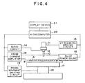
- a probe electrode 10 is used for recording and reproduction, as well as tracking.
- the recording medium to be used is mounted on the XY stage 17.
- a probe current amplifier 15 constitutes a bias voltage application circuit for reproduction.
- a servo circuit 14 controlls the XY direction fine movement control mechanism 11 and the Z direction fine movement control mechanism 12 by use of a piezoelectric element so that the probe current may be constant.
- a pulse power source 16 applies a pulse voltage for recording and erasing between the probe electrode 10 and the substrate electrode 7.
- the servo circuit 14 is controlled to set the HOLD circuit ON so that the output voltage during that period may be constant.
- a XY scanning driving circuit 13 controls the probe electrode movement in the XY direction.
- Rough movement mechanism 18 and rough movement driving circuit 19 are used for rough movement control of the distance between the probe electrode 10 and the recording medium so that a probe current of about 10 ⁇ 1 A may be previously obtained, or for taking a great relative displacement in the XY direction between the probe electrode and the substrate (outside the scope of fine movement control mechanism).
- Z direction fine movement control range 0.1 nm to 1 ⁇ m
- Z direction rough movement control range 10 nm to 10 mm
- XY direction scanning range 0.1 nm to 1 ⁇ m
- XY direction rough movement control range 10 nm to 10 mm
- recording may be also performed by use of a probe electrode by applying a pulse voltage corresponding to recording information on the recording medium of the present invention containing a metal layer such as of gold, etc. and changing partially the shape of said metal layer.
- recording may be effected by making a concavity by bringing the probe electrode into contact with the recording medium.
- recording and reproduction may be effected by utilizing the interatomic force between the scanning probe and the recording medium. In this case, during information recording, the method of voltage application onto the recording medium or contact of the probe is required.
- the recording medium When there is unevenness corresponding to information provided previously in the recording layer of the recording medium, namely when used exclusively for reproduction, the recording medium is not required to have an electroconductive portion (substrate electrode, etc.) but may be constituted only of a complete insulator.
- this scanning probe particularly when its recording density is 1010 bits or higher, the width and/or the pitch ot the track to be used during tracking is required to be sufficiently small corresponding to the size of bit, namely at least some 100 ⁇ or less.
- the solution was spread onto a subphase comprising pure water of a water temperature of 20 °C. After evaporation of the solvent, the surface pressure of the spread film was enhanced to 25 mN/m to form a monolayer on the water surface.
- the substrate equipped with substrate electrode as described above was gently dipped at a speed of 5 mm/min in the direction crossing the surface while maintaining constantly the surface pressure, it was subsequently drawn up gently at a speed of 5 mm/min to prepare a Y type built-up film of two monolayers. By repeating such operation, a 4-layer built-up film of polyamide acid octadecylamine salt was prepared.
- the substrate was calcined by heating under reduced pressure (ca. 1 mm Hg) at 300 °C for 10 minutes to imidate the polyamide acid octadecylamine salt (Formula 3) to obtain a 4-layer polyimide built-up film.
- the recording and reproducing device shown in Fig. 4 was employed.
- the probe electrode 10 a probe electrode made of platinum-rhodium (80:20) was employed.
- the probe electrode 10 is used for controlling the distance (Z) from the surface of the recording layer 8 and the distance (Z) is finely controlled by a piezoelectric element so that the current may be maintained constant.
- the fine movement control mechanism 11 is designed so that fine movement control can be also effected in the interplanar (X,Y) direction while maintaining constantly the distance Z.
- the probe electrode 10 can directly perform recording, reproduction and erasing.
- the recording medium is placed on the XY stage 17 of high precision, and can be moved to any desired position.
- the recording medium having the recording layer 8 with 4-layer built-up polyimide as described above was mounted on the XY stage 17. At this time, it was mounted so that the length direction of the track (Y direction in Fig. 1) and the Y direction of the recording and reproducing device may be substantially in parallel to each other.
- a bias voltage of + 1.5 V was applied between the probe electrode 10 and the substrate electrode 7 of the recording medium, and the distance (Z) between the probe electrode 10 and the surface of the recording layer 8 was adjusted while monitoring the current.
- the probe current Ip for controlling the distance Z between the probe electrode 10 and the surface of the recording layer 8 was set to 10 ⁇ 8 A ⁇ Ip ⁇ 10 ⁇ 10 A.
- the probe electrode 10 was scanned in the X direction, namely the direction crossing the track, and after confirmation that the recording medium surface reflected the shape of the track, the probe electrode 10 was held on any desired track (convexity).
- the probe electrode was scanned in the Y direction.
- the position control in the Z direction was required for maintaining the probe current constant, and when the positional displacement of the probe electrode at the time t + ⁇ t relative of the position of the probe electrode at a certain time t exceeds -5 ⁇ the displacement amount was controlled within -5 ⁇ by scanning the probe electrode in the X or -X direction.
- ⁇ t was set equal to 1 ⁇ s.
- the pitch of electron beam irradiation was made 80 ⁇ and the average film thickness of ultra-fine particles of gold made 30 ⁇ , following otherwise entirely the same procedure, a recording medium was prepared. At this time, the width and the height of the track were respectively about 40 ⁇ and 30 ⁇ .
- the bit error rate was 3 x 10 ⁇ 6.
- Example 1 vapor deposition of ultra-fine particles of gold was changed to silver, and the recording layer was changed from the polyimide to the 4-layer LB film of squarylium-bis-6- octylazulene (hereinafter abbreviated as SOAZ), following otherwise entirely the same procedure as in Example 1, a recording medium was formed.
- SOAZ squarylium-bis-6- octylazulene
- a solution containing SOAZ dissolved at a concentration of 0.2 mg/ml in benzene was spread onto a subphase comprising pure water of 20 °C. After evaporation of the solvent, the surface pressure of the spread film was enhanced to 20 mN/m to form a monolayer on the water surface, and further the above substrate was repeatedly dipped and drawn up at a speed of 3 mm/min in the direction crossing the water surface while maintaining the surface pressure, whereby a built-up film of 4 layers of SOAZ monolayer was formed on the substrate electrode 7.
- the bit error rate was 3 x 10 ⁇ 6.
- the track having a linear shape but the shape is not limited thereto. but other forms such as spiral, circular shape, etc. can be also used without any problem at all.
- the preparation method of the recording layers any film forming method capable of preparing an extremely uniform film may be available, and the method of the present invention is not limitative.
- the present invention is not limited at all with respect to substrate materials. Further, in the present Examples, one probe electrode was employed, but two or more electrodes may be employed as separately for recording and reproduction and for tracking, respectively.
Landscapes
- Semiconductor Memories (AREA)
- Optical Record Carriers And Manufacture Thereof (AREA)
- Thermal Transfer Or Thermal Recording In General (AREA)
- Optical Recording Or Reproduction (AREA)
Applications Claiming Priority (4)
| Application Number | Priority Date | Filing Date | Title |
|---|---|---|---|
| JP205767/89 | 1989-08-10 | ||
| JP20576789 | 1989-08-10 | ||
| JP194977/90 | 1990-07-25 | ||
| JP2194977A JP2859715B2 (ja) | 1989-08-10 | 1990-07-25 | 記録媒体用基板及びその製造方法、記録媒体、記録方法、記録再生方法、記録装置、記録再生装置 |
Publications (3)
| Publication Number | Publication Date |
|---|---|
| EP0412850A2 true EP0412850A2 (de) | 1991-02-13 |
| EP0412850A3 EP0412850A3 (en) | 1991-05-29 |
| EP0412850B1 EP0412850B1 (de) | 1995-03-08 |
Family
ID=26508847
Family Applications (1)
| Application Number | Title | Priority Date | Filing Date |
|---|---|---|---|
| EP90308858A Expired - Lifetime EP0412850B1 (de) | 1989-08-10 | 1990-08-10 | Substrat für Aufzeichnungsmedium, Aufzeichnungsmedium, Verfahren zur Herstellung dergleichen, Aufzeichnungs- und Wiedergabeeinrichtung und Verfahren zur Aufzeichnung, Wiedergabe und Löschen mit Gebrauch von einem solchen Aufzeichnungsmedium |
Country Status (5)
| Country | Link |
|---|---|
| US (1) | US5396483A (de) |
| EP (1) | EP0412850B1 (de) |
| JP (1) | JP2859715B2 (de) |
| CA (1) | CA2022930C (de) |
| DE (1) | DE69017552T2 (de) |
Cited By (6)
| Publication number | Priority date | Publication date | Assignee | Title |
|---|---|---|---|---|
| EP0537642A3 (en) * | 1991-10-15 | 1995-02-15 | Canon Kk | Information processing apparatus with tracking mechanism |
| EP0510579A3 (en) * | 1991-04-24 | 1995-02-15 | Canon Kk | Apparatus for recording and/or reproducing information |
| EP0513790A3 (en) * | 1991-05-15 | 1995-02-15 | Canon Kk | Information processing apparatus |
| EP0416920B1 (de) * | 1989-09-07 | 1996-01-03 | Canon Kabushiki Kaisha | Informationsverarbeitungsverfahren und -vorrichtung |
| EP0441626B1 (de) * | 1990-02-07 | 1998-10-14 | Canon Kabushiki Kaisha | Medium, Herstellungsverfahren desselben, Informationsverarbeitungsvorrichtung und Informationsverarbeitungsverfahren |
| US6308405B1 (en) | 1990-02-07 | 2001-10-30 | Canon Kabushiki Kaisha | Process for preparing an electrode substrate |
Families Citing this family (39)
| Publication number | Priority date | Publication date | Assignee | Title |
|---|---|---|---|---|
| US6339217B1 (en) * | 1995-07-28 | 2002-01-15 | General Nanotechnology Llc | Scanning probe microscope assembly and method for making spectrophotometric, near-field, and scanning probe measurements |
| US6337479B1 (en) * | 1994-07-28 | 2002-01-08 | Victor B. Kley | Object inspection and/or modification system and method |
| US5751683A (en) * | 1995-07-24 | 1998-05-12 | General Nanotechnology, L.L.C. | Nanometer scale data storage device and associated positioning system |
| US6507553B2 (en) | 1995-07-24 | 2003-01-14 | General Nanotechnology Llc | Nanometer scale data storage device and associated positioning system |
| US7102982B1 (en) * | 1997-05-30 | 2006-09-05 | International Business Machines Corporation | Storage apparatus and method utilizing a charge storage layer having discrete conductive charge-storing elements |
| US6752008B1 (en) | 2001-03-08 | 2004-06-22 | General Nanotechnology Llc | Method and apparatus for scanning in scanning probe microscopy and presenting results |
| US7196328B1 (en) | 2001-03-08 | 2007-03-27 | General Nanotechnology Llc | Nanomachining method and apparatus |
| US6802646B1 (en) | 2001-04-30 | 2004-10-12 | General Nanotechnology Llc | Low-friction moving interfaces in micromachines and nanomachines |
| US6923044B1 (en) | 2001-03-08 | 2005-08-02 | General Nanotechnology Llc | Active cantilever for nanomachining and metrology |
| US6787768B1 (en) | 2001-03-08 | 2004-09-07 | General Nanotechnology Llc | Method and apparatus for tool and tip design for nanomachining and measurement |
| JPH11213301A (ja) * | 1998-01-28 | 1999-08-06 | Hitachi Ltd | 記録媒体および記録装置 |
| US7260051B1 (en) | 1998-12-18 | 2007-08-21 | Nanochip, Inc. | Molecular memory medium and molecular memory integrated circuit |
| WO2001003157A1 (en) * | 1999-07-01 | 2001-01-11 | General Nanotechnology, Llc | Object inspection and/or modification system and method |
| US6931710B2 (en) | 2001-01-30 | 2005-08-23 | General Nanotechnology Llc | Manufacturing of micro-objects such as miniature diamond tool tips |
| US7253407B1 (en) | 2001-03-08 | 2007-08-07 | General Nanotechnology Llc | Active cantilever for nanomachining and metrology |
| US20020138301A1 (en) * | 2001-03-22 | 2002-09-26 | Thanos Karras | Integration of a portal into an application service provider data archive and/or web based viewer |
| US7053369B1 (en) * | 2001-10-19 | 2006-05-30 | Rave Llc | Scan data collection for better overall data accuracy |
| US6813937B2 (en) | 2001-11-28 | 2004-11-09 | General Nanotechnology Llc | Method and apparatus for micromachines, microstructures, nanomachines and nanostructures |
| EP1539637A4 (de) * | 2002-09-09 | 2010-07-28 | Gen Nanotechnology Llc | Fluidzufuhr für rastertunnelmikroskopie |
| US7233517B2 (en) | 2002-10-15 | 2007-06-19 | Nanochip, Inc. | Atomic probes and media for high density data storage |
| US20050243592A1 (en) * | 2004-04-16 | 2005-11-03 | Rust Thomas F | High density data storage device having eraseable bit cells |
| US20050243660A1 (en) * | 2004-04-16 | 2005-11-03 | Rust Thomas F | Methods for erasing bit cells in a high density data storage device |
| KR100580651B1 (ko) * | 2004-06-03 | 2006-05-16 | 삼성전자주식회사 | 프로브를 이용한 정보저장시스템의 위치오차 검출 장치 및방법, 이를 이용한 정보저장시스템의 정보 추종 장치 및방법 |
| KR100612857B1 (ko) * | 2004-08-14 | 2006-08-14 | 삼성전자주식회사 | 프로브를 이용한 정보저장시스템의 프로브 위치오차 검출방법 및 장치 |
| US8649249B1 (en) * | 2004-09-02 | 2014-02-11 | Seagate Technology Llc | Printing magnetic pattern onto disk |
| US20060291271A1 (en) * | 2005-06-24 | 2006-12-28 | Nanochip, Inc. | High density data storage devices having servo indicia formed in a patterned media |
| US7367119B2 (en) * | 2005-06-24 | 2008-05-06 | Nanochip, Inc. | Method for forming a reinforced tip for a probe storage device |
| US20070041237A1 (en) * | 2005-07-08 | 2007-02-22 | Nanochip, Inc. | Media for writing highly resolved domains |
| US7463573B2 (en) * | 2005-06-24 | 2008-12-09 | Nanochip, Inc. | Patterned media for a high density data storage device |
| US7309630B2 (en) | 2005-07-08 | 2007-12-18 | Nanochip, Inc. | Method for forming patterned media for a high density data storage device |
| US20070008867A1 (en) * | 2005-07-08 | 2007-01-11 | Nanochip, Inc. | High density data storage devices with a lubricant layer comprised of a field of polymer chains |
| US20070008866A1 (en) * | 2005-07-08 | 2007-01-11 | Nanochip, Inc. | Methods for writing and reading in a polarity-dependent memory switch media |
| US20080175033A1 (en) * | 2007-01-19 | 2008-07-24 | Nanochip, Inc. | Method and system for improving domain stability in a ferroelectric media |
| US20080233672A1 (en) * | 2007-03-20 | 2008-09-25 | Nanochip, Inc. | Method of integrating mems structures and cmos structures using oxide fusion bonding |
| US7792009B2 (en) * | 2007-10-02 | 2010-09-07 | Seagate Technology Llc | Ferroelectric polarization pattern with differing feedback signals |
| US20090092805A1 (en) * | 2007-10-03 | 2009-04-09 | Seagate Technology Llc | Ferroelectric Material With Polarization Pattern |
| US20090129246A1 (en) * | 2007-11-21 | 2009-05-21 | Nanochip, Inc. | Environmental management of a probe storage device |
| FR2925748B1 (fr) * | 2007-12-21 | 2010-01-29 | Commissariat Energie Atomique | Support de stockage de donnees et procede associe |
| US20100039729A1 (en) * | 2008-08-14 | 2010-02-18 | Nanochip, Inc. | Package with integrated magnets for electromagnetically-actuated probe-storage device |
Family Cites Families (25)
| Publication number | Priority date | Publication date | Assignee | Title |
|---|---|---|---|---|
| US4018937A (en) * | 1972-12-14 | 1977-04-19 | Rca Corporation | Electron beam recording comprising polymer of 1-methylvinyl methyl ketone |
| US4133047A (en) * | 1975-02-12 | 1979-01-02 | Cyrus Levinthal | System for storing and retrieving information at the molecular level |
| CH643397A5 (de) * | 1979-09-20 | 1984-05-30 | Ibm | Raster-tunnelmikroskop. |
| JPS6141762A (ja) * | 1984-08-06 | 1986-02-28 | Res Dev Corp Of Japan | 超微細パタ−ンの形成法 |
| JPS6180536A (ja) * | 1984-09-14 | 1986-04-24 | ゼロツクス コーポレーシヨン | 原子規模密度情報記緑および読出し装置並びに方法 |
| GB8526866D0 (en) * | 1985-10-31 | 1985-12-04 | Emi Plc Thorn | Information recovery system |
| JP2616763B2 (ja) * | 1985-12-13 | 1997-06-04 | 新技術事業団 | 情報記録再生方法 |
| JPS62246784A (ja) * | 1986-04-21 | 1987-10-27 | Canon Inc | 光記録媒体 |
| US4760567A (en) * | 1986-08-11 | 1988-07-26 | Electron Beam Memories | Electron beam memory system with ultra-compact, high current density electron gun |
| US4972402A (en) * | 1986-11-20 | 1990-11-20 | Canon Kabushiki Kaisha | Optical card |
| JP2556491B2 (ja) * | 1986-12-24 | 1996-11-20 | キヤノン株式会社 | 記録装置及び記録法 |
| JPS63204531A (ja) * | 1987-02-19 | 1988-08-24 | Canon Inc | 再生装置 |
| DE3752099T2 (de) * | 1986-12-24 | 1997-11-13 | Canon Kk | Aufzeichnungsgerät und Wiedergabegerät |
| JP2556492B2 (ja) * | 1986-12-24 | 1996-11-20 | キヤノン株式会社 | 再生装置及び再生法 |
| JPS63261554A (ja) * | 1987-04-20 | 1988-10-28 | Hitachi Ltd | 情報記憶装置 |
| JP2603270B2 (ja) * | 1987-08-25 | 1997-04-23 | キヤノン株式会社 | 記録装置および再生装置 |
| EP0307211A3 (de) * | 1987-09-10 | 1991-05-15 | Seiko Instruments Inc. | Speicher-Lesegerät |
| EP0307210A3 (de) * | 1987-09-10 | 1991-05-15 | Seiko Instruments Inc. | Speicher-Schreibgerät |
| JPH01116940A (ja) * | 1987-10-29 | 1989-05-09 | Hitachi Ltd | 情報の記録再生方法 |
| JP2523144B2 (ja) * | 1987-11-18 | 1996-08-07 | 株式会社日立製作所 | 情報記録再生装置および情報記録媒体 |
| US4876042A (en) * | 1987-12-28 | 1989-10-24 | Canon Kabushiki Kaisha | Molding processing using a reproducible molding die |
| JP2578459B2 (ja) * | 1988-01-25 | 1997-02-05 | キヤノン株式会社 | 情報記録媒体、情報記録媒体用基板の製造方法及び情報記録媒体用基板の成形用型 |
| JP2756254B2 (ja) * | 1988-03-25 | 1998-05-25 | キヤノン株式会社 | 記録装置及び再生装置 |
| JPH07105067B2 (ja) * | 1988-04-28 | 1995-11-13 | キヤノン株式会社 | 情報記録媒体用基板及びその製造方法 |
| NL8802335A (nl) * | 1988-09-21 | 1990-04-17 | Philips Nv | Werkwijze en inrichting voor het op sub-mikron schaal bewerken van een materiaal-oppervlak. |
-
1990
- 1990-07-25 JP JP2194977A patent/JP2859715B2/ja not_active Expired - Fee Related
- 1990-08-08 CA CA002022930A patent/CA2022930C/en not_active Expired - Fee Related
- 1990-08-10 DE DE69017552T patent/DE69017552T2/de not_active Expired - Fee Related
- 1990-08-10 EP EP90308858A patent/EP0412850B1/de not_active Expired - Lifetime
-
1992
- 1992-11-18 US US07/978,023 patent/US5396483A/en not_active Expired - Fee Related
Cited By (7)
| Publication number | Priority date | Publication date | Assignee | Title |
|---|---|---|---|---|
| EP0416920B1 (de) * | 1989-09-07 | 1996-01-03 | Canon Kabushiki Kaisha | Informationsverarbeitungsverfahren und -vorrichtung |
| EP0441626B1 (de) * | 1990-02-07 | 1998-10-14 | Canon Kabushiki Kaisha | Medium, Herstellungsverfahren desselben, Informationsverarbeitungsvorrichtung und Informationsverarbeitungsverfahren |
| US6308405B1 (en) | 1990-02-07 | 2001-10-30 | Canon Kabushiki Kaisha | Process for preparing an electrode substrate |
| EP0510579A3 (en) * | 1991-04-24 | 1995-02-15 | Canon Kk | Apparatus for recording and/or reproducing information |
| EP0513790A3 (en) * | 1991-05-15 | 1995-02-15 | Canon Kk | Information processing apparatus |
| US5485451A (en) * | 1991-05-15 | 1996-01-16 | Canon Kabushiki Kaisha | Information processing apparatus |
| EP0537642A3 (en) * | 1991-10-15 | 1995-02-15 | Canon Kk | Information processing apparatus with tracking mechanism |
Also Published As
| Publication number | Publication date |
|---|---|
| JP2859715B2 (ja) | 1999-02-24 |
| DE69017552D1 (de) | 1995-04-13 |
| CA2022930A1 (en) | 1991-02-11 |
| EP0412850B1 (de) | 1995-03-08 |
| JPH03156749A (ja) | 1991-07-04 |
| DE69017552T2 (de) | 1995-08-03 |
| EP0412850A3 (en) | 1991-05-29 |
| US5396483A (en) | 1995-03-07 |
| CA2022930C (en) | 1995-02-14 |
Similar Documents
| Publication | Publication Date | Title |
|---|---|---|
| EP0412850B1 (de) | Substrat für Aufzeichnungsmedium, Aufzeichnungsmedium, Verfahren zur Herstellung dergleichen, Aufzeichnungs- und Wiedergabeeinrichtung und Verfahren zur Aufzeichnung, Wiedergabe und Löschen mit Gebrauch von einem solchen Aufzeichnungsmedium | |
| CA2071726C (en) | Recording medium, information-processing apparatus using same, and information-erasing method | |
| US5623476A (en) | Recording device and reproduction device | |
| EP0416920B1 (de) | Informationsverarbeitungsverfahren und -vorrichtung | |
| CA2024648C (en) | Accessing method, and information processing method and information processing device utilizing the same | |
| US6308405B1 (en) | Process for preparing an electrode substrate | |
| US5162819A (en) | Information processing apparatus, information processing method, and recording medium employed therefor | |
| EP0412829B1 (de) | Aufzeichnungsmedium, Verfahren zur Herstellung desselben, Aufzeichnungs- und Wiedergabeeinrichtung und Verfahren zur Aufzeichnung, Wiedergabe und zum Löschen mit einem solchen Aufzeichnungsmedium | |
| EP0475365A2 (de) | Nachführungsmethode für Speichergerät | |
| EP0551965B1 (de) | Aufzeichnungsgerät und Wiedergabegerät | |
| EP0441626B1 (de) | Medium, Herstellungsverfahren desselben, Informationsverarbeitungsvorrichtung und Informationsverarbeitungsverfahren | |
| JPS63204531A (ja) | 再生装置 | |
| JP2866165B2 (ja) | 記録媒体およびその製造方法、情報処理方法、情報処理装置 | |
| JP2782275B2 (ja) | 電極基板及び記録媒体の製造方法 | |
| JP2926522B2 (ja) | 記録媒体及びその製造方法と情報処理装置 | |
| JP2748182B2 (ja) | 記録媒体およびその製造方法、記録方法、記録再生方法、記録装置、再生装置、記録再生装置 | |
| JPH0490151A (ja) | 情報処理方法及び情報処理装置 | |
| JPH05314551A (ja) | 記録媒体製造方法及び記録媒体 | |
| JPH0644619A (ja) | 記録媒体及び記録媒体製造方法 | |
| JPH0512726A (ja) | 記録媒体、およびそれを用いて記録、再生、消去を行う情報処理装置 | |
| JPH03295043A (ja) | 記録媒体 | |
| JPH06111390A (ja) | 記録媒体製造方法 | |
| JPH04143942A (ja) | トラック形成方法 | |
| JPH03295044A (ja) | 記録媒体の製造方法 | |
| JPH03272037A (ja) | 記録媒体及びその製造方法、記録再生装置 |
Legal Events
| Date | Code | Title | Description |
|---|---|---|---|
| PUAI | Public reference made under article 153(3) epc to a published international application that has entered the european phase |
Free format text: ORIGINAL CODE: 0009012 |
|
| AK | Designated contracting states |
Kind code of ref document: A2 Designated state(s): BE CH DE FR GB IT LI NL SE |
|
| 17P | Request for examination filed |
Effective date: 19901231 |
|
| PUAL | Search report despatched |
Free format text: ORIGINAL CODE: 0009013 |
|
| AK | Designated contracting states |
Kind code of ref document: A3 Designated state(s): BE CH DE FR GB IT LI NL SE |
|
| RHK1 | Main classification (correction) |
Ipc: G11B 9/00 |
|
| 17Q | First examination report despatched |
Effective date: 19930524 |
|
| GRAA | (expected) grant |
Free format text: ORIGINAL CODE: 0009210 |
|
| AK | Designated contracting states |
Kind code of ref document: B1 Designated state(s): BE CH DE FR GB IT LI NL SE |
|
| PG25 | Lapsed in a contracting state [announced via postgrant information from national office to epo] |
Ref country code: IT Free format text: LAPSE BECAUSE OF FAILURE TO SUBMIT A TRANSLATION OF THE DESCRIPTION OR TO PAY THE FEE WITHIN THE PRE;WARNING: LAPSES OF ITALIAN PATENTS WITH EFFECTIVE DATE BEFORE 2007 MAY HAVE OCCURRED AT ANY TIME BEFORE 2007. THE CORRECT EFFECTIVE DATE MAY BE DIFFERENT FROM THE ONE RECORDED.SCRIBED TIME-LIMIT Effective date: 19950308 Ref country code: LI Effective date: 19950308 Ref country code: BE Effective date: 19950308 Ref country code: NL Free format text: LAPSE BECAUSE OF FAILURE TO SUBMIT A TRANSLATION OF THE DESCRIPTION OR TO PAY THE FEE WITHIN THE PRESCRIBED TIME-LIMIT Effective date: 19950308 Ref country code: CH Effective date: 19950308 |
|
| REF | Corresponds to: |
Ref document number: 69017552 Country of ref document: DE Date of ref document: 19950413 |
|
| PG25 | Lapsed in a contracting state [announced via postgrant information from national office to epo] |
Ref country code: SE Effective date: 19950608 |
|
| REG | Reference to a national code |
Ref country code: CH Ref legal event code: PL |
|
| ET | Fr: translation filed | ||
| NLV1 | Nl: lapsed or annulled due to failure to fulfill the requirements of art. 29p and 29m of the patents act | ||
| PLBE | No opposition filed within time limit |
Free format text: ORIGINAL CODE: 0009261 |
|
| STAA | Information on the status of an ep patent application or granted ep patent |
Free format text: STATUS: NO OPPOSITION FILED WITHIN TIME LIMIT |
|
| 26N | No opposition filed | ||
| REG | Reference to a national code |
Ref country code: GB Ref legal event code: IF02 |
|
| PGFP | Annual fee paid to national office [announced via postgrant information from national office to epo] |
Ref country code: GB Payment date: 20040727 Year of fee payment: 15 |
|
| PGFP | Annual fee paid to national office [announced via postgrant information from national office to epo] |
Ref country code: FR Payment date: 20040827 Year of fee payment: 15 |
|
| PGFP | Annual fee paid to national office [announced via postgrant information from national office to epo] |
Ref country code: DE Payment date: 20041028 Year of fee payment: 15 |
|
| PG25 | Lapsed in a contracting state [announced via postgrant information from national office to epo] |
Ref country code: GB Free format text: LAPSE BECAUSE OF NON-PAYMENT OF DUE FEES Effective date: 20050810 |
|
| PG25 | Lapsed in a contracting state [announced via postgrant information from national office to epo] |
Ref country code: DE Free format text: LAPSE BECAUSE OF NON-PAYMENT OF DUE FEES Effective date: 20060301 |
|
| GBPC | Gb: european patent ceased through non-payment of renewal fee |
Effective date: 20050810 |
|
| PG25 | Lapsed in a contracting state [announced via postgrant information from national office to epo] |
Ref country code: FR Free format text: LAPSE BECAUSE OF NON-PAYMENT OF DUE FEES Effective date: 20060428 |
|
| REG | Reference to a national code |
Ref country code: FR Ref legal event code: ST Effective date: 20060428 |