EP0413109A2 - Fabrication de plaquettes à circuits imprimés utilisant des polymères conducteurs - Google Patents
Fabrication de plaquettes à circuits imprimés utilisant des polymères conducteurs Download PDFInfo
- Publication number
- EP0413109A2 EP0413109A2 EP90111709A EP90111709A EP0413109A2 EP 0413109 A2 EP0413109 A2 EP 0413109A2 EP 90111709 A EP90111709 A EP 90111709A EP 90111709 A EP90111709 A EP 90111709A EP 0413109 A2 EP0413109 A2 EP 0413109A2
- Authority
- EP
- European Patent Office
- Prior art keywords
- conducting polymer
- substituted
- polymer
- set forth
- printed circuit
- Prior art date
- Legal status (The legal status is an assumption and is not a legal conclusion. Google has not performed a legal analysis and makes no representation as to the accuracy of the status listed.)
- Ceased
Links
Images

Classifications
-
- H—ELECTRICITY
- H05—ELECTRIC TECHNIQUES NOT OTHERWISE PROVIDED FOR
- H05K—PRINTED CIRCUITS; CASINGS OR CONSTRUCTIONAL DETAILS OF ELECTRIC APPARATUS; MANUFACTURE OF ASSEMBLAGES OF ELECTRICAL COMPONENTS
- H05K3/00—Apparatus or processes for manufacturing printed circuits
- H05K3/10—Apparatus or processes for manufacturing printed circuits in which conductive material is applied to the insulating support in such a manner as to form the desired conductive pattern
- H05K3/18—Apparatus or processes for manufacturing printed circuits in which conductive material is applied to the insulating support in such a manner as to form the desired conductive pattern using precipitation techniques to apply the conductive material
- H05K3/188—Apparatus or processes for manufacturing printed circuits in which conductive material is applied to the insulating support in such a manner as to form the desired conductive pattern using precipitation techniques to apply the conductive material by direct electroplating
-
- C—CHEMISTRY; METALLURGY
- C08—ORGANIC MACROMOLECULAR COMPOUNDS; THEIR PREPARATION OR CHEMICAL WORKING-UP; COMPOSITIONS BASED THEREON
- C08G—MACROMOLECULAR COMPOUNDS OBTAINED OTHERWISE THAN BY REACTIONS ONLY INVOLVING UNSATURATED CARBON-TO-CARBON BONDS
- C08G73/00—Macromolecular compounds obtained by reactions forming a linkage containing nitrogen with or without oxygen or carbon in the main chain of the macromolecule, not provided for in groups C08G12/00 - C08G71/00
- C08G73/02—Polyamines
- C08G73/026—Wholly aromatic polyamines
- C08G73/0266—Polyanilines or derivatives thereof
-
- C—CHEMISTRY; METALLURGY
- C25—ELECTROLYTIC OR ELECTROPHORETIC PROCESSES; APPARATUS THEREFOR
- C25D—PROCESSES FOR THE ELECTROLYTIC OR ELECTROPHORETIC PRODUCTION OF COATINGS; ELECTROFORMING; APPARATUS THEREFOR
- C25D5/00—Electroplating characterised by the process; Pretreatment or after-treatment of workpieces
- C25D5/54—Electroplating of non-metallic surfaces
- C25D5/56—Electroplating of non-metallic surfaces of plastics
-
- H—ELECTRICITY
- H05—ELECTRIC TECHNIQUES NOT OTHERWISE PROVIDED FOR
- H05K—PRINTED CIRCUITS; CASINGS OR CONSTRUCTIONAL DETAILS OF ELECTRIC APPARATUS; MANUFACTURE OF ASSEMBLAGES OF ELECTRICAL COMPONENTS
- H05K3/00—Apparatus or processes for manufacturing printed circuits
- H05K3/40—Forming printed elements for providing electric connections to or between printed circuits
- H05K3/42—Plated through-holes or plated via connections
- H05K3/423—Plated through-holes or plated via connections characterised by electroplating method
- H05K3/424—Plated through-holes or plated via connections characterised by electroplating method by direct electroplating
-
- H—ELECTRICITY
- H05—ELECTRIC TECHNIQUES NOT OTHERWISE PROVIDED FOR
- H05K—PRINTED CIRCUITS; CASINGS OR CONSTRUCTIONAL DETAILS OF ELECTRIC APPARATUS; MANUFACTURE OF ASSEMBLAGES OF ELECTRICAL COMPONENTS
- H05K2201/00—Indexing scheme relating to printed circuits covered by H05K1/00
- H05K2201/03—Conductive materials
- H05K2201/032—Materials
- H05K2201/0329—Intrinsically conductive polymer [ICP]; Semiconductive polymer
-
- H—ELECTRICITY
- H05—ELECTRIC TECHNIQUES NOT OTHERWISE PROVIDED FOR
- H05K—PRINTED CIRCUITS; CASINGS OR CONSTRUCTIONAL DETAILS OF ELECTRIC APPARATUS; MANUFACTURE OF ASSEMBLAGES OF ELECTRICAL COMPONENTS
- H05K3/00—Apparatus or processes for manufacturing printed circuits
- H05K3/10—Apparatus or processes for manufacturing printed circuits in which conductive material is applied to the insulating support in such a manner as to form the desired conductive pattern
- H05K3/108—Apparatus or processes for manufacturing printed circuits in which conductive material is applied to the insulating support in such a manner as to form the desired conductive pattern by semi-additive methods; masks therefor
-
- H—ELECTRICITY
- H05—ELECTRIC TECHNIQUES NOT OTHERWISE PROVIDED FOR
- H05K—PRINTED CIRCUITS; CASINGS OR CONSTRUCTIONAL DETAILS OF ELECTRIC APPARATUS; MANUFACTURE OF ASSEMBLAGES OF ELECTRICAL COMPONENTS
- H05K3/00—Apparatus or processes for manufacturing printed circuits
- H05K3/40—Forming printed elements for providing electric connections to or between printed circuits
- H05K3/42—Plated through-holes or plated via connections
- H05K3/425—Plated through-holes or plated via connections characterised by the sequence of steps for plating the through-holes or via connections in relation to the conductive pattern
- H05K3/426—Plated through-holes or plated via connections characterised by the sequence of steps for plating the through-holes or via connections in relation to the conductive pattern initial plating of through-holes in substrates without metal
Definitions
- the present invention relates to a process useful for fabricating printed circuit boards and particularly for the metallization of plated through holes in printed circuit boards. Specifically, the invention relates to the use of a conducting polymer layer for electrolytic metallization of printed circuit boards which eliminates the necessity for precious metal seeds and electroless copper baths in the manufacture of printed circuit boards.
- Prior art processes for the metallization of plated through holes have usually included the step of seeding or using a catalyst, usually a noble metal salt, within the plated through hole.
- the next step has been to immerse the seeded circuit board in an electroless bath, usually copper, in order to plate a thin layer of copper, approximately 2 to 5 microns thick, in the plated through hole.
- the thin copper layer renders the plated through holes sufficiently conductive so that a thicker copper layer may be added by conventional electrolytic deposition.
- Electroless baths are unstable and require close monitoring and control. Electroless copper baths fluctuate between being too stable resulting in plated through hole voids and being too active which results in homogeneous decomposition of the bath.
- formaldehyde which is probably the most commonly used reducing agent today in electroless copper baths is toxic and poses difficulties in waste treatment and disposal.
- precious metal seeds are expensive and often have a limited useful lifetime.
- a plated through hole is coated using a conductive colloidal graphite suspension (Black Hole Process, Olin Hunt Specialty Products). Once coated, the plated through hole is plated electrolytically , thus eliminating the need for electroless metal deposition.
- the described process is only useful for the plated through holes and is not extendable to plating extended printed circuit board surfaces. Therefore, while the described process is of value for full panel plating by subtractive processing, it is of limited use for pattern electroplating.
- the present invention concerns an electrically conductive polymer coating which may be applied to a printed circuit board composite substrate.
- the polymer coating is applied from a non-aqueous or aqueous solvent followed by an electroplating process that is performed in an aqueous solution.
- the polymer coating is stable in air since the polymer may be cast, painted, spin-coated or dip-coated onto a substrate and may even be removed from the substrate to generate a pattern.
- the polymer coating in practicing the present invention covers a predetermined region of the printed circuit board varying from covering the entire substrate surface including any through hole, blind holes or vias to just coating any through holes, blind holes or vias.
- the polymer is sufficiently conductive that the composite may be electrolytically plated simply by immersion into a copper ion solution, such as a copper sulfate bath.
- the polymer film precludes the need for both precious metal seeds and electroless copper deposition prior to electrolytic metallization.
- pattern electroplating using a thin film of conducting polymer according to the teachings of the present invention permits enhanced circuit line profiles which is an important consideration in fine line circuitization.
- Polymers useful for the electrolytic metallization of printed circuit boards include substituted and unsubstituted polyanilines, substituted polyparaphenylenevinylenes, substituted and unsubstituted polythiophenevinylene, substituted and unsubstituted polyfuranevinylene, substituted and unsubstituted polypyrrolevinylene, substituted and unsubstituted polythiophenes, polyazines, substituted polyfuranes, substituted polyselenophenes, substituted and unsubstituted poly-p-phenylene sulfides and polyacetylenes formed from soluble precursors.
- the preferred polymers for the electrolytic metallization of printed circuit boards is polyaniline.
- a major advantage for the use of the polymer polyaniline in fabricating printed circuit boards according to the present invention is the relatively low cost of producing the polymer.
- a principal object of the present invention is therefore the provision of fabricating printed circuit boards using a conducting polymer film.
- Another object of the present invention is the provision of fabricating printed circuit boards without the necessity of electroless metal baths and precious metal seeds.
- Another object of the present invention is the provision of fabricating printed circuit boards using a conductive polymer which permits metallization of plated through holes, blind holes or vias and the printed circuit board surface.
- a further object of the present invention is the provision of pattern electroplating printed circuit boards in a manner for enhancing circuit line profiles for fine line circuitization.
- a flow diagram of a conventional prior art process for fabricating a printed circuit board begins with a foil clad laminate or substrate at step 12, a hole or pattern of holes to be plated are drilled into the laminate and cleaned in step 14. A precious metal seed layer is applied to the drilled and cleaned hole in step 16. Electroless metal plating in a metal ion bath, such as a copper sulfate/EDTA/formaldehyde bath, provides a thin layer of metal in the through hole in step 18. Photoresist is applied to the plated laminate in step 20 followed by expose and develop. Copper pattern electroplating of the through hole and printed circuit board assembly is achieved at step 22. A metal mask is applied in step 24 and the resist is stripped in step 26. A copper base is etched in step 28. The metal mask is stripped away in step 30.
- a metal ion bath such as a copper sulfate/EDTA/formaldehyde bath
- the circuit line profile of a metallized conductor on a laminate or substrate when practicing the prior art fabrication method contains a foil clad laminate or substrate 32, a superposed thin copper layer 34 applied during electroless metal plat ing, and a superposed thicker layer of electroplated copper 35.
- the thickness of copper layer 34 is in the range between 5 and 15 microns.
- the thickness of copper layer 35 is in the range between 15 and 50 microns.
- the process according to the present invention commences at step 36 by providing a laminate or substrate without a foil clad.
- a hole or pattern of holes which may be through holes, blind holes or vias, are drilled through the laminate and cleaned in step 38.
- a conducting polymer is applied to predetermined locations such as circuit conductors and to the drilled and cleaned holes.
- Photoresist is applied in step 42 followed by expose and develop. Copper pattern electroplating upon the conducting polymer is performed in step 44.
- the resist is stripped away in step 46.
- step 48 the polymer is etched.
- the circuit line or conductor profile when practicing the present invention is shown in Fig. 3B comprising a laminate or substrate 50 without foil clad, a thin conducting polymer layer 52 superposed at predetermined locations such as through holes and circuit conductors on the laminate 50, and a thicker layer of electroplated copper 54 superposed on the polymer layer 52.
- the thickness of the polymer layer is typically in the range between 0.5 and 10 microns.
- the thickness of the electroplated copper layer is typically in the range between 8 and 50 microns.
- the conducting polymer When practicing the process of the present invention the conducting polymer is applied in a manner to cover a predetermined area of the printed circuit board ranging from the entire laminate surface including the plated through holes to only plated through holes.
- the use of a foil clad laminate as in the conventionally known process is obviated by virtue of the laminate surfaces being rendered conductive by the polymer.
- the polymer selected must be sufficiently conductive that the composite may be electrolytically plated by immersion into a copper sulfate, or other metallic ion, solution. In this manner the need for a precious metal seed and for electroless copper plating prior to electrolytic metallization is also obviated.
- pattern electroplating using thin films of conducting polymers permits enhanced circuit line profiles, which is important in fine line circuitization.
- Conducting polymers consist of a series of conjugated polymers which can be converted from an insulating or semiconducting regime to a metallic regime through chemical or electrochemical doping (oxidation for p-doping and reduction for n-doping or acid doping).
- oxidation for p-doping and reduction for n-doping or acid doping As best known today, only p-doped conducting polymer are stable in air. Therefore, the present invention will discuss only p-doped conducting polymers. However, air stable n-doped conducting polymers would also be useful for practicing the present invention.
- these p-doped air stable conducting polymers exhibit conducting characteristics only within certain pH and potential ranges. That is, there is a potential "window" defining a range within which each polymer is rendered conducting. When the potential is below the range, the polymer will be non-conducting and at a potential above the range, the polymer will decompose.
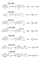
- Figs. 4A to 4G show the chemical diagram and conducting (redox) potential of selected polymers.
- Fig. 4A is a schematic representation of the electro chemically synthesized polymer polypyrrole having a E1 ⁇ 2 potential of -0.20 volts.
- Fig. 4B is a schematic representative of the polymer polyacetylene having a E1 ⁇ 2 potential of 0.17 volts.
- Fig. 4C is a schematic representation of the electrochemically synthesized polymer polythiophene having a E1 ⁇ 2 potential of 0.96 volts.
- Fig. 4D is a schematic representation of the polymer poly-3-methylthiophene having a E1 ⁇ 2 potential of 0.59 volts.
- Fig. 4E is a schematic representation of the polymer poly-3-butylthiophene having a E1 ⁇ 2 potential of 0.78 volts.
- Fig. 4F is a schematic representation of the polymer polythiophene vinylene having a E1 ⁇ 2 potential of 0.19 volts.
- Fig. 4G is a schematic representation of the polymer polyaniline having a E1 ⁇ 2 potential of 0.11 volts. In Figs.
- the value of q is in the range between 0.10 and 0.50.
- the value E1 ⁇ 2 is the average of the anodic peak potential and the cathodic peak potential obtained from cyclic voltammetric studies found in the literature.
- the potential range in which the polymer will be conducting is approximately between E1 ⁇ 2 -0.3V and E1 ⁇ 2 +0.3V. In practice, most conducting polymers will exist at much larger potential ranges than that mentioned above.
- the redox potential of the reaction for copper from the electrochemical series table is 0.3402V vs. NHE (normal hydrogen electrode) or 0.0982V vs. SCE (standard calomel electrode).
- the redox potential of the reaction for copper from the electrochemical series table is 0.3402V vs. NHE (normal hydrogen electrode) or 0.0982V vs. SCE (standard calomel electrode).
- polypyrrole is quite conductive at this potential, however polypyrrole is not suitable for practicing the present invention because it is nonsoluble. While polyalkylthiophenes are soluble, they have slightly higher redox potentials. Therefore, the preferred polymer for the electrolytic metallization of printed circuit boards is polyaniline.
- polyaniline is the preferred conducting polymer, similar results are achievable using other soluble air stable conducting polymers.
- the low cost of producing polyaniline is another advantage to its use in the process of fabrication printed circuit boards. Successful electroplating of copper on epoxy substrates containing a thin layer of polyaniline has been demonstrated.
- the polyaniline After casting polyaniline on an epoxy substrate the polyaniline exhibits a much lower potential than the redox potential of certain precious metals such as Ag/Ag+ and Pd/Pd2+.
- certain precious metals such as Ag/Ag+ and Pd/Pd2+.
- spontaneous plating of Pd and Ag thin film on polyaniline occurs without the introduction of a reducing agent in the electrolyte.
- the thin metallic layer so plated can then be used as an electrode for subsequent electroplating of copper. While this approach does not preclude the use of a precious metal as a base conducting layer it has advantages over existing precious metal seed processes.
- the precious metal may be applied from a simple salt solution of the metal and avoids the use of expensive and unstable precious metal colloids. Further, no subsequent activation step is required for the precious metal prior to electrolytic plating of copper or other metals.
- An epoxy substrate (approximately 0.052 m x 0.052 m (2" x 2")) was first rinsed for several seconds with acetone then rinsed with distilled water. After the described cleaning, the epoxy substrate was blown dry in a nitrogen stream. Polyaniline (emeraldine base) was dissolved in 80% acetic acid and pasted on the cleaned and dried epoxy substrate at a temperature of approximately 100 to 110 degrees centigrade to a thickness of approximately 1 to 2 microns. By virtue of the described treatment the emeraldine base is converted to a conducting emeraldine salt. The conductivity of the coating was approximately 0.3 S/cm as measured by the 4-probe method.
- the epoxy substrate with a polyaniline coating was transferred to 250 ml of a electrolyte solution containing saturated copper sulfate (30g of CuSO4 in 250 ml of water).
- a piece of copper plate was used as a counter electrode and a 100 mA cathodic current was applied to the polyaniline working electrode by a PAR model 273 potentiostat.
- an alligator clip in slight contact with the solution was coupled to the polyaniline coated epoxy substrate.
- Bright copper film was deposited at the contact point between the clip and the polyaniline coating immediately upon application of the cathodic current.
- the area of the copper film continuously grew and spread outward while the cathodic current continued to be applied until the entire area covered with the polyaniline coating was covered with copper. After the entire area was covered with copper film, the current was maintained to increase the thickness of the copper film deposit.
- Pure copper sulfate solution has a pH value in the range between 4 and 5.
- the pH value of the above described electrolyte was measured by pH paper to be approximately 3.
- the different pH is believed to be a result of the partial deprotonation of emeraldine hydroacetate during the experiment. It is known that polyaniline in its emeraldine oxidation state remains electroactive and electrically conductive when the electrolyte pH is less than 4. Therefore, the polyaniline polymer in the experimental conditions described remains electroactive and electrically conductive.
- Example III Spontaneous Plating of Pd Film on Polyaniline Coat from N-Methylpyrrolidinone (NMP)
- Polyaniline (emeraldine base) was dissolved in NMP and the resulting polymer solution was cast on the surface of an epoxy substrate. The assembly was then heated to a temperature of approximately 120 to 130 degrees Centigrade in order to evaporate the NMP solvent. The dried assembly was dipped into an aqueous solution containing 0.05 M palladium chloride and 0.06 M hydrochloric acid. A thin palladium film slowly plated onto the polyaniline polymer surface.
- Example IV Electroplating of Cu on Pd/Polyaniline.
- Polyaniline (emeraldine base or emeraldine salt) was dissolved in pyrrolidine and then painted onto an epoxy substrate at a temperature of approximately 90 to 100 degrees Centigrade while on a hot plate in an exhaust hood.
- the pyrrolidine evaporated within a few seconds after painting and all that remained was a thin coating of the polymer.
- the above described painting process was repeated several times until a copper glint color appeared on the surface.
- the epoxy substrate covered with the polyaniline polymer coating was maintained on the hot plate for an additional 10 to 15 minute period to remove by evaporation any residue pyrrolidine solvent.
- the entire assembly was then dipped into an aqueous solution containing 0.01 M palladium chloride and 0.012 M hydrochloric acid (or 0.05 M palladium chloride and 0.06 M hydrochloric acid).
- a shiny metallic Pd film slowly formed on the polyaniline surface.
- electroplating of copper was performed on the epoxy substrate - polyaniline polymer - Pd assembly under the same conditions as described in Example II.
- Bright copper film was plated homogeneously on the entire palladium surface immediately upon the application of a cathodic current to the assembly. The thickness of the Cu film increased while the cathodic current continued to be applied.
- Polyaniline (emeraldine base) was dissolved in pyrrolidine and the solution was then applied to the surface of an epoxy substrate as described in Example III above.
- the epoxy substrate covered with the polyaniline polymer coating was transferred into a 200 ml aqeous solution containing 1.40g of silver toluene sulfonate and 0.76g of toluene sulfonic acid.
- a thin layer of Ag film slowly began to appear on the surface of the polyaniline polymer.
- Example VI Electroplating of Cu on Polyaniline - Graphite Composition
- a polyaniline coating on an epoxy substrate was prepared as described in Example II above, except that a graphite suspension was mixed with the polyaniline in 80% acetic acid.
- a cathodic current to the polyaniline - graphite composite coating, copper immediately plated at the contact point of the alligator clip and spread to the entire surface of the coating at a faster speed than in Example II. It is believed that the increased spread is due to the increased conductivity of the polyaniline polymer achieved by the inclusion of graphite.
- a conducting polymer such as those described above containing a substance which decomposes upon being exposed to a source of energy for producing a dopant for the polymer is disposed onto a substrate and a predetermined region of the polymer is exposed to a source of energy.
- the region exposed to the source of energy is rendered conductive for subsequent plating according to the present invention.
- Preferred sources of energy include electromagnetic radiation, an electron beam and heat.
- Preferred substances to the conducting polymer are triflate salts, borate salts, and tosylates salts for heat sources of energy and onium salts, iodonium salts, and sulfonyloxyimides for an electromagnetic radiation source of energy such as UV radiation and E-beam radiation, as described in U.S. Patent Application Serial No. 07/357,565.
- the predetermined region is preferably a pattern of conductors.
Landscapes
- Engineering & Computer Science (AREA)
- Chemical & Material Sciences (AREA)
- Organic Chemistry (AREA)
- Chemical Kinetics & Catalysis (AREA)
- Microelectronics & Electronic Packaging (AREA)
- Manufacturing & Machinery (AREA)
- Materials Engineering (AREA)
- Metallurgy (AREA)
- Electrochemistry (AREA)
- Health & Medical Sciences (AREA)
- Medicinal Chemistry (AREA)
- Polymers & Plastics (AREA)
- Manufacturing Of Printed Wiring (AREA)
- Electroplating Methods And Accessories (AREA)
- Printing Elements For Providing Electric Connections Between Printed Circuits (AREA)
- Manufacturing Of Printed Circuit Boards (AREA)
Applications Claiming Priority (2)
| Application Number | Priority Date | Filing Date | Title |
|---|---|---|---|
| US393605 | 1989-08-14 | ||
| US07/393,605 US5300208A (en) | 1989-08-14 | 1989-08-14 | Fabrication of printed circuit boards using conducting polymer |
Publications (2)
| Publication Number | Publication Date |
|---|---|
| EP0413109A2 true EP0413109A2 (fr) | 1991-02-20 |
| EP0413109A3 EP0413109A3 (en) | 1991-07-03 |
Family
ID=23555453
Family Applications (1)
| Application Number | Title | Priority Date | Filing Date |
|---|---|---|---|
| EP19900111709 Ceased EP0413109A3 (en) | 1989-08-14 | 1990-06-21 | Fabrication of printed circuit boards using conducting polymer |
Country Status (3)
| Country | Link |
|---|---|
| US (1) | US5300208A (fr) |
| EP (1) | EP0413109A3 (fr) |
| JP (1) | JPH0799790B2 (fr) |
Cited By (11)
| Publication number | Priority date | Publication date | Assignee | Title |
|---|---|---|---|---|
| US5225495A (en) * | 1991-07-10 | 1993-07-06 | Richard C. Stewart, II | Conductive polymer film formation using initiator pretreatment |
| DE4412463A1 (de) * | 1994-04-08 | 1995-10-12 | Atotech Deutschland Gmbh | Palladiumkolloid-Lösung und deren Verwendung |
| DE19502988A1 (de) * | 1995-01-31 | 1996-08-08 | Univ Dresden Tech | Verfahren zur galvanischen Beschichtung von Polymeroberflächen |
| EP0731192A1 (fr) * | 1995-03-10 | 1996-09-11 | Shipley Company LLC | Procédé et méthode d'électrodéposition |
| US5597471A (en) * | 1992-08-20 | 1997-01-28 | Atotech Deutschland Gmbh | Solution for coating non-conductors with conductive polymers and their metallization process |
| EP0830054A1 (fr) * | 1996-09-12 | 1998-03-18 | Bayer Ag | Procédé de fabrication de circuits rigides et flexibles |
| EP0892089A3 (fr) * | 1997-07-18 | 2001-10-24 | Fuji Photo Film Co., Ltd. | Procédé de fabrication de materiau métallisé |
| WO2002027074A1 (fr) * | 2000-09-26 | 2002-04-04 | Enthone-Omi (Deutschland) Gmbh | Procede de metallisation selective de materiaux dielectriques |
| US6962642B2 (en) | 2002-09-26 | 2005-11-08 | International Business Machines Corporation | Treating copper surfaces for electronic applications |
| EP1976352A4 (fr) * | 2006-01-27 | 2009-12-02 | Sankyo Kasei Kk | Procédé de constitution d'un circuit électroconducteur |
| CN110253703A (zh) * | 2019-05-07 | 2019-09-20 | 杭州电子科技大学 | 一种高强度抑菌木材的制备方法及高强度抑菌木材 |
Families Citing this family (64)
| Publication number | Priority date | Publication date | Assignee | Title |
|---|---|---|---|---|
| US5532025A (en) * | 1993-07-23 | 1996-07-02 | Kinlen; Patrick J. | Corrosion inhibiting compositions |
| US5415762A (en) * | 1993-08-18 | 1995-05-16 | Shipley Company Inc. | Electroplating process and composition |
| US5917229A (en) | 1994-02-08 | 1999-06-29 | Prolinx Labs Corporation | Programmable/reprogrammable printed circuit board using fuse and/or antifuse as interconnect |
| US5572409A (en) | 1994-02-08 | 1996-11-05 | Prolinx Labs Corporation | Apparatus including a programmable socket adapter for coupling an electronic component to a component socket on a printed circuit board |
| US5834824A (en) | 1994-02-08 | 1998-11-10 | Prolinx Labs Corporation | Use of conductive particles in a nonconductive body as an integrated circuit antifuse |
| US5537108A (en) * | 1994-02-08 | 1996-07-16 | Prolinx Labs Corporation | Method and structure for programming fuses |
| US5726482A (en) | 1994-02-08 | 1998-03-10 | Prolinx Labs Corporation | Device-under-test card for a burn-in board |
| US5808351A (en) | 1994-02-08 | 1998-09-15 | Prolinx Labs Corporation | Programmable/reprogramable structure using fuses and antifuses |
| US5813881A (en) | 1994-02-08 | 1998-09-29 | Prolinx Labs Corporation | Programmable cable and cable adapter using fuses and antifuses |
| JPH07321461A (ja) * | 1994-05-25 | 1995-12-08 | Nec Toyama Ltd | 印刷配線板の製造方法 |
| US5700398A (en) * | 1994-12-14 | 1997-12-23 | International Business Machines Corporation | Composition containing a polymer and conductive filler and use thereof |
| US5641841A (en) * | 1995-01-10 | 1997-06-24 | International Business Machines Corporation | Conductive lubricant for magnetic disk drives |
| US5962815A (en) | 1995-01-18 | 1999-10-05 | Prolinx Labs Corporation | Antifuse interconnect between two conducting layers of a printed circuit board |
| US6210537B1 (en) * | 1995-06-19 | 2001-04-03 | Lynntech, Inc. | Method of forming electronically conducting polymers on conducting and nonconducting substrates |
| US5545308A (en) * | 1995-06-19 | 1996-08-13 | Lynntech, Inc. | Method of using conductive polymers to manufacture printed circuit boards |
| US5906042A (en) | 1995-10-04 | 1999-05-25 | Prolinx Labs Corporation | Method and structure to interconnect traces of two conductive layers in a printed circuit board |
| US5767575A (en) | 1995-10-17 | 1998-06-16 | Prolinx Labs Corporation | Ball grid array structure and method for packaging an integrated circuit chip |
| JP3208735B2 (ja) * | 1995-11-29 | 2001-09-17 | ツィッパーリング ケスラー ウント コー (ゲーエムベーハー ウント コー) | 金属化物質の製造方法 |
| US5872338A (en) | 1996-04-10 | 1999-02-16 | Prolinx Labs Corporation | Multilayer board having insulating isolation rings |
| US5980723A (en) * | 1997-08-27 | 1999-11-09 | Jude Runge-Marchese | Electrochemical deposition of a composite polymer metal oxide |
| US6034427A (en) | 1998-01-28 | 2000-03-07 | Prolinx Labs Corporation | Ball grid array structure and method for packaging an integrated circuit chip |
| US20100044080A1 (en) * | 1999-08-27 | 2010-02-25 | Lex Kosowsky | Metal Deposition |
| US7695644B2 (en) | 1999-08-27 | 2010-04-13 | Shocking Technologies, Inc. | Device applications for voltage switchable dielectric material having high aspect ratio particles |
| US20100044079A1 (en) * | 1999-08-27 | 2010-02-25 | Lex Kosowsky | Metal Deposition |
| US20080035370A1 (en) * | 1999-08-27 | 2008-02-14 | Lex Kosowsky | Device applications for voltage switchable dielectric material having conductive or semi-conductive organic material |
| WO2001017320A1 (fr) * | 1999-08-27 | 2001-03-08 | Lex Kosowsky | Structure de transport du courant par un materiau dielectrique a commutation de tension |
| US7825491B2 (en) * | 2005-11-22 | 2010-11-02 | Shocking Technologies, Inc. | Light-emitting device using voltage switchable dielectric material |
| US7446030B2 (en) * | 1999-08-27 | 2008-11-04 | Shocking Technologies, Inc. | Methods for fabricating current-carrying structures using voltage switchable dielectric materials |
| US6334965B1 (en) | 1999-09-07 | 2002-01-01 | Lynntech, Inc. | Electronically conductive polymers |
| JP3379755B2 (ja) | 2000-05-24 | 2003-02-24 | インターナショナル・ビジネス・マシーンズ・コーポレーション | 金属めっき装置 |
| US7404981B2 (en) | 2003-04-21 | 2008-07-29 | Hewlett-Packard Development Company, L.P. | Printing electronic and opto-electronic circuits |
| US7063762B2 (en) * | 2003-08-20 | 2006-06-20 | Endicott Interconnect Technologies, Inc. | Circuitized substrate and method of making same |
| US7279268B2 (en) * | 2004-09-09 | 2007-10-09 | Intel Corporation | Conductive lithographic polymer and method of making devices using same |
| US7923844B2 (en) * | 2005-11-22 | 2011-04-12 | Shocking Technologies, Inc. | Semiconductor devices including voltage switchable materials for over-voltage protection |
| US20100264224A1 (en) * | 2005-11-22 | 2010-10-21 | Lex Kosowsky | Wireless communication device using voltage switchable dielectric material |
| US7981325B2 (en) * | 2006-07-29 | 2011-07-19 | Shocking Technologies, Inc. | Electronic device for voltage switchable dielectric material having high aspect ratio particles |
| US20080032049A1 (en) * | 2006-07-29 | 2008-02-07 | Lex Kosowsky | Voltage switchable dielectric material having high aspect ratio particles |
| US20080029405A1 (en) * | 2006-07-29 | 2008-02-07 | Lex Kosowsky | Voltage switchable dielectric material having conductive or semi-conductive organic material |
| WO2008036423A2 (fr) * | 2006-09-24 | 2008-03-27 | Shocking Technologies, Inc. | Matériau diélectrique commutable par application de tension à réponse graduée en tension, et son procédé de fabrication |
| KR100797708B1 (ko) * | 2006-10-24 | 2008-01-23 | 삼성전기주식회사 | 인쇄회로기판의 제조방법 |
| US20120119168A9 (en) * | 2006-11-21 | 2012-05-17 | Robert Fleming | Voltage switchable dielectric materials with low band gap polymer binder or composite |
| KR100832641B1 (ko) * | 2007-01-03 | 2008-05-27 | 삼성전기주식회사 | 인쇄회로기판의 제조방법 |
| US7793236B2 (en) * | 2007-06-13 | 2010-09-07 | Shocking Technologies, Inc. | System and method for including protective voltage switchable dielectric material in the design or simulation of substrate devices |
| US8206614B2 (en) * | 2008-01-18 | 2012-06-26 | Shocking Technologies, Inc. | Voltage switchable dielectric material having bonded particle constituents |
| JP2009191298A (ja) * | 2008-02-12 | 2009-08-27 | Noritake Co Ltd | 金属微粒子分散液の製造方法 |
| US8203421B2 (en) * | 2008-04-14 | 2012-06-19 | Shocking Technologies, Inc. | Substrate device or package using embedded layer of voltage switchable dielectric material in a vertical switching configuration |
| US20100047535A1 (en) * | 2008-08-22 | 2010-02-25 | Lex Kosowsky | Core layer structure having voltage switchable dielectric material |
| WO2010033635A1 (fr) * | 2008-09-17 | 2010-03-25 | Shocking Technologies, Inc. | Matériau diélectrique commutable en tension contenant un composé de bore |
| US9208931B2 (en) * | 2008-09-30 | 2015-12-08 | Littelfuse, Inc. | Voltage switchable dielectric material containing conductor-on-conductor core shelled particles |
| EP2342722A2 (fr) * | 2008-09-30 | 2011-07-13 | Shocking Technologies Inc | Matériau diélectrique commutable en tension contennant des particules de type noyau enveloppe |
| US8362871B2 (en) * | 2008-11-05 | 2013-01-29 | Shocking Technologies, Inc. | Geometric and electric field considerations for including transient protective material in substrate devices |
| US8272123B2 (en) | 2009-01-27 | 2012-09-25 | Shocking Technologies, Inc. | Substrates having voltage switchable dielectric materials |
| US9226391B2 (en) | 2009-01-27 | 2015-12-29 | Littelfuse, Inc. | Substrates having voltage switchable dielectric materials |
| US8399773B2 (en) | 2009-01-27 | 2013-03-19 | Shocking Technologies, Inc. | Substrates having voltage switchable dielectric materials |
| WO2010110909A1 (fr) | 2009-03-26 | 2010-09-30 | Shocking Technologies, Inc. | Composants comportant des matériaux diélectriques commutables en tension |
| US9053844B2 (en) * | 2009-09-09 | 2015-06-09 | Littelfuse, Inc. | Geometric configuration or alignment of protective material in a gap structure for electrical devices |
| US20110198544A1 (en) * | 2010-02-18 | 2011-08-18 | Lex Kosowsky | EMI Voltage Switchable Dielectric Materials Having Nanophase Materials |
| US9320135B2 (en) * | 2010-02-26 | 2016-04-19 | Littelfuse, Inc. | Electric discharge protection for surface mounted and embedded components |
| US9082622B2 (en) | 2010-02-26 | 2015-07-14 | Littelfuse, Inc. | Circuit elements comprising ferroic materials |
| US9224728B2 (en) * | 2010-02-26 | 2015-12-29 | Littelfuse, Inc. | Embedded protection against spurious electrical events |
| EP2453471A3 (fr) * | 2010-11-15 | 2013-05-15 | Dyconex AG | Procédé de séparation galvanique d'une électrode sur un substrat diélectrique |
| US10151035B2 (en) | 2016-05-26 | 2018-12-11 | Rohm And Haas Electronic Materials Llc | Electroless metallization of through-holes and vias of substrates with tin-free ionic silver containing catalysts |
| KR101951094B1 (ko) * | 2017-02-23 | 2019-05-10 | 인천대학교 산학협력단 | 금속 배선 공정을 위한 폴리아닐린 씨앗층 형성방법 |
| US11332830B2 (en) | 2017-11-15 | 2022-05-17 | Global Graphene Group, Inc. | Functionalized graphene-mediated metallization of polymer article |
Family Cites Families (21)
| Publication number | Priority date | Publication date | Assignee | Title |
|---|---|---|---|---|
| ES316614A1 (es) * | 1964-08-24 | 1966-07-01 | Gen Electric | Un procedimiento para preparar una composicion electronicamente conductora. |
| US3963590A (en) * | 1975-02-25 | 1976-06-15 | E. I. Du Pont De Nemours And Company | Process for electroplating polyoxymethylene |
| US4217183A (en) * | 1979-05-08 | 1980-08-12 | International Business Machines Corporation | Method for locally enhancing electroplating rates |
| DE3014041C2 (de) * | 1980-04-11 | 1982-04-08 | Braun Ag, 6000 Frankfurt | Verfahren zur Aufbringung von elektrisch leitenden Bahnen auf einen Träger aus Isolierstoff |
| US4325780A (en) * | 1980-09-16 | 1982-04-20 | Schulz Sr Robert M | Method of making a printed circuit board |
| DE3132218A1 (de) * | 1981-08-14 | 1983-03-03 | Basf Ag, 6700 Ludwigshafen | Verfahren zur abscheidung von metallen auf elektrisch leitfaehigen, polymeren traegern und verwendung der erhaltenen materialien in der elektrotechnik, zur antistatischen ausruestung von kunststoffen und als heterogene katalysatoren |
| JPS594878A (ja) * | 1982-06-29 | 1984-01-11 | 井関農機株式会社 | 穀粒乾燥機におけるバ−ナの燃焼制御装置 |
| US4532015A (en) * | 1982-08-20 | 1985-07-30 | Phillips Petroleum Company | Poly(arylene sulfide) printed circuit boards |
| US4559112A (en) * | 1983-10-07 | 1985-12-17 | Nippon Telegraph & Telephone | Electrically conducting polymer film and method of manufacturing the same |
| GB2148608B (en) * | 1983-10-22 | 1987-03-18 | Stc Plc | Forming conductive regions in polymeric materials |
| US4486463A (en) * | 1983-12-21 | 1984-12-04 | Gte Laboratories, Incorporated | Selective metal plating onto poly(phenylene sulfide) substrates |
| US4615907A (en) * | 1984-11-23 | 1986-10-07 | Phillips Petroleum Company | Plating poly(arylene sulfide) surfaces |
| JPS61159413A (ja) * | 1984-11-30 | 1986-07-19 | Polyplastics Co | 導電性樹脂複合体の製造方法 |
| US4605471A (en) * | 1985-06-27 | 1986-08-12 | Ncr Corporation | Method of manufacturing printed circuit boards |
| JPS6223195A (ja) * | 1985-07-23 | 1987-01-31 | 日本写真印刷株式会社 | 導電性回路基板とその製造法 |
| US4691091A (en) * | 1985-12-31 | 1987-09-01 | At&T Technologies | Direct writing of conductive patterns |
| JPS6333895A (ja) * | 1986-07-29 | 1988-02-13 | キヤノン株式会社 | 電気回路の製造方法 |
| US4783243A (en) * | 1986-12-18 | 1988-11-08 | American Cyanamid Company | Articles comprising metal-coated polymeric substrates and process |
| US4822638A (en) * | 1987-02-11 | 1989-04-18 | Lockheed Corporation | Electronic device fabrication on non-conductive polymer substrate |
| JPS6451691A (en) * | 1987-08-22 | 1989-02-27 | Matsushita Electric Works Ltd | Manufacture of printed wiring board |
| ATE111294T1 (de) * | 1988-03-03 | 1994-09-15 | Blasberg Oberflaechentech | Gedruckte schaltplatte mit metallisierten löchern und deren herstellung. |
-
1989
- 1989-08-14 US US07/393,605 patent/US5300208A/en not_active Expired - Lifetime
-
1990
- 1990-06-21 EP EP19900111709 patent/EP0413109A3/en not_active Ceased
- 1990-08-10 JP JP2210581A patent/JPH0799790B2/ja not_active Expired - Lifetime
Cited By (14)
| Publication number | Priority date | Publication date | Assignee | Title |
|---|---|---|---|---|
| US5225495A (en) * | 1991-07-10 | 1993-07-06 | Richard C. Stewart, II | Conductive polymer film formation using initiator pretreatment |
| US5597471A (en) * | 1992-08-20 | 1997-01-28 | Atotech Deutschland Gmbh | Solution for coating non-conductors with conductive polymers and their metallization process |
| DE4412463C3 (de) * | 1994-04-08 | 2000-02-10 | Atotech Deutschland Gmbh | Verfahren zur Herstellung einer Palladium-Kolloid-Lösung und ihre Verwendung |
| DE4412463A1 (de) * | 1994-04-08 | 1995-10-12 | Atotech Deutschland Gmbh | Palladiumkolloid-Lösung und deren Verwendung |
| DE19502988A1 (de) * | 1995-01-31 | 1996-08-08 | Univ Dresden Tech | Verfahren zur galvanischen Beschichtung von Polymeroberflächen |
| DE19502988B4 (de) * | 1995-01-31 | 2004-03-18 | Blasberg Oberflächentechnik GmbH | Verfahren zur galvanischen Beschichtung von Polymeroberflächen |
| EP0731192A1 (fr) * | 1995-03-10 | 1996-09-11 | Shipley Company LLC | Procédé et méthode d'électrodéposition |
| US5935405A (en) * | 1996-09-12 | 1999-08-10 | Bayer Aktiengesellschaft | Process for producing rigid and flexible circuits |
| EP0830054A1 (fr) * | 1996-09-12 | 1998-03-18 | Bayer Ag | Procédé de fabrication de circuits rigides et flexibles |
| EP0892089A3 (fr) * | 1997-07-18 | 2001-10-24 | Fuji Photo Film Co., Ltd. | Procédé de fabrication de materiau métallisé |
| WO2002027074A1 (fr) * | 2000-09-26 | 2002-04-04 | Enthone-Omi (Deutschland) Gmbh | Procede de metallisation selective de materiaux dielectriques |
| US6962642B2 (en) | 2002-09-26 | 2005-11-08 | International Business Machines Corporation | Treating copper surfaces for electronic applications |
| EP1976352A4 (fr) * | 2006-01-27 | 2009-12-02 | Sankyo Kasei Kk | Procédé de constitution d'un circuit électroconducteur |
| CN110253703A (zh) * | 2019-05-07 | 2019-09-20 | 杭州电子科技大学 | 一种高强度抑菌木材的制备方法及高强度抑菌木材 |
Also Published As
| Publication number | Publication date |
|---|---|
| JPH0799790B2 (ja) | 1995-10-25 |
| JPH0383395A (ja) | 1991-04-09 |
| EP0413109A3 (en) | 1991-07-03 |
| US5300208A (en) | 1994-04-05 |
Similar Documents
| Publication | Publication Date | Title |
|---|---|---|
| US5300208A (en) | Fabrication of printed circuit boards using conducting polymer | |
| US5427841A (en) | Laminated structure of a metal layer on a conductive polymer layer and method of manufacturing such a structure | |
| US5447824A (en) | Method of manufacturing a pattern of an electrically conductive polymer on a substrate surface and method of metallizing such a pattern | |
| EP0615256B1 (fr) | Méthode de fabrication d'une configuration d'un polymère électroconducteur à la surface d'un substrat et procédé de métallisation de cette configuration | |
| US5919402A (en) | Electronically conducting polymers with silver grains | |
| US5374454A (en) | Method for conditioning halogenated polymeric materials and structures fabricated therewith | |
| US7578048B2 (en) | Patterns of conductive objects on a substrate coated with inorganic compounds and method of producing thereof | |
| DE68916523T2 (de) | Verfahren zur Vorbehandlung von Kunststoffsubstraten. | |
| US5545308A (en) | Method of using conductive polymers to manufacture printed circuit boards | |
| DE3202484A1 (de) | Metallisierte halbleiter und verfahren zu ihrer herstellung | |
| Huang et al. | Metallization of printed circuit boards using conducting polyaniline | |
| EP1088121B1 (fr) | Procede pour metalliser des substrats | |
| EP0615257B1 (fr) | Méthode de fabrication d'une structure laminée ayant une couche métallique sur une couche de polymère conducteur | |
| US5368717A (en) | Metallization of electronic insulators | |
| GB2070647A (en) | Selective chemical deposition and/or electrodeposition of metal coatings, especially for the production of printed circuits | |
| US5595637A (en) | Photoelectrochemical fabrication of electronic circuits | |
| JP2795236B2 (ja) | 印刷配線板の製造方法 | |
| Ohnishi et al. | Metal pattern formation by selective electroless metallization on polypyrrole films patterned by photochemical degradation of iron (III) chloride as oxidizing agent | |
| DE102021126402B4 (de) | Verfahren zum Herstellen elektrisch leitfähiger Strukturen | |
| Lönhoff | Production of Printed Circuits by the Additive Technique using Nibodur | |
| HK1035385B (en) | Method for metal coating of substrates | |
| EP0892089A2 (fr) | Procédé de fabrication de materiau métallisé |
Legal Events
| Date | Code | Title | Description |
|---|---|---|---|
| PUAI | Public reference made under article 153(3) epc to a published international application that has entered the european phase |
Free format text: ORIGINAL CODE: 0009012 |
|
| 17P | Request for examination filed |
Effective date: 19901213 |
|
| AK | Designated contracting states |
Kind code of ref document: A2 Designated state(s): DE FR GB |
|
| PUAL | Search report despatched |
Free format text: ORIGINAL CODE: 0009013 |
|
| AK | Designated contracting states |
Kind code of ref document: A3 Designated state(s): DE FR GB |
|
| 17Q | First examination report despatched |
Effective date: 19930317 |
|
| STAA | Information on the status of an ep patent application or granted ep patent |
Free format text: STATUS: THE APPLICATION HAS BEEN REFUSED |
|
| 18R | Application refused |
Effective date: 19950310 |