EP0413228A2 - Umsetzschaltung von TTL nach ECL/CML - Google Patents
Umsetzschaltung von TTL nach ECL/CML Download PDFInfo
- Publication number
- EP0413228A2 EP0413228A2 EP90115110A EP90115110A EP0413228A2 EP 0413228 A2 EP0413228 A2 EP 0413228A2 EP 90115110 A EP90115110 A EP 90115110A EP 90115110 A EP90115110 A EP 90115110A EP 0413228 A2 EP0413228 A2 EP 0413228A2
- Authority
- EP
- European Patent Office
- Prior art keywords
- transistor element
- current source
- circuit
- input
- base node
- Prior art date
- Legal status (The legal status is an assumption and is not a legal conclusion. Google has not performed a legal analysis and makes no representation as to the accuracy of the status listed.)
- Withdrawn
Links
- 238000012358 sourcing Methods 0.000 claims description 25
- 230000000694 effects Effects 0.000 claims description 9
- 230000008878 coupling Effects 0.000 claims description 4
- 238000010168 coupling process Methods 0.000 claims description 4
- 238000005859 coupling reaction Methods 0.000 claims description 4
- 239000000463 material Substances 0.000 claims description 4
- 239000004065 semiconductor Substances 0.000 claims description 4
- 238000005259 measurement Methods 0.000 claims 1
- 230000008901 benefit Effects 0.000 description 5
- 230000000295 complement effect Effects 0.000 description 4
- 238000010586 diagram Methods 0.000 description 3
- 230000007423 decrease Effects 0.000 description 2
- 230000007704 transition Effects 0.000 description 2
- 230000001186 cumulative effect Effects 0.000 description 1
- 238000000034 method Methods 0.000 description 1
- 238000012986 modification Methods 0.000 description 1
- 230000004048 modification Effects 0.000 description 1
- 230000008569 process Effects 0.000 description 1
- 230000035945 sensitivity Effects 0.000 description 1
- 229910052710 silicon Inorganic materials 0.000 description 1
- 239000010703 silicon Substances 0.000 description 1
Images


Classifications
-
- H—ELECTRICITY
- H03—ELECTRONIC CIRCUITRY
- H03K—PULSE TECHNIQUE
- H03K19/00—Logic circuits, i.e. having at least two inputs acting on one output; Inverting circuits
-
- H—ELECTRICITY
- H03—ELECTRONIC CIRCUITRY
- H03K—PULSE TECHNIQUE
- H03K19/00—Logic circuits, i.e. having at least two inputs acting on one output; Inverting circuits
- H03K19/0175—Coupling arrangements; Interface arrangements
- H03K19/018—Coupling arrangements; Interface arrangements using bipolar transistors only
- H03K19/01806—Interface arrangements
- H03K19/01812—Interface arrangements with at least one differential stage
-
- H—ELECTRICITY
- H03—ELECTRONIC CIRCUITRY
- H03K—PULSE TECHNIQUE
- H03K19/00—Logic circuits, i.e. having at least two inputs acting on one output; Inverting circuits
- H03K19/003—Modifications for increasing the reliability for protection
- H03K19/00369—Modifications for compensating variations of temperature, supply voltage or other physical parameters
- H03K19/00376—Modifications for compensating variations of temperature, supply voltage or other physical parameters in bipolar transistor circuits
Definitions
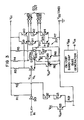
- the ECL gate is a base differential gate with an input transistor Q4 for receiving input signals of logic high and low potential levels at its base node, and a reference transistor element Q5. A threshold signal voltage level between the logic high and low potential input signal levels is applied at the base node of the reference transistor element Q5.
- the emitter terminals of ECL gate transistors Q4 and Q5 are coupled together at a common emitter node coupling.
- a current sink provided by emitter follower current source transistor element Q6 and emitter or tail resistor R6 is coupled between the common emitter node coupling of ECL gate transistors Q4 and Q5 and the low potential power rail V EE .
- the invention provides a translator circuit having at least one current sink with a first current source transistor element, first tail resistor element, and a temperature compensated current source voltage supply however derived, which supplies a temperature compensated current source voltage level V CS , referenced to the low potential power rail V EE .
- the temperature compensated current source voltage level V CS is supplied at the base node of the first current source transistor element.
- the components of the threshold clamp circuit are selected so that the threshold signal voltage level V TH is substantially centered between the logic high and low signal potential levels V IH ,V IL at the base node of the input transistor element.
- the voltage level shifting components of the threshold clamp circuit substantially cancel so that the temperature compensated current source voltage level V CS is applied substantially as the threshold voltage level V TH at the base node of the reference transistor element.
- the bias generator may be programed to deliver a V CS with slightly positive temperature coefficient to further compensate for the negative temperature coefficients of translator circuit V BE 's.
- the threshold clamp circuit 20 and base node of reference transistor element Q5 are coupled through current sourcing resistor element R5 to the high potential power rail V CC .
- Current sourcing resistor element R5 is a large resistor, in the order of for example 20K ohms relative to the tail resistor R51, for example in the order of 2K ohms.
- the tail resistor R51 is a relatively small resistance for generating a relatively large tail current by emitter follower current source transistor element Q61 through the tail resistor element R61.
- the current I R5 through resistor element R5 and the diode stack of the reference clamp circuit 20 is relatively smaller for example by approximately a factor of 10 than the emitter current I Q61 from the emitter of the second current source transistor element Q61.
Landscapes
- Engineering & Computer Science (AREA)
- Computer Hardware Design (AREA)
- Physics & Mathematics (AREA)
- Computing Systems (AREA)
- General Engineering & Computer Science (AREA)
- Mathematical Physics (AREA)
- Logic Circuits (AREA)
Applications Claiming Priority (2)
| Application Number | Priority Date | Filing Date | Title |
|---|---|---|---|
| US07/395,259 US5013941A (en) | 1989-08-17 | 1989-08-17 | TTL to ECL/CML translator circuit |
| US395259 | 1995-02-28 |
Publications (2)
| Publication Number | Publication Date |
|---|---|
| EP0413228A2 true EP0413228A2 (de) | 1991-02-20 |
| EP0413228A3 EP0413228A3 (en) | 1991-12-27 |
Family
ID=23562305
Family Applications (1)
| Application Number | Title | Priority Date | Filing Date |
|---|---|---|---|
| EP19900115110 Withdrawn EP0413228A3 (en) | 1989-08-17 | 1990-08-07 | Ttl to ecl/cml translator circuit |
Country Status (4)
| Country | Link |
|---|---|
| US (1) | US5013941A (de) |
| EP (1) | EP0413228A3 (de) |
| JP (1) | JP2852971B2 (de) |
| KR (1) | KR910005575A (de) |
Cited By (3)
| Publication number | Priority date | Publication date | Assignee | Title |
|---|---|---|---|---|
| EP0794620A3 (de) * | 1992-09-28 | 1997-10-29 | Motorola Inc | Spannungsversorgungsabhängiger Eingangspuffer |
| CN110299908A (zh) * | 2019-07-02 | 2019-10-01 | 浙江大华技术股份有限公司 | 一种电平转换电路 |
| CN115268555A (zh) * | 2022-07-27 | 2022-11-01 | 成都振芯科技股份有限公司 | 一种二阶温度补偿带隙基准电压电路及差分电路 |
Families Citing this family (10)
| Publication number | Priority date | Publication date | Assignee | Title |
|---|---|---|---|---|
| US5280200A (en) * | 1989-04-10 | 1994-01-18 | Tarng Min M | Pipelined buffer for analog signal and power supply |
| EP0417335A1 (de) * | 1989-09-11 | 1991-03-20 | Siemens Aktiengesellschaft | Schaltungsanordnung zur Wandlung von Signalen mit TTL-Pegel in Signale mit CML-Pegel oder ECL-Pegel |
| US5072136A (en) * | 1990-04-16 | 1991-12-10 | Advanced Micro Devices, Inc. | Ecl output buffer circuit with improved compensation |
| DE4236430C1 (de) * | 1992-10-28 | 1994-02-17 | Siemens Ag | Schaltstufe in Stromschaltertechnik |
| US5349253A (en) * | 1992-12-17 | 1994-09-20 | Vtc Inc. | Logic translator interfacing between five-volt TTL/CMOS and three-volt CML |
| DE69417622T2 (de) * | 1993-04-30 | 1999-09-09 | Stmicroelectronics | Spannungskomparator mit einer Summierung von auf dem Bandgap-Prinzip beruhenden Gleichströmen und diesen enthaltender Versorgungsspannungsschalter |
| US5432466A (en) * | 1994-03-31 | 1995-07-11 | Motorola, Inc. | ECL to TTL translator with power supply noise suppression |
| DE19624676C1 (de) * | 1996-06-20 | 1997-10-02 | Siemens Ag | Schaltungsanordnung zur Erzeugung eines Referenzpotentials |
| US6126258A (en) * | 1999-02-12 | 2000-10-03 | Agilent Technologies | System and method for interfacing signals with a processing element |
| KR100484257B1 (ko) * | 2002-09-12 | 2005-04-22 | 주식회사 하이닉스반도체 | 반도체 소자의 차동증폭형 입력 버퍼 |
Family Cites Families (12)
| Publication number | Priority date | Publication date | Assignee | Title |
|---|---|---|---|---|
| JPS4818671B1 (de) * | 1969-06-06 | 1973-06-07 | ||
| US3806736A (en) * | 1971-08-05 | 1974-04-23 | Siemens Ag | Temperature compensated emitter coupled logic circuit |
| US3946246A (en) * | 1974-09-03 | 1976-03-23 | Motorola, Inc. | Fully compensated emitter coupled logic gate |
| JPS5553924A (en) * | 1978-10-17 | 1980-04-19 | Hitachi Ltd | Semiconductor logic circuit |
| DE3217237A1 (de) * | 1982-05-07 | 1983-11-10 | Siemens AG, 1000 Berlin und 8000 München | Schaltungsanordnung zur pegelumsetzung |
| US4533842A (en) * | 1983-12-01 | 1985-08-06 | Advanced Micro Devices, Inc. | Temperature compensated TTL to ECL translator |
| JPS60174527A (ja) * | 1984-02-21 | 1985-09-07 | Nec Corp | 論理回路 |
| US4745304A (en) * | 1985-05-03 | 1988-05-17 | Advanced Micro Devices, Inc. | Temperature compensation for ECL circuits |
| US4654549A (en) * | 1985-06-04 | 1987-03-31 | Fairchild Semiconductor Corporation | Transistor-transistor logic to emitter coupled logic translator |
| US4736125A (en) * | 1986-08-28 | 1988-04-05 | Applied Micro Circuits Corporation | Unbuffered TTL-to-ECL translator with temperature-compensated threshold voltage obtained from a constant-current reference voltage |
| US4771191A (en) * | 1987-02-03 | 1988-09-13 | Julio Estrada | TTL to ECL translator |
| US4806800A (en) * | 1987-11-20 | 1989-02-21 | Tandem Computers Incorporated | TTL-to-ECL input translator/driver circuit |
-
1989
- 1989-08-17 US US07/395,259 patent/US5013941A/en not_active Expired - Lifetime
-
1990
- 1990-08-07 EP EP19900115110 patent/EP0413228A3/en not_active Withdrawn
- 1990-08-16 KR KR1019900012581A patent/KR910005575A/ko not_active Withdrawn
- 1990-08-17 JP JP2215933A patent/JP2852971B2/ja not_active Expired - Fee Related
Cited By (5)
| Publication number | Priority date | Publication date | Assignee | Title |
|---|---|---|---|---|
| EP0794620A3 (de) * | 1992-09-28 | 1997-10-29 | Motorola Inc | Spannungsversorgungsabhängiger Eingangspuffer |
| CN110299908A (zh) * | 2019-07-02 | 2019-10-01 | 浙江大华技术股份有限公司 | 一种电平转换电路 |
| CN110299908B (zh) * | 2019-07-02 | 2023-03-31 | 浙江大华技术股份有限公司 | 一种电平转换电路 |
| CN115268555A (zh) * | 2022-07-27 | 2022-11-01 | 成都振芯科技股份有限公司 | 一种二阶温度补偿带隙基准电压电路及差分电路 |
| CN115268555B (zh) * | 2022-07-27 | 2024-05-28 | 成都振芯科技股份有限公司 | 一种二阶温度补偿带隙基准电压电路及差分电路 |
Also Published As
| Publication number | Publication date |
|---|---|
| JP2852971B2 (ja) | 1999-02-03 |
| JPH03157014A (ja) | 1991-07-05 |
| EP0413228A3 (en) | 1991-12-27 |
| US5013941A (en) | 1991-05-07 |
| KR910005575A (ko) | 1991-03-30 |
Similar Documents
| Publication | Publication Date | Title |
|---|---|---|
| US6229353B1 (en) | Source-coupled logic with reference controlled inputs | |
| EP0305098B1 (de) | CMOS/ECL Konverter-Ausgangspufferschaltung | |
| KR100290966B1 (ko) | 신호의 스윙을 저감하는 cmos회로 | |
| US5013941A (en) | TTL to ECL/CML translator circuit | |
| WO1985002507A1 (en) | Temperature compensated ttl to ecl translator | |
| US5021691A (en) | Level conversion circuit having capability of supplying output signal with controlled logical level | |
| US7248079B2 (en) | Differential buffer circuit with reduced output common mode variation | |
| US6018261A (en) | Method and apparatus for providing a low voltage level shift | |
| US5001362A (en) | BiCMOS reference network | |
| US5045773A (en) | Current source circuit with constant output | |
| CA1194147A (en) | Signal translator with supply voltage compensation | |
| US4602207A (en) | Temperature and power supply stable current source | |
| US4684880A (en) | Reference current generator circuit | |
| US6642777B2 (en) | Voltage reference circuit with increased intrinsic accuracy | |
| US6255857B1 (en) | Signal level shifting circuits | |
| US5627456A (en) | All FET fully integrated current reference circuit | |
| US4970413A (en) | VBB-feedback threshold compensation | |
| US5774014A (en) | Integrated buffer circuit which functions independently of fluctuations on the supply voltage | |
| US5162676A (en) | Circuit having level converting circuit for converting logic level | |
| US5101125A (en) | Semiconductor integrated circuit with improved i/o structure with ecl to cmos to ecl conversion | |
| US5172015A (en) | Integratable transistor circuit for outputting logical levels | |
| US5028820A (en) | Series terminated ECL buffer circuit and method with an optimized temperature compensated output voltage swing | |
| JPH02101812A (ja) | 加速切換入力回路 | |
| KR100420689B1 (ko) | 버퍼회로 | |
| JPH04306017A (ja) | 参照電位発生回路 |
Legal Events
| Date | Code | Title | Description |
|---|---|---|---|
| PUAI | Public reference made under article 153(3) epc to a published international application that has entered the european phase |
Free format text: ORIGINAL CODE: 0009012 |
|
| AK | Designated contracting states |
Kind code of ref document: A2 Designated state(s): DE FR GB IT NL |
|
| PUAL | Search report despatched |
Free format text: ORIGINAL CODE: 0009013 |
|
| AK | Designated contracting states |
Kind code of ref document: A3 Designated state(s): DE FR GB IT NL |
|
| 17P | Request for examination filed |
Effective date: 19920509 |
|
| 17Q | First examination report despatched |
Effective date: 19950314 |
|
| STAA | Information on the status of an ep patent application or granted ep patent |
Free format text: STATUS: THE APPLICATION IS DEEMED TO BE WITHDRAWN |
|
| 18D | Application deemed to be withdrawn |
Effective date: 19950725 |