EP0414357A2 - Tastaturschnittstelle - Google Patents
Tastaturschnittstelle Download PDFInfo
- Publication number
- EP0414357A2 EP0414357A2 EP90307315A EP90307315A EP0414357A2 EP 0414357 A2 EP0414357 A2 EP 0414357A2 EP 90307315 A EP90307315 A EP 90307315A EP 90307315 A EP90307315 A EP 90307315A EP 0414357 A2 EP0414357 A2 EP 0414357A2
- Authority
- EP
- European Patent Office
- Prior art keywords
- data
- interface
- lines
- keyboard interface
- system interface
- Prior art date
- Legal status (The legal status is an assumption and is not a legal conclusion. Google has not performed a legal analysis and makes no representation as to the accuracy of the status listed.)
- Withdrawn
Links
Images


Classifications
-
- G—PHYSICS
- G06—COMPUTING OR CALCULATING; COUNTING
- G06F—ELECTRIC DIGITAL DATA PROCESSING
- G06F3/00—Input arrangements for transferring data to be processed into a form capable of being handled by the computer; Output arrangements for transferring data from processing unit to output unit, e.g. interface arrangements
- G06F3/01—Input arrangements or combined input and output arrangements for interaction between user and computer
- G06F3/02—Input arrangements using manually operated switches, e.g. using keyboards or dials
- G06F3/023—Arrangements for converting discrete items of information into a coded form, e.g. arrangements for interpreting keyboard generated codes as alphanumeric codes, operand codes or instruction codes
Definitions
- This invention relates in general to keyboard interfaces and in particular to a keyboard interface with an improved sytem for sensing and controlling the communication of data between the keyboard interface and a system interface.
- the input of data to a central processing system is by punching keys on a keyboard.
- the keyboard is normally equipped with a keyboard interface containing control logic for controlling the input information from the keys.
- the keyboard interface communicates with the system interface through a data line and a clock line. The communication between the two interfaces is controlled by both interfaces.
- the system interface will need to communicate to the keyboard interface its status, such as interrupt signals to indicate that it is not yet ready to receive data.
- the system interface communicates its status by means of status signals to the keyboard interface through the same clock and data lines.
- the status signals from the system interface are sensed through a sense clock line connected to the clock line and a sense data line connected to the data line.
- the data and clock lines also include gates to prevent the status signals from the system interface from otherwise affecting the keyboard interface.
- This invention is based on the recognition that the keyboard interface control system can be simplified by employing two input/output ports for connecting the keyboard interface with the clock line and the data line. Clock signals and data may be conveyed between the two interfaces through the clock and data lines and the two ports. In addition, status signals such as interrupt signals from the system interface on the clock and data lines may also be sensed through the two input/output ports.
- the keyboard interface control system of this invention therefore is simpler since no separate sense clock line or sense data line is required. As compared to the conventional design, the two gates required in conventional design can simply be eliminated.
- the keyboard interface apparatus of this invention comprises a keyboard interface having a first and a second input/output port, a clock line connecting the first port to a system interface and a data line connecting the second port to the system interface.
- the keyboard interface senses the two lines through the two ports for detecting status signals from the system interface through the two lines and the two input/output ports.
- the keyboard interface senses the two lines through the two ports and controls transmission and reception of data from the system interface through the data line and the second port.
- the method of transmission in this invention is applicable to a keyboard interface control system of the type described above in the summary of the invention.
- the system interface communicates interrupt signals to the keyboard interface by affecting the logic levels of the clock and data lines.
- the method comprises transmitting data to a system interface through the data line wherein the transmitting step comprises applying predetermined sequences of logic levels to the two lines.
- the logic levels of the two lines are then sensed by the keyboard interface to detect any interrupt signals from the system interface where the interrupt signals affect the logic levels of the two lines.
- the transmission of data is terminated.
- interrupt signals are detected by sensing whether the logic level of at least one of the two lines is different from those set by the keyboard interface.
- Another aspect of the invention is directed towards a method for controlling the reception of data by a keyboard apparatus from a system interface
- the keyboard apparatus includes a keyboard interface, a clock line and a data line connecting the two interfaces.
- the system interface transmits a parity bit in addition to data bits to the keyboard interface.
- the method comprises setting the clock and data lines to predetermined logic levels and sensing status signals from the system interface. When the status signal indicates data reception, the keyboard interface then receives data from the system interface through the data line.
- the method also comprises parity checking the data received to determine the accuracy of reception.
- Fig. 1 is a functional block diagram of a keyboard interface, a system interface, clock and data lines, a sense clock line and a sense data line to illustrate a conventional keyboard interface control system.
- the keyboard interface control system 1 transmits data to a system interface 4 through a data line 17 assisted by clock signals also sent by system 1 to system interface 4 through a clock line 16.
- the keyboard interface system 1 includes a keyboard interface 3, a sense clock line 13 and a sense data line 15 and two gates 10, 11.
- the system interface communicates its status by means of status signals to the keyboard interface through the clock and data lines 16, 17, sense clsock and data lines 13, 15 and input ports 13a, 15a.
- the two gates 10, 11 are buffers used to prevent any status signals from the system interface 4 on lines 16, 17 from affecting the output ports 12a, 14a of the keyboard interface.
- clock signals are transmitted through line 12, gate 10 and line 16 to system interface 4 to assist the transmission of data sent at the same time through line 14, gate 11 and line 17.
- the status signals from system interface 4 are sensed through lines 13, 15 and input ports 13a, 15a by the keyboard interface 3.
- the clock signals and data signals are sent through output ports 12a, 14a.
- the conventional system of Fig. 1 requires separate input and output ports, separate sensing lines 13, 15 and buffer gates 10, 11.
- the keyboard interface system 2 includes a keyboard interface 5 with two input/output ports 21, 22 for transmitting clock signals and data signals through lines 16, 17 as well as sensing the status signals from the system interface 4 present on these two lines.
- System 2 is therefore simpler than system 1 of Fig. 1. This reduces the complexity of the system and permits system 2 to be made on a single chip.
- the system of Fig. 2 is suitable for the transmission of serial data between the two interfaces.
- System 2 or interface 5 includes a microprocessor (not shown in Fig. 2).
- the input/output 21, 22 are for transmitting clock and data signals to and receiving same from system interface 4 as well as for sensing the status signals from system interface 4 through lines 16, 17.
- Keyboard interface 5 will interpret the status signals sent from system interface 4 before and during the data transmission and reception processes between the two interfaces. Before the keyboard interface starts transmitting the data to the system interface, it checks the presence of any status signals from the system interface. Since the clock and data lines are used for data transmission as well as for the transmission of status signals, the keyboard interface will need to distinguish between signals on the two lines used for data transmission and status signals from the system interface on the same two lines. It does so by applying predetermined logic signals to the clock and data lines for the purpose of data transmission and then detecting whether the logic levels of the two lines are different from those set by the keyboard interface. The keyboard interface initiates data transmission by sending a start bit indicating that the bits that follow are data bits.
- the keyboard interface pulls both clock and data lines high and then detects whether the clock line or the data line or both have been pulled low by the system interface to indicate an interrupt. If either or both lines have been pulled low, the keyboard interface aborts the transmission process. After the start bit has been transmitted, the keyboard interface detects only whether the clock line (but not the data line) has been pulled low when the keyboard interface has set the clock line to high, in order to detect status signals from the system interface.
- the keyboard interface pulls both the clock and data lines high.
- this represents the status signal from the system interface that the keyboard interface 5 should stop sending data and should be prepared to receive data.
- system interface 4 pulls the clock line 16 high and the data line 17 low, this represents the status signal from the system interface that the keyboard interface should start receiving data from the system interface.
- clock line 16 is pulled low and data line 17 is pulled high by the system interface, this represents the status signal that the keyboard interface should stop transmitting data.
- the clock and data lines 16, 17 are both pulled high by the system interface, this represents the status that the keyboard interface 5 is permitted to transmit data to the system interface 4.
- the four status signals from the system interface are illustrated in the table below.
- CLOCK DATA FUNCTION Low High System inhibit keyboard (KB) Don't care Low System wants to send data to KB Low first Low System wants to send data to KB High High KB may transmit to system
- the keyboard interface 5 Before the initiation of data transmission, the keyboard interface 5 first pulls clock line 16 and data line 17 high and then senses the logic levels of the two lines. The logic levels of the two lines sensed then indicate one of four possible status signals from system interface 4.
- the clock and data lines are also used for the communication of digital data between the two interfaces.
- a microprocessor (not shown in Fig. 2) in interface 5 controls the communication of data on the two lines, where level trigger is employed.
- the keyboard interface 5 will load data onto data line 17 only when the clock signal is previously at the high logic level (i.e. high, e.g. at time t5 in Fig. 6).
- Interface 5 will accept data from line 17 only when the clock line is at the high logic level (i.e. high, e.g. at time t5 in Fig. 7).
- the serial communication of data between interfaces 4, 5 is illustrated by the communication of 11 bits, including a start bit code, eight data bits (bit 0-bit 7), a parity check bit code and a stop bit code.
- the start bit code is represented by the low logic level and the stop bit code by the high logic level.
- odd parity check is employed. In other words, when the number of ones added to the value of a parity check bit is odd, that means the data has been transmitted without error.
- Figs. 3A, 3B are flow charts illustrating the steps by which the keyboard interface transmits data to the system interface. Unless specified otherwise, the steps described are those taken by the keyboard interface.
- First the clock line 16 and data line 17 are pulled to the high logic level (block 50), as shown at time t1 in Fig. 6.
- Data line 17 is sensed through port 22 (diamond 52). If the data line is low, the keyboard interface executes a sub-routine 54 which is set forth in more detail in Fig. 4. If the data line remains high, the keyboard interface further checks to see if the clock line is low (diamond 56). If the clock line is low, the keyboard interface also executes sub-routine 54 of Fig, 4.
- Steps 50 through 56 are executed before any data is transmitted.
- the keyboard interface is ready to transmit any data, it pulls both lines high and detects whether either one or both lines have been pulled low by the system interface. If either or both lines have been pulled low by the system interface for a predetermined time period the transmission process is terminated.
- the subroutine for checking whether either or both lines have been pulled low by the system interface to indicate an interrupt signal will be explained in more detail below in reference to Fig. 4.
- the transmission process continues and the keyboard interface pulls the data line low (block 58) at time t2 illustrated in Fig. 6. Even at this point, the keyboard interface continues to check and see if the clock line has been pulled low by the system interface (diamond 60). If it has, the keyboard interface exits to marker 3 at which point the keyboard interface stores the data to be transmitted in a buffer (not shown) and processes the interrupt signal from the system interface as illustrated in Fig. 3B. If the clock line has not been pulled low, the keyboard interface prepares eight bits of data to be transmitted (block 62). The keyboard interface then pulls the clock line low at time t3 illustrated in Fig. 6.
- the start bit is indicated when both lines 16, 17 are pulled low, such as between times t3 and t4.
- the clock line is then pulled high at time t4 as shown in Fig. 6 after a predetermined delay according to a square wave clock signal.
- a square wave clock signal with a predetermined frequency is applied to the clock line 16.
- clock line 16 After clock line 16 has been pulled high, the clock line is sensed to see if it is low (diamond 70). It if is, the keyboard interface moves to marker 3 to store prepared data in a buffer and process the interrupt signal (block 61).
- the keyboard interface checks the value of the 1st bit (bit 0). If the value of the bit is a "0" (block 72), the data line is pulled low; if the value of the bit is a "1", the data line is pulled high (blocks 74, 76) to supply the 1st bit to data line 17. Then the next bit is prepared and the clock line is checked to see if it is still at logic low (block 78, diamond 80). If the clock line is low, the keyboard interface moves to marker 3 to store the data in the buffer and to process the interrupt signal. If the clock line is high, the clock line is pulled low (block 82) at time t5 illustrated in Fig. 6.
- the interface then checks to see if all eight bits have been sent (diamond 84). If not all eight bits have been sent, the interface moves to marker 2 to reenter the main program between blocks 66, 68 to send more data and to detect interrupt signals from the system interface as discussed above. If all eight bits have been sent, the clock line is pulled high (block 86) at time t6 as illustrated in Fig. 6. The parity and stop bits are then sent (block 88). After all 11 bits have been transmitted, the transmission process is concluded. Obviously, a different number as well as different type of bits arranged in a different manner may be transmitted by the keyboard interface using essentially the same method and apparatus as that described; all such variations are within the scope of the invention.
- the clock signals on clock line 16 causes the data bits to be strobed and loaded onto data line 17.
- the status of only the clock line is sensed to determine whether the logic level of the line differs from what it should be as controlled by the keyboard interface. If any difference is detected, this is interpreted as an interrupt signal from the system interface.
- the data prepared to be transmitted is stored in a buffer and the keyboard interface processes the interrupt signal to abort the transmission process.
- Fig. 4 is a flow chart illustrating in more detail the sub-routine 54 of Fig. 3A.
- the microprocessor (not shown in Fig. 2) of the keyboard interface includes a counter. First a constant is stored in the counter (block 102). Then the logic level of the clock line is sensed (diamond 104). If the clock line is not low, the logic level of the data line is sensed (block 106, diamond 108). If the data line is also high, this means that no interrupt signal has been received from the system interface. In such event, the keyboard interface returns to the main program and block 58 of Fig. 3A. If either the clock line or the data line is still low as detected in diamonds 104, 108, the counter is decremented by one (block 110).
- the reading of the counter is checked to see if it is 0 (diamond 112). If the counter reads 0, the keyboard interface thereby terminates the transmission process. If the counter is still not 0, the keyboard interface returns to diamond 104 to recheck the clock and data lines. In other words, after the keyboard interface pulls both the clock and data lines high at time t1 in block 50, the keyboard interface checks the logic levels of the two lines for a time period which is a function of the constant stored in the counter. If, at the expiration of such time period, either one or both clock and data lines are still low, the keyboard interface interprets this as an interrupt signal from the system interface and therefore aborts the transmission process before any data is transmitted.
- the purpose of the subroutine in Fig. 4 is to ensure that the low logic levels on the clock or data lines are indeed caused by the system interface, thereby indicating an interrupt, and not by extraneous factors such as noise.
- Marker 3 in the flow chart of Figs. 3A, 3B is for storing the prepared data in the keyboard interface in a buffer in a microprocessor (not shown in Fig. 2) for temporary storage.
- the keyboard interface continues to sense the logic level of the clock line. When the interrupt signal is no longer detected, the keyboard interface resumes the transmission process. To send an interrupt signal to stop the keyboard interface from transmitting data, the system interface forces the clock line 16 or data line 17 low.
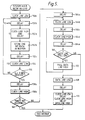
- Fig. 5 is a flow chart illustrating the steps by which the keyboard interface receives data from the system interface. It is to be interpreted together with the timing diagram of Fig. 7.
- the steps taken by the keyboard interface 5 are illustrated by solid lines and the steps taken by the system interface 4 are illustrated by dotted lines.
- the keyboard interface Upon initiation and before it is determined whether the keyboard interface should transmit or receive data, the keyboard interface always pulls the clock line and data line high (not shown in Fig. 5), such that the logic levels of the two lines before time t1 are as illustrated in Fig. 7. But if the system interface 4 pulls the clock line 16 low for a time period, such as illustrated by the dotted line beginning at time t1, this means that the keyboard interface 5 should stop sending data and/or it should be prepared to receive data.
- this signal causes the keyboard interface to stop all functions or processes except to start receiving data.
- the system interface pulls the clock line low at time t1, it pulls the clock line high again; the low logic level of the data line and high logic level of the clock line convey a start bit code to the keyboard interface.
- the keyboard interface then applies a square-shaped clock signal to the clock line and pulls the clock line low at time t3 and pulls it high again at time t4 as shown in Fig. 7 (blocks 150a, 150b).
- the keyboard interface is ready to receive data from the data line 17 when the clock line is at a high logic level.
- a time t5 the keyboard interface 5 receives and stores in a buffer (not shown in Fig. 2) one bit of data from the system interface through data line 17 (blocks 152a-152c). At time t51, clock line is pulled low (block 154).
- M bits of data are transmitted by the system interface to the keyboard interface where M is 8 and the data transmitted is 11101110.
- the above steps are illustrated in blocks 150-154.
- the keyboard interface then checks to see if all 8 bits have been received (diamond 156). If they have not been, the keyboard interface returns to block 150b.
- the bits of data are stored in a buffer (not shown in Fig. 2) as illustrated in block 152b. If all 8 bits have been received, the keyboard interface will apply a cycle of low and high logic levels such as at times t6 and t7 in Fig. 7 (blocks 158a, 158b). When a clock line has been pulled high at time t7, the keyboard interface receives a parity bit from line 17.
- the microprocessor (now shown in Fig. 2) in the keyboard interface adds the number of 1's stored in the buffer to the parity bit to see if the result is odd. If the result is even, this indicates that the data received is incorrect so that the 8 bits of data received will be discarded from the buffer. The process of receiving data is thereby terminated. At that point, the keyboard interface may notify the system interface to retransmit data, such as by repeating the above described steps beginning at block 150a.
- line 16 is pulled low and high after delays such as at times t9 and t10 in Fig. 7 (blocks 164a-164e) whereupon the keyboard interface senses whether the data line is low (diamond 166).
- the data line at the logic high level indicates the stop bit code. Interference and noise from the environment may affect the logic level of data line 17 at this time. For this reason, the logic level of line 17 is sensed continuously to determine whether it remains at a steady high logic level as illustrated in the loop consisting of blocks 164a-164e, diamond 166 and block 172, block 172 being described below.
- the stop bit code is recorded and line 17 is pulled low first and then line 16 is pulled low such as at time t11 in Fig. 7 (blocks 168, 170).
- the two lines are again pulled high after a time period (block 170) to indicate the end of receiving data. With both lines high, the keyboard interface is ready to perform the next cycle of data transmission or reception. If the data line is low (diamond 166), it is pulled high (block 172) and the keyboard interface returns to block 164b until the data line remains at a high level.
Landscapes
- Engineering & Computer Science (AREA)
- General Engineering & Computer Science (AREA)
- Theoretical Computer Science (AREA)
- Human Computer Interaction (AREA)
- Physics & Mathematics (AREA)
- General Physics & Mathematics (AREA)
- Input From Keyboards Or The Like (AREA)
- Communication Control (AREA)
Applications Claiming Priority (2)
| Application Number | Priority Date | Filing Date | Title |
|---|---|---|---|
| US397000 | 1989-08-22 | ||
| US07/397,000 US5146567A (en) | 1989-08-22 | 1989-08-22 | Keyboard interface |
Publications (2)
| Publication Number | Publication Date |
|---|---|
| EP0414357A2 true EP0414357A2 (de) | 1991-02-27 |
| EP0414357A3 EP0414357A3 (en) | 1992-06-24 |
Family
ID=23569483
Family Applications (1)
| Application Number | Title | Priority Date | Filing Date |
|---|---|---|---|
| EP19900307315 Withdrawn EP0414357A3 (en) | 1989-08-22 | 1990-07-04 | Keyboard interface |
Country Status (2)
| Country | Link |
|---|---|
| US (1) | US5146567A (de) |
| EP (1) | EP0414357A3 (de) |
Families Citing this family (9)
| Publication number | Priority date | Publication date | Assignee | Title |
|---|---|---|---|---|
| US5524237A (en) * | 1992-12-08 | 1996-06-04 | Zenith Electronics Corporation | Controlling data transfer between two microprocessors by receiving input signals to cease its data output and detect incoming data for reception and outputting data thereafter |
| US5758098A (en) * | 1994-05-12 | 1998-05-26 | Apple Computer, Inc. | Method and apparatus for providing a high throughput two-conductor serial interface with support for slave device detection |
| US6091783A (en) * | 1997-04-25 | 2000-07-18 | International Business Machines Corporation | High speed digital data transmission by separately clocking and recombining interleaved data subgroups |
| EP1128271A1 (de) * | 2000-02-22 | 2001-08-29 | THOMSON multimedia S.A. | Verfahren zur seriellen Datenübertragung zwischen zwei elektronischen Busstationen und Busstation zur Verwendung in demselben Verfahren |
| US7089338B1 (en) * | 2002-07-17 | 2006-08-08 | Cypress Semiconductor Corp. | Method and apparatus for interrupt signaling in a communication network |
| US7310498B2 (en) * | 2003-04-09 | 2007-12-18 | Standard Microsystems Corporation | Communication protocol for personal computer system human interface devices over a low bandwidth, bi-directional radio frequency link |
| US20040203480A1 (en) * | 2003-04-09 | 2004-10-14 | Dutton Drew J. | Configuration and management of human interface and other attached devices through bi-directional radio frequency link |
| US20080005262A1 (en) * | 2006-06-16 | 2008-01-03 | Henry Wurzburg | Peripheral Sharing USB Hub for a Wireless Host |
| US9959223B2 (en) * | 2013-05-08 | 2018-05-01 | Nxp B.V. | Method and system for interrupt signaling in an inter-integrated circuit (I2C) bus system |
Family Cites Families (12)
| Publication number | Priority date | Publication date | Assignee | Title |
|---|---|---|---|---|
| US3872446A (en) * | 1971-05-14 | 1975-03-18 | Raytheon Co | Visual display system |
| US3774161A (en) * | 1971-05-14 | 1973-11-20 | Raytheon Co | Visual display system |
| JPS55129826A (en) * | 1979-03-28 | 1980-10-08 | Canon Inc | Input unit |
| US4513390A (en) * | 1979-06-08 | 1985-04-23 | Planning Research Corporation | System for digital transmission and synthesis of integrated data |
| US4527250A (en) * | 1980-09-11 | 1985-07-02 | Allen-Bradley Company | Video computer terminal with detachable intelligent keyboard module |
| JPS57105023A (en) * | 1980-12-23 | 1982-06-30 | Toshiba Corp | Data transfer system |
| US4460957A (en) * | 1981-08-12 | 1984-07-17 | International Business Machines Corporation | Self-pacing serial keyboard interface for data processing system |
| JPS59123336A (ja) * | 1982-12-28 | 1984-07-17 | インタ−ナシヨナル ビジネス マシ−ンズ コ−ポレ−シヨン | 直列キ−ボ−ド・インタフエ−ス・システム |
| JPS63118856A (ja) * | 1986-11-06 | 1988-05-23 | Nec Corp | シリアル・バス・インタフエ−ス回路 |
| US4814712A (en) * | 1987-06-17 | 1989-03-21 | General Electric Company | Test kit for a circuit breaker containing an electronic trip unit |
| US5146584A (en) * | 1989-02-27 | 1992-09-08 | Data General Corporation | Keyboard interface system allowing a synchronous keyboard to communicate with a host processor asynchronously by manipulating the keyboard clock's state |
| US5056057A (en) * | 1989-05-03 | 1991-10-08 | Compaq Computer Corporation | Keyboard interface for use in computers incorporating terminate-and-stay-resident programs |
-
1989
- 1989-08-22 US US07/397,000 patent/US5146567A/en not_active Expired - Lifetime
-
1990
- 1990-07-04 EP EP19900307315 patent/EP0414357A3/en not_active Withdrawn
Also Published As
| Publication number | Publication date |
|---|---|
| US5146567A (en) | 1992-09-08 |
| EP0414357A3 (en) | 1992-06-24 |
Similar Documents
| Publication | Publication Date | Title |
|---|---|---|
| US5247163A (en) | IC card having a monitor timer and a reset signal discrimination circuit | |
| US4984190A (en) | Serial data transfer system | |
| EP0335424B1 (de) | Paritätsprüfgerät | |
| EP0414357A2 (de) | Tastaturschnittstelle | |
| US5889817A (en) | Communication system with data comparison circuit | |
| EP0287678B1 (de) | Datenübertragungssystem mit übertragunsdiskriminierungsschaltung | |
| US8172150B2 (en) | Integrated circuit card | |
| KR0131601B1 (ko) | 키보드 인터페이스 | |
| EP0308510A4 (de) | Schnittstellenverfahren in numerischer steuerungsvorrichtung. | |
| JPH03134721A (ja) | キーボードインタフェース | |
| JP3305667B2 (ja) | ファームウェアデータの書込み方法 | |
| JP2523874B2 (ja) | 非同期式シリアルデ―タ伝送装置 | |
| US5303345A (en) | Method for controlling data sending and receiving operations of a microprocessor | |
| JP2001005922A (ja) | 非接触icカードリーダ装置 | |
| JPH0561988A (ja) | 識別システム | |
| JP2830380B2 (ja) | 識別システム及び物品識別方法 | |
| JP2945123B2 (ja) | 通信システム | |
| JP2534295B2 (ja) | 非接触icカ―ドの識別方法 | |
| JP2843449B2 (ja) | データ転送装置 | |
| JP2898025B2 (ja) | 入出力ターミナル | |
| KR19980073172A (ko) | 비동기식 데이터 송수신 장치의 에러 검출 방법 | |
| JPS63284954A (ja) | ブレ−クレベル検出回路 | |
| JPH01116747A (ja) | キャッシュlsi | |
| JPH03192939A (ja) | 送受信方法 | |
| JPH06284121A (ja) | 同期ワード検出方式 |
Legal Events
| Date | Code | Title | Description |
|---|---|---|---|
| PUAI | Public reference made under article 153(3) epc to a published international application that has entered the european phase |
Free format text: ORIGINAL CODE: 0009012 |
|
| AK | Designated contracting states |
Kind code of ref document: A2 Designated state(s): DE FR GB IT |
|
| PUAL | Search report despatched |
Free format text: ORIGINAL CODE: 0009013 |
|
| AK | Designated contracting states |
Kind code of ref document: A3 Designated state(s): DE FR GB IT |
|
| 17P | Request for examination filed |
Effective date: 19921224 |
|
| STAA | Information on the status of an ep patent application or granted ep patent |
Free format text: STATUS: THE APPLICATION HAS BEEN WITHDRAWN |
|
| 18W | Application withdrawn |
Withdrawal date: 19950418 |