EP0414619B1 - Procédé de réglage de la réponse en fréquence d'un dispositif à filtrage du type à trois conducteurs - Google Patents
Procédé de réglage de la réponse en fréquence d'un dispositif à filtrage du type à trois conducteurs Download PDFInfo
- Publication number
- EP0414619B1 EP0414619B1 EP90420287A EP90420287A EP0414619B1 EP 0414619 B1 EP0414619 B1 EP 0414619B1 EP 90420287 A EP90420287 A EP 90420287A EP 90420287 A EP90420287 A EP 90420287A EP 0414619 B1 EP0414619 B1 EP 0414619B1
- Authority
- EP
- European Patent Office
- Prior art keywords
- conducting layer
- circuit end
- resonator
- open circuit
- filter device
- Prior art date
- Legal status (The legal status is an assumption and is not a legal conclusion. Google has not performed a legal analysis and makes no representation as to the accuracy of the status listed.)
- Expired - Lifetime
Links
- 239000004020 conductor Substances 0.000 title claims description 26
- 238000000034 method Methods 0.000 title claims description 12
- 239000000758 substrate Substances 0.000 claims description 57
- 238000005520 cutting process Methods 0.000 claims description 3
- 230000003247 decreasing effect Effects 0.000 claims description 3
- 238000003754 machining Methods 0.000 claims description 3
- 238000005488 sandblasting Methods 0.000 claims description 3
- 230000005540 biological transmission Effects 0.000 description 2
- 229910010293 ceramic material Inorganic materials 0.000 description 2
- 238000004519 manufacturing process Methods 0.000 description 2
- 230000002093 peripheral effect Effects 0.000 description 2
- 229910052761 rare earth metal Inorganic materials 0.000 description 2
- GWEVSGVZZGPLCZ-UHFFFAOYSA-N titanium dioxide Inorganic materials O=[Ti]=O GWEVSGVZZGPLCZ-UHFFFAOYSA-N 0.000 description 2
- 238000010276 construction Methods 0.000 description 1
- 238000007796 conventional method Methods 0.000 description 1
- 239000003989 dielectric material Substances 0.000 description 1
- 229910052751 metal Inorganic materials 0.000 description 1
- 239000002184 metal Substances 0.000 description 1
Images


Classifications
-
- H—ELECTRICITY
- H01—ELECTRIC ELEMENTS
- H01P—WAVEGUIDES; RESONATORS, LINES, OR OTHER DEVICES OF THE WAVEGUIDE TYPE
- H01P1/00—Auxiliary devices
- H01P1/20—Frequency-selective devices, e.g. filters
- H01P1/201—Filters for transverse electromagnetic waves
- H01P1/203—Strip line filters
- H01P1/20327—Electromagnetic interstage coupling
- H01P1/20336—Comb or interdigital filters
Definitions
- the present invention relates to a method of adjusting a frequency response in a filter device of three-conductor type which may be used as a band-pass filter for example.
- a filter device of three-conductor type which is utilized as a band-pass filter for a microwave range.
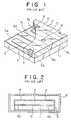
- An example of such a conventional filter device is illustrated in Figs. 1 and 2.
- Figs. 1 and 2 As will be seen in Figs. 1 and 2, it comprises a lower dielectric substrate 1 and an upper dielectric substrate 2 which are stacked to each other.
- Each of the dielectric substrates 1 and 2 may be of dielectric ceramic material having a high dielectric constant and a lower dielectric loss such as BaO-TiO 2 , BaO-TiO 2 -rare earth or the like.
- the lower dielectric substrate 1 is provided with an external ground conducting layer 3 on the peripheral portion and bottom surface thereof.
- the upper dielectric substrate 2 is provided with an external ground conducting layer 4 on the peripheral portion and upper surface thereof.
- On the upper surface of the lower dielectric substrate 1 are disposed a plurality of stripline resonator conducting layers 5, 6 and 7 which form a filter element.
- Each resonator conducting layer has one end or an open circuit end (5a, 6a and 7a) spaced from the ground conducting layer 3 and the other end or a short circuit end (5b, 6b and 7b) connected to the ground conducting layer 3.
- the open circuit ends 5a, 6a and 7a of the respective resonator conducting layers 5, 6 and 7 are alternately disposed so as to form an interdigitated configuration.
- the upper dielectric substrate 2 is fixed on the lower dielectric substrate 1, and the ground conducting layers 3 and 4 of the respective dielectric substrates are connected to each other.
- the filter device of this type has a frequency response which depends on the configuration and dielectric constant of the substrates, and the dimension of the resonator conductors.
- the dielectric constant of the substrates and the size of the resonator conducting layers are strictly determined. However, it can not be avoided that there may occur any dispertions in the dielectric constant of the substrates and in the dimension of the resonator conducting layers. It is, therefore, necessary to adjust the frequency response of the filter device after being completed.
- the adjustment of the frequency response can not be performed by adjusting the length of the resonator conducting layers because they are embedded in the dielectric substrates.
- One solution to this problem has been proposed in the above-mentioned document US-A-4157517.
- the frequency of the filter is previously set at a lower level than a desired one, and the external conductor or ground conducting layer 4 provided on the upper surface of the upper substrate 2 is partially removed at regions 8 adjacent the open circuit ends of the resonator conducting layers 5, 6 and 7 to reduce the capacitance between the external conducting layer 4 and the respective resonator conducting layers and to increase the response frequency of the filter thereby making it possible to adjust the frequency.
- Document WO-A-8500929 discloses a filter comprising a rectangular parallelepipedic block of dielectric material which is provided with a number of through holes to form resonators, each hole being extended from one end face to the other end face of the block. Since each of the resonators has an exposed open circuit end, partial removal of said exposed end can here be easily performed for adjusting the frequency of the filter. On the contrary, it is difficult to externally adjust the length of each resonator line in a filter device of the above-mentioned type, in which a plurality of stripline resonator conducting layers are embedded between a pair of dielectric substrates.
- Document JP-A-63219201 discloses a method for adjusting the frequency response of a stripline filter, by arranging a dielectric chip having an upper surface coated with a conductive material. However, this document does not teach that the open circuit end of each resonator layer, and the adjacent substrate portion, is previously removed.
- Another object of the invention is to provide a filter device of a three-conductor structure type which fully meets with the requirement for smaller and thinner dimension.
- the open circuit end of said each resonator conducting layer and the associated lateral surface of said each substrate may be partially removed by using a cutting tool, a laser beam machining, a sand blasting or the like.
- the filter device is constructed to have a resonant frequency lower than an intended frequency before adjusting thereof.
- each resonator conducting layer By partially removing the open circuit end of each resonator conducting layer and the associated lateral surface portion of said each substrate which corresponds to the open circuit end of each resonator conducting layer, the length of each resonator conducting layer is shortened and thus a resonant frequency is increased.
- the resonant frequency may be decreased depending on the quantity of the conductor member to be added.
- the removed open circuit end portion may be provided with an additional conductor member for decreasing a resonant frequency of the filter device.
- FIG. 3 there is shown a three-conductor type filter for which the present invention can be applied.
- the illustrated filter 10 comprises a lower and upper dielectric substrates 11 and 12 which are stacked to each other upon the assembling of the filter.
- Each of the dielectric substrates 11 and 12 may be of dielectric ceramic material having a high dielectric constant and a lower dielectric loss such as BaO-TiO 2 , BaO-TiO 2 -rare earth or the like.
- the lower dielectric substrate 11 is provided with a ground conducting layer 13 on the lower or outer surface thereof.
- the upper dielectric substrate 12 is provided with a ground conducting layer 14 on the upper or outer surface thereof.
- On the upper or inner surface of the lower dielectric substrate 11 are provided a plurality of stripline resonator conducting layers 15, 16 and 17 which form a filter element of an interdigital type.
- each resonator conducting layer has one end or an open circuit end (15a, 16a and 17a) extended to the edge of the lateral surface 18 of the each dielectric substrate and thus spaced from the ground conducting layers 13 and 14 on the outer surface of the respective dielectric substrates 11 and 12.
- each resonator conducting layer is extended across the lateral surface 18 of the lower dielectric substrate 11 and connected to the ground conducting layers 13 and 14 on the outer surface of the respective dielectric substrates 11 and 12.
- the open circuit ends 15a, 16a and 17a of the respective resonator conducting layers 15, 16 and 17 are alternately disposed so as to form an interdigital type resonator.
- the upper dielectric substrate 12 is fixed on the lower dielectric substrate 11, and the ground conducting layers 13 and 14 of the respective dielectric substrates are connected to each other through the short circuit ends 15b, 16b and 17b of the respective resonator conducting layers 15, 16 and 17.
- the resonator conducting layers 15 and 17 have lateral extensions 15c and 17c, respectively.
- One of the lateral extensions 15c and 17c is connected to a signal input terminal, not shown, and the other extension is connected to a signal output terminal, not shown.
- each of the respective resonator conducting layers 15, 16 and 17, and the lateral surface of each substrate are partially removed at each open circuit end portion and the region 19 of the lateral surface of each substrate which surrounds the open circuit end of each resonator conducting layer.
- This removing operation may be performed by means of a cutting tool, a laser beam machining, a sand blasting or the like. In this way, the filter can be tuned to a desired frequency response.
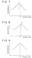
- the filter has a center frequency f 1 which is slightly lower than a desired response frequency f 0 before the frequency adjustment is made.
- the center frequency f 1 is shifted toward a higher frequency zone so that it becomes identical with the desired response frequency f 0 as shown in Fig. 9.
- the casing 20 may be metal, and has an inner height equal to the height of the filter and a width larger than that of the filter.
- Fig. 6 illustrates another embodiment of the present invention in which an additional adjusting means is provided for shifting the center frequency of the filter toward a lower frequency zone.
- each resonator conducting layer is lengthened, so that the center frequency f 2 is shifted toward a lower frequency zone so that it becomes identical with the desired response frequency f 0 as shown in Fig. 9.
- the upper dielectric substrate 12 may also be provided with a transmission line pattern of resonator conducting layers on the lower surface, which is disposed to have a reflected image relation with respect to the stripline pattern of the resonator conducting layers 15, 16 and 17 on the lower dielectric substrate 11.
- the stripline pattern on the lower dielectric substrate 11 comes into face-to-face contact with the transmission line pattern on the upper dielectric substrate 12 without occurring any gaps between the lower dielectric substrate 11 and the upper dielectric substrate 12.
- stripline pattern of the resonator conducting layers 15, 16 and 17 may be formed as a comb type in which the open circuit ends and the short circuit ends thereof are disposed at the same sides, respectively.
- the frequency adjusting of the filter is performed by partially removing the open circuit end of each resonator conductor and the regions of the lateral surfaces of each substrate surrounding each open circuit end, and at need by adding an compensating conductor member to the partially removed open circuit end portion of each resonator conductor. Therefore, since the outer conductor of the filter is not removed at regions which are to be abutted on the inner surface of a casing as in the case of the conventional filter device, the present invention has an advantage that there is no variation or deviation in the set frequency characteristic of the filter when the filter device is completed by inserting the filter into the casing. The present invention has also an advantage that a frequency adjustment can be correctly made without increasing the thickness or height of the casing.
Landscapes
- Physics & Mathematics (AREA)
- Electromagnetism (AREA)
- Control Of Motors That Do Not Use Commutators (AREA)
Claims (3)
- Procédé de réglage de la réponse en fréquence d'un dispositif de filtrage (10) du type à structure à trois conducteurs, comprenant deux substrats diélectriques (11,12) comportant chacun une surface extérieure pourvue d'une couche conductrice externe de mise à la terre (13,14) et des surfaces latérales opposées (18) dépourvues de couche conductrice de mise à la terre, et une pluralité de couches conductrices formant résonateur, en forme de bandes (15,16,17), qui sont insérées entre lesdits substrats diélectriques (11,12), chaque couche conductrice formant résonateur (15,16,17) possédant une extrémité en court-circuit (15b,16b,17b), raccordée à la couche conductrice de mise à la terre (13,14) sur la surface extérieure de chacun des substrats (11,12), ainsi qu'une extrémité en circuit ouvert (15a,16a,17a), tournée vers un bord de la surface latérale associée (18) de chacun des substrats (11,12), caractérisé en ce qu'il comprend l'opération consistant à enlever partiellement la matière de l'extrémité en circuit ouvert (15a,16a,17a) de chaque couche conductrice formant résonateur (15,16,17) et la surface latérale associée (18) de chaque substrat (11,12), dans une région (19) qui entoure l'extrémité en circuit ouvert (15a,16a,17a) de chaque couche conductrice formant résonateur (15,16,17), pour accorder le dispositif de filtrage (10) sur une réponse en fréquence désirée, et en ce qu'il comprend l'opération supplémentaire consistant à disposer un élément conducteur additionnel (21) sur l'extrémité en circuit ouvert (15a,16a,17a) de chaque couche conductrice formant résonateur (15,16,17), du côté de la surface latérale (18) de chacun desdits substrats (11,12), en vue de compenser tout dépassement du réglage effectué lors de l'opération d'enlèvement partiel de la matière de ladite extrémité en circuit ouvert (15a,16a,17a).
- Procédé selon la revendication 1, caractérisé en ce que ladite opération d'enlèvement de matière est réalisée en utilisant un outil de coupe, un usinage par faisceau laser, un sablage ou similaire.
- Dispositif de filtrage du type à structure à trois conducteurs, comprenant deux substrats diélectriques (11,12) comportant chacun des surfaces latérale et extérieure, une couche conductrice externe de mise à la terre (13,14) prévue sur la surface extérieure de chacun des substrats diélectriques (11,12), une pluralité de couches conductrices formant résonateur, en forme de bandes (15,16,17), qui sont insérées entre lesdits substrats diélectriques (11,12), chaque couche conductrice formant résonateur (15,16,17) possédant une extrémité en court-circuit (15b,16b,17b), raccordée à la couche conductrice de mise à la terre (13,14) sur la surface extérieure de chacun des substrats (11,12), et une extrémité en circuit ouvert (15a,16a,17a), tournée vers un bord d'une surface latérale (18) de chacun des substrats (11,12), caractérisé en ce que l'extrémité en circuit ouvert (15a,16a,17a) de chaque couche conductrice formant résonateur (15,16,17) possède une partie qui est enlevée de celle-ci, pour augmenter une fréquence de résonance du dispositif de filtrage (10), en ce qu'il est prévu un boîtier (20) recevant un assemblage, formant filtre, constitué par les substrats diélectriques (11,12) et par les couches conductrices formant résonateur (15,16,17), le boîtier (20) possédant une hauteur intérieure égale à l'épaisseur de l'assemblage formant filtre, et en ce que l'extrémité en court-circuit (15a,16a,17a) de chaque couche conductrice formant résonateur (15,16,17) est pourvue d'un élément conducteur additionnel (21) prévu pour abaisser une fréquence de résonance du dispositif de filtrage.
Applications Claiming Priority (2)
| Application Number | Priority Date | Filing Date | Title |
|---|---|---|---|
| JP219580/89 | 1989-08-25 | ||
| JP1219580A JPH03196701A (ja) | 1989-08-25 | 1989-08-25 | 三導体構造フィルタの周波数調整法 |
Publications (3)
| Publication Number | Publication Date |
|---|---|
| EP0414619A2 EP0414619A2 (fr) | 1991-02-27 |
| EP0414619A3 EP0414619A3 (en) | 1992-03-11 |
| EP0414619B1 true EP0414619B1 (fr) | 1997-01-02 |
Family
ID=16737755
Family Applications (1)
| Application Number | Title | Priority Date | Filing Date |
|---|---|---|---|
| EP90420287A Expired - Lifetime EP0414619B1 (fr) | 1989-08-25 | 1990-06-18 | Procédé de réglage de la réponse en fréquence d'un dispositif à filtrage du type à trois conducteurs |
Country Status (4)
| Country | Link |
|---|---|
| US (1) | US5084684A (fr) |
| EP (1) | EP0414619B1 (fr) |
| JP (1) | JPH03196701A (fr) |
| DE (1) | DE69029548T2 (fr) |
Families Citing this family (12)
| Publication number | Priority date | Publication date | Assignee | Title |
|---|---|---|---|---|
| DE4024146A1 (de) * | 1990-07-30 | 1992-02-13 | Telefunken Electronic Gmbh | Hf-filter |
| US5105175A (en) * | 1991-03-12 | 1992-04-14 | Motorola, Inc. | Resonant circuit element having insignificant microphonic effects |
| JP2561775B2 (ja) * | 1991-03-29 | 1996-12-11 | 日本碍子株式会社 | 誘電体フィルター及びその周波数特性の調整方法 |
| EP0506476B1 (fr) * | 1991-03-29 | 1996-06-05 | Ngk Insulators, Ltd. | Filtre diélectrique avec des électrodes de couplage pour relier des résonateurs ou des électrodes, et méthode pour ajuster la caractéristique de fréquence du filtre |
| US5291162A (en) * | 1991-05-15 | 1994-03-01 | Ngk Spark Plug Co., Ltd. | Method of adjusting frequency response in a microwave strip-line filter device |
| JPH0550805U (ja) * | 1991-12-04 | 1993-07-02 | 東光株式会社 | ストリップラインフィルタ |
| JPH0653705A (ja) * | 1992-07-28 | 1994-02-25 | Fuji Elelctrochem Co Ltd | 誘電体フィルタ |
| US5519366A (en) * | 1993-06-08 | 1996-05-21 | Murata Manufacturing Co., Ltd. | Strip line filter |
| US5682674A (en) * | 1993-10-08 | 1997-11-04 | Fuji Electrochemical Co., Ltd. | Dielectric filter and method of manufacturing the same |
| JP3351102B2 (ja) * | 1994-06-14 | 2002-11-25 | 株式会社村田製作所 | 共振器 |
| US6593828B1 (en) * | 2000-05-22 | 2003-07-15 | Globespanvirata, Inc. | System and method for filter tuning |
| US20060033960A1 (en) * | 2004-08-13 | 2006-02-16 | Quark, Inc. | Systems and methods for ink selection in the trapping zone |
Family Cites Families (10)
| Publication number | Priority date | Publication date | Assignee | Title |
|---|---|---|---|---|
| US4157517A (en) * | 1977-12-19 | 1979-06-05 | Motorola, Inc. | Adjustable transmission line filter and method of constructing same |
| US4266206A (en) * | 1978-08-31 | 1981-05-05 | Motorola, Inc. | Stripline filter device |
| US4288530A (en) * | 1979-10-15 | 1981-09-08 | Motorola, Inc. | Method of tuning apparatus by low power laser beam removal |
| US4523162A (en) * | 1983-08-15 | 1985-06-11 | At&T Bell Laboratories | Microwave circuit device and method for fabrication |
| US4916417A (en) * | 1985-09-24 | 1990-04-10 | Murata Mfg. Co., Ltd. | Microstripline filter |
| US4609892A (en) * | 1985-09-30 | 1986-09-02 | Motorola, Inc. | Stripline filter apparatus and method of making the same |
| JPS62120101A (ja) * | 1985-11-20 | 1987-06-01 | Matsushita Electric Ind Co Ltd | 共振器 |
| JPS63269803A (ja) * | 1987-04-28 | 1988-11-08 | Toko Inc | 誘電体共振器の共振周波数調整方法 |
| JPS63312701A (ja) * | 1987-06-15 | 1988-12-21 | Murata Mfg Co Ltd | 誘電体フィルタ |
| US4963843A (en) * | 1988-10-31 | 1990-10-16 | Motorola, Inc. | Stripline filter with combline resonators |
-
1989
- 1989-08-25 JP JP1219580A patent/JPH03196701A/ja active Pending
-
1990
- 1990-06-18 EP EP90420287A patent/EP0414619B1/fr not_active Expired - Lifetime
- 1990-06-18 US US07/539,711 patent/US5084684A/en not_active Expired - Fee Related
- 1990-06-18 DE DE69029548T patent/DE69029548T2/de not_active Expired - Fee Related
Also Published As
| Publication number | Publication date |
|---|---|
| US5084684A (en) | 1992-01-28 |
| DE69029548D1 (de) | 1997-02-13 |
| JPH03196701A (ja) | 1991-08-28 |
| EP0414619A3 (en) | 1992-03-11 |
| DE69029548T2 (de) | 1997-06-19 |
| EP0414619A2 (fr) | 1991-02-27 |
Similar Documents
| Publication | Publication Date | Title |
|---|---|---|
| US5075653A (en) | Method of adjusting a frequency response in a three-conductor type filter device | |
| US6078230A (en) | Characteristic adjusting method for dielectric filter using a grinding tool | |
| EP0414619B1 (fr) | Procédé de réglage de la réponse en fréquence d'un dispositif à filtrage du type à trois conducteurs | |
| EP1439599B1 (fr) | Filtre diélectrique de type guide d'ondes | |
| EP0343345B1 (fr) | Filtre en technique de ligne à bande | |
| EP0499643B1 (fr) | Filtre passe-bande | |
| EP0415558A2 (fr) | Filtres passe-bande et méthode d'ajustage de leur caractéristique de réponse | |
| US6825740B2 (en) | TEM dual-mode rectangular dielectric waveguide bandpass filter | |
| JPH0211163B2 (fr) | ||
| US5291162A (en) | Method of adjusting frequency response in a microwave strip-line filter device | |
| EP0140462B1 (fr) | Condensateur compensé en fonction de la température | |
| US5400001A (en) | Piezoelectric resonator and piezoelectric filter | |
| US5304966A (en) | Method of adjusting a frequency response in a three-conductor type filter device | |
| EP0635897B1 (fr) | Filtre diélectrique | |
| US5066934A (en) | Method of adjusting a frequency response in a stripline filter device | |
| US5831497A (en) | Dielectirc resonator apparatus | |
| US5945895A (en) | Resonant frequency compensated dielectric filter | |
| JP2661007B2 (ja) | 誘電体フィルタとその通過帯域幅調整方法 | |
| US4675632A (en) | Coaxial line shape resonator with high dielectric constant | |
| US5317291A (en) | Microstrip filter with reduced ground plane | |
| KR102873802B1 (ko) | 무선통신 시스템 필터 | |
| JP3213987B2 (ja) | 誘電体共振器およびその特性調整方法 | |
| JPH05327311A (ja) | 分布定数型フィルタ | |
| CN1203693A (zh) | 应用于压控振荡器的多接头微调电容器 | |
| EP0837518B1 (fr) | Filtre diélectrique |
Legal Events
| Date | Code | Title | Description |
|---|---|---|---|
| PUAI | Public reference made under article 153(3) epc to a published international application that has entered the european phase |
Free format text: ORIGINAL CODE: 0009012 |
|
| AK | Designated contracting states |
Kind code of ref document: A2 Designated state(s): DE FR GB IT |
|
| PUAL | Search report despatched |
Free format text: ORIGINAL CODE: 0009013 |
|
| AK | Designated contracting states |
Kind code of ref document: A3 Designated state(s): DE FR GB IT |
|
| 17P | Request for examination filed |
Effective date: 19920831 |
|
| 17Q | First examination report despatched |
Effective date: 19940628 |
|
| GRAG | Despatch of communication of intention to grant |
Free format text: ORIGINAL CODE: EPIDOS AGRA |
|
| GRAH | Despatch of communication of intention to grant a patent |
Free format text: ORIGINAL CODE: EPIDOS IGRA |
|
| GRAH | Despatch of communication of intention to grant a patent |
Free format text: ORIGINAL CODE: EPIDOS IGRA |
|
| GRAA | (expected) grant |
Free format text: ORIGINAL CODE: 0009210 |
|
| AK | Designated contracting states |
Kind code of ref document: B1 Designated state(s): DE FR GB IT |
|
| ITF | It: translation for a ep patent filed | ||
| REF | Corresponds to: |
Ref document number: 69029548 Country of ref document: DE Date of ref document: 19970213 |
|
| ET | Fr: translation filed | ||
| PLBE | No opposition filed within time limit |
Free format text: ORIGINAL CODE: 0009261 |
|
| STAA | Information on the status of an ep patent application or granted ep patent |
Free format text: STATUS: NO OPPOSITION FILED WITHIN TIME LIMIT |
|
| 26N | No opposition filed | ||
| REG | Reference to a national code |
Ref country code: GB Ref legal event code: IF02 |
|
| PGFP | Annual fee paid to national office [announced via postgrant information from national office to epo] |
Ref country code: FR Payment date: 20050608 Year of fee payment: 16 |
|
| PGFP | Annual fee paid to national office [announced via postgrant information from national office to epo] |
Ref country code: GB Payment date: 20050615 Year of fee payment: 16 |
|
| PGFP | Annual fee paid to national office [announced via postgrant information from national office to epo] |
Ref country code: DE Payment date: 20050616 Year of fee payment: 16 |
|
| PG25 | Lapsed in a contracting state [announced via postgrant information from national office to epo] |
Ref country code: GB Free format text: LAPSE BECAUSE OF NON-PAYMENT OF DUE FEES Effective date: 20060618 |
|
| PGFP | Annual fee paid to national office [announced via postgrant information from national office to epo] |
Ref country code: IT Payment date: 20060630 Year of fee payment: 17 |
|
| PG25 | Lapsed in a contracting state [announced via postgrant information from national office to epo] |
Ref country code: DE Free format text: LAPSE BECAUSE OF NON-PAYMENT OF DUE FEES Effective date: 20070103 |
|
| GBPC | Gb: european patent ceased through non-payment of renewal fee |
Effective date: 20060618 |
|
| REG | Reference to a national code |
Ref country code: FR Ref legal event code: ST Effective date: 20070228 |
|
| PG25 | Lapsed in a contracting state [announced via postgrant information from national office to epo] |
Ref country code: FR Free format text: LAPSE BECAUSE OF NON-PAYMENT OF DUE FEES Effective date: 20060630 |
|
| PG25 | Lapsed in a contracting state [announced via postgrant information from national office to epo] |
Ref country code: IT Free format text: LAPSE BECAUSE OF NON-PAYMENT OF DUE FEES Effective date: 20070618 |