EP0635897B1 - Filtre diélectrique - Google Patents
Filtre diélectrique Download PDFInfo
- Publication number
- EP0635897B1 EP0635897B1 EP94305424A EP94305424A EP0635897B1 EP 0635897 B1 EP0635897 B1 EP 0635897B1 EP 94305424 A EP94305424 A EP 94305424A EP 94305424 A EP94305424 A EP 94305424A EP 0635897 B1 EP0635897 B1 EP 0635897B1
- Authority
- EP
- European Patent Office
- Prior art keywords
- input
- ceramic block
- dielectric filter
- dielectric
- filter
- Prior art date
- Legal status (The legal status is an assumption and is not a legal conclusion. Google has not performed a legal analysis and makes no representation as to the accuracy of the status listed.)
- Expired - Lifetime
Links
- 239000000919 ceramic Substances 0.000 claims description 22
- 238000009966 trimming Methods 0.000 claims description 21
- 230000008878 coupling Effects 0.000 claims description 20
- 238000010168 coupling process Methods 0.000 claims description 20
- 238000005859 coupling reaction Methods 0.000 claims description 20
- 239000004020 conductor Substances 0.000 claims description 13
- 230000001105 regulatory effect Effects 0.000 claims description 6
- 239000003973 paint Substances 0.000 claims description 3
- 239000002131 composite material Substances 0.000 description 2
- 238000005520 cutting process Methods 0.000 description 2
- 229910052709 silver Inorganic materials 0.000 description 2
- 239000004332 silver Substances 0.000 description 2
- 229910000679 solder Inorganic materials 0.000 description 2
- RYGMFSIKBFXOCR-UHFFFAOYSA-N Copper Chemical compound [Cu] RYGMFSIKBFXOCR-UHFFFAOYSA-N 0.000 description 1
- 229910010293 ceramic material Inorganic materials 0.000 description 1
- 229910052802 copper Inorganic materials 0.000 description 1
- 239000010949 copper Substances 0.000 description 1
- 238000000151 deposition Methods 0.000 description 1
- 238000004519 manufacturing process Methods 0.000 description 1
- 239000007769 metal material Substances 0.000 description 1
- 235000011837 pasties Nutrition 0.000 description 1
- 229910052761 rare earth metal Inorganic materials 0.000 description 1
- GWEVSGVZZGPLCZ-UHFFFAOYSA-N titanium dioxide Inorganic materials O=[Ti]=O GWEVSGVZZGPLCZ-UHFFFAOYSA-N 0.000 description 1
Images



Classifications
-
- H—ELECTRICITY
- H01—ELECTRIC ELEMENTS
- H01P—WAVEGUIDES; RESONATORS, LINES, OR OTHER DEVICES OF THE WAVEGUIDE TYPE
- H01P1/00—Auxiliary devices
- H01P1/20—Frequency-selective devices, e.g. filters
-
- H—ELECTRICITY
- H01—ELECTRIC ELEMENTS
- H01P—WAVEGUIDES; RESONATORS, LINES, OR OTHER DEVICES OF THE WAVEGUIDE TYPE
- H01P1/00—Auxiliary devices
- H01P1/20—Frequency-selective devices, e.g. filters
- H01P1/201—Filters for transverse electromagnetic waves
- H01P1/205—Comb or interdigital filters; Cascaded coaxial cavities
- H01P1/2056—Comb filters or interdigital filters with metallised resonator holes in a dielectric block
Definitions
- the present invention relates to a dielectric filter to be suitably used for a telecommunication apparatus such as a portable telephone set or a mobile telephone set and, more particularly, it relates to a dielectric filter capable of finely regulating its input coupling capacitance and output coupling capacitance.
- Fig. 1 shows such a conventional dielectric filter comprising a dielectric block a which has an upper surface b where the ceramic material of the block is exposed and a front surface provided with an input and output terminals c and c .
- the dielectric block a is provided with a pair of resonance holes d and d which are extended between the upper surface b and the bottom surface thereof.
- On the upper surface b of the dielectric block a are provided a pair of recessed electrodes e and e extending from the respective input and output terminals c and c and a pair of jutted electrodes f and f extending from respective ends of the resonance holes d and d .
- each jutted electrode f is extended into the recessed portion of the corresponding recessed electrode e so that gaps g and g are formed between the jutted electrodes and the respective recessed electrodes to produce a desired input and a desired output coupling capacitance.
- a conventional dielectric filter having a configuration as described above is disadvantageous in that the jutted electrodes f and f and the recessed electrodes e and e have, by definition, a complicated profile having a number of lines such that the jutted portion of each of the electrodes f and f is received by the recessed portion of the corresponding electrode e . Therefore, it is practically impossible to regulate the capacitance of the filter once the jutted and recessed electrodes are formed and hence to achieve an optimum input and an optimum output coupling capacitance for the filter.
- JP-A-57-73501 shows a dielectric filter having those features set out in the precharacterising portion of claim 1.
- each of the trimming electrodes may comprise a single conductor member which is partly cut out or to which a compensating conductor is added for regulating the input and the output coupling capacitance of the filter.
- each of the trimming electrodes may comprise a plurality of small conductor pieces which are electrically bridged by a conductor paint for obtaining a predetermined input and a predetermined output coupling capacitance.
- the coupling capacitance between each of the input and output terminals and the corresponding resonance hole is greater than a predetermined level, it can be reduced by partly cutting out the trimming electrodes, whereas, if the coupling capacitance is smaller than a predetermined level, it can be increased by adding a piece of electric conductor to each of the trimming electrodes such that the coupling capacitance may be regulated at will.
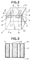
- a rectangular parallelepipedic dielectric ceramic block 1 made of a dielectric ceramic composite having a high dielectric constant and a low loss rate such as BaO-TiO 2 or BaO-TiO 2 -rare earth element, through which a pair of resonance holes 2 and 2 are vertically bored to produce openings at the top surface 1a and the bottom surface 1b of the ceramic block 1, a conductor layer 3 arranged on entire surface of the ceramic block 1 except the top surface 1a of the ceramic block 1, or on the four lateral side surfaces, the bottom surface 1b of the ceramic block 1 and the inner surfaces of the resonance holes 2 and 2, a pair of input and output terminals 4 and 4 arranged vis-a-vis the respective resonance holes 2, 2 along the upper edge of a lateral side surface 1c of the ceramic block 1, and a pair of trimming or capacitance regulating electrodes 5 and 5 arranged on the top surface 1a of the ceramic block 1.
- a pair of resonance holes 2 and 2 are vertically bored to produce openings at the top surface 1a and the bottom surface 1b of
- the conductor layer 3 may be formed by depositing metal material having a high conductivity such as silver or copper on the surfaces of the dielectric ceramic block 1 except the top surface 1a of the dielectric ceramic block 1.
- Each of said trimming electrodes 5 and 5 has an end connected to the corresponding input or output terminal 4 and the other end extending to the vicinity of the corresponding resonance hole 2, so that the embodiment may have a desired input and a desired output coupling capacitance by securing appropriate gaps 6 and 6 between the trimming electrodes 5 and 5 and the respective edges of the resonance holes 2 and 2.
- the input and the output coupling capacitance of a dielectric filter having a configuration as described above is a function of the size of the gaps 6 and 6 and the specific dielectric constant of the dielectric ceramic composite of the ceramic block 1, the dielectric filter, when manufactured, does not necessarily show a desired input and a desired output coupling capacitance because they are subject to errors that may take place during the manufacturing process.
- the capacitance across each of the gaps 6 and 6 is measured for the embodiment by using a capacitance gauge 7 which is connected between the corresponding one of the input and output terminals 4 and 4 and that of the resonance holes 2 and 2. If the capacitance exceeds a predetermined level, an appropriate front end portion 5' of the corresponding trimming electrode 5 is cut out by using a laser, a cutting tool or some other appropriate means to enlarge the gap 6. If, on the other hand, the capacitance falls short of the predetermined level, a small piece of conductor (not shown) is added to the front end of the trimming electrode 5 to reduce the gap 6.
- Fig. 6 is a partial perspective view of an alternative trimming electrode that can be used for the embodiment of Fig. 1 and is actually composed of a plurality of small pieces 5a through 5d.
- the capacitance of the gap 6 separating the trimming electrode 5 and the corresponding resonance hole 2 is measured by means of the capacitance gauge 7 connected between the corresponding input or output terminal 4 and the resonance hole 2, and is regulated by applying a conductive paint 8 such as one made of pasty silver between, for instance, the pieces 5a and 5b to electrically connect them until a desired capacitance level is achieved.
- each of the resonance holes 2 and 2 is grounded by the conductor layer 3 covering the bottom surface of the ceramic block 1 while the other end is electrically insulated by the exposed (dotted) top surface of the ceramic block 1 in the above embodiment.
- Fig. 7 illustrates another embodiment of the invention which is an interdigital type dielectric filter having three resonance holes 2, 2 and 2, which are alternately grounded on the top surface 1a and the bottom surface 1b of the ceramic block 1 by way of respective conductor layers 3a, 3b and 3c connected to respective ends of the resonance holes, while the remaining ends of the resonance holes are electrically insulated by the respective exposed (dotted) areas of the top and the bottom surfaces of the ceramic block 1.
- a pair of trimming electrodes 5 and 5 are arranged so as to be connected to respective input and output terminals 4 and 4 and extended toward the respective outer resonance holes 2 and 2 and a desired coupling capacitance may be produced at each of the gaps 6 and 6 separating the input and output terminals 4 and 4 and the resonance holes 2 and 2 by appropriately trimming the trimming electrodes 5 and 5.
- the concept of the present invention can be applied not only to dielectric filters having a pair of resonance holes, as in the case of the first embodiment, but also to those having three or more resonance holes as shown in Fig. 7.
- each of the trimming electrodes may be connected at an end to the corresponding resonance hole and separated at the other end from an edge of the corresponding input or output terminal to produce a gap for coupling capacitance.
- the once established coupling capacitance may be varied when the dielectric filter is turned upside down on a printed circuit board and soldered to related circuits of the board as the gaps may be partly filled with solder.
- a dielectric filter according to the present invention and having a configuration as described above by way of embodiments is free from such a problem because the gaps are located close to the respective resonance holes and hence remote from the top surface of the printed circuit board if the filter is partly contaminated with solder.
- a dielectric filter according to the present invention is provided with trimming electrodes arranged respectively between its input and output terminals and resonance holes to regulate the coupling capacitance, a desired input and a desired output coupling capacitance can be easily achieved for the filter.
- high quality dielectric filters can be provided at low cost on an industrial basis.
Landscapes
- Physics & Mathematics (AREA)
- Electromagnetism (AREA)
- Control Of Motors That Do Not Use Commutators (AREA)
Claims (3)
- Filtre diélectrique comportant un bloc de céramique diélectrique (1) en parallélépipède rectangle pourvu d'au moins deux trous (2) de résonance percés verticalement à travers lui, et une couche conductrice (3) formée sur la surface du bloc céramique (1), caractérisé en ce que la couche conductrice (3) est formée sur toute la surface du bloc céramique (1) à l'exception de la totalité, ou d'une partie, de la surface supérieure (1a) du bloc céramique (1), le filtre étant en outre caractérisé par : deux bornes (4) d'entrée et de sortie disposées chacune sur une première surface (1c) d'un côté latéral du bloc céramique (1), dans lequel des électrodes (5) d'ajustement sont prévues sur la surface supérieure (1a) ou sur les surfaces supérieure et inférieure du bloc céramique, s'étendant chacune depuis l'une, respective, desdites bornes (4) d'entrée et de sortie jusqu'à une région adjacente à l'ouverture du trou de résonance correspondant (2) sur le même côté, afin de réaliser un couplage capacitif entre chacune des bornes (4) d'entrée et de sortie et le trou de résonance correspondant (2).
- Filtre diélectrique selon la revendication 1, dans lequel chacune desdites électrodes (5) d'ajustement comporte un élément conducteur unique qui est pourvu d'un conducteur additionnel pour réguler la capacité de couplage en entrée et en sortie du filtre.
- Filtre diélectrique selon la revendication 1, dans lequel chacune desdites électrodes d'ajustement (5) comporte plusieurs petites pièces conductrices (5a, 5b, 5c, 5d) qui sont pontées électriquement par une peinture conductrice (8) pour l'obtention d'une capacité de couplage prédéterminée en entrée et prédéterminée en sortie.
Applications Claiming Priority (3)
| Application Number | Priority Date | Filing Date | Title |
|---|---|---|---|
| JP4468693U | 1993-07-23 | ||
| JP044686U JPH0711002U (ja) | 1993-07-23 | 1993-07-23 | 誘電体フィルタ |
| JP44686/93U | 1993-07-23 |
Publications (2)
| Publication Number | Publication Date |
|---|---|
| EP0635897A1 EP0635897A1 (fr) | 1995-01-25 |
| EP0635897B1 true EP0635897B1 (fr) | 1999-09-29 |
Family
ID=12698317
Family Applications (1)
| Application Number | Title | Priority Date | Filing Date |
|---|---|---|---|
| EP94305424A Expired - Lifetime EP0635897B1 (fr) | 1993-07-23 | 1994-07-22 | Filtre diélectrique |
Country Status (5)
| Country | Link |
|---|---|
| US (1) | US5818311A (fr) |
| EP (1) | EP0635897B1 (fr) |
| JP (1) | JPH0711002U (fr) |
| KR (1) | KR0177189B1 (fr) |
| DE (1) | DE69420911T2 (fr) |
Families Citing this family (8)
| Publication number | Priority date | Publication date | Assignee | Title |
|---|---|---|---|---|
| EP1119070B1 (fr) * | 1995-11-16 | 2003-08-27 | NGK Spark Plug Co. Ltd. | Filtre diélectrique et méthode d' ajustement de sa fréquence centrale |
| JPH1022710A (ja) * | 1996-07-03 | 1998-01-23 | Ngk Spark Plug Co Ltd | 誘電体フィルタの電極形成方法 |
| US6081174A (en) * | 1997-03-14 | 2000-06-27 | Taiyo Yuden Co., Ltd. | Wave filter having two or more coaxial dielectric resonators in juxtaposition |
| KR100299052B1 (ko) * | 1998-08-21 | 2001-10-27 | 오길록 | 무선통신시스템용대역통과필터 |
| DE60032300T2 (de) | 1999-09-24 | 2007-06-28 | NGK Spark Plug Co., Ltd., Nagoya | Dielektrisches Filter und dessen Herstellungsverfahren |
| JP2003087010A (ja) * | 2001-09-06 | 2003-03-20 | Ngk Spark Plug Co Ltd | 誘電体デュプレクサ |
| KR101504957B1 (ko) * | 2013-08-13 | 2015-03-23 | 한국광성전자 주식회사 | 세라믹 모노 블록 및 이를 이용한 세라믹 필터의 입출력단자 및 상면 패턴 형성 방법 |
| KR20220037225A (ko) * | 2020-09-17 | 2022-03-24 | 주식회사 엘지에너지솔루션 | 우수한 방열 성능을 구비한 버스바 |
Family Cites Families (16)
| Publication number | Priority date | Publication date | Assignee | Title |
|---|---|---|---|---|
| JPS5773501A (en) * | 1980-10-25 | 1982-05-08 | Fujitsu Ltd | Dielectric filter element and dielectric filter |
| US4462098A (en) * | 1982-02-16 | 1984-07-24 | Motorola, Inc. | Radio frequency signal combining/sorting apparatus |
| JPS6052102A (ja) * | 1983-09-01 | 1985-03-25 | Oki Electric Ind Co Ltd | 誘電体共振器および誘電体共振器の共振周波数の調整方法 |
| JPS60114004A (ja) * | 1983-11-25 | 1985-06-20 | Murata Mfg Co Ltd | 誘電体フィルタの実装構造 |
| US4675632A (en) * | 1984-02-23 | 1987-06-23 | Mitsubishi Denki Kabushiki Kaisha | Coaxial line shape resonator with high dielectric constant |
| JPS6238601A (ja) * | 1985-08-13 | 1987-02-19 | Murata Mfg Co Ltd | インタ−デジタル型フイルタおよびその製造方法 |
| JPS63110801A (ja) * | 1986-10-28 | 1988-05-16 | Murata Mfg Co Ltd | アクテイブフイルタ |
| US4800348A (en) * | 1987-08-03 | 1989-01-24 | Motorola, Inc. | Adjustable electronic filter and method of tuning same |
| JPH0642602B2 (ja) * | 1987-09-10 | 1994-06-01 | 三菱電機株式会社 | 誘電体フィルタ |
| JPH02241203A (ja) * | 1989-03-15 | 1990-09-25 | Matsushita Electric Ind Co Ltd | 同軸共振器およびそれを用いたフィルタ |
| JPH04150101A (ja) * | 1990-10-08 | 1992-05-22 | Murata Mfg Co Ltd | 誘電体共振器 |
| US5327108A (en) * | 1991-03-12 | 1994-07-05 | Motorola, Inc. | Surface mountable interdigital block filter having zero(s) in transfer function |
| US5198788A (en) * | 1991-11-01 | 1993-03-30 | Motorola, Inc. | Laser tuning of ceramic bandpass filter |
| US5208566A (en) * | 1992-01-21 | 1993-05-04 | Motorola, Inc. | Dielectric filter having adjacently-positioned resonators of dissimilar cross-sectional dimensions and notched side surface |
| EP0552761B1 (fr) * | 1992-01-23 | 1999-07-07 | Murata Manufacturing Co., Ltd. | Filtre diélectrque et son procédé the fabrication |
| JPH06164205A (ja) * | 1992-11-17 | 1994-06-10 | Oki Electric Ind Co Ltd | 誘電体フィルタ |
-
1993
- 1993-07-23 JP JP044686U patent/JPH0711002U/ja active Pending
-
1994
- 1994-07-21 US US08/277,277 patent/US5818311A/en not_active Expired - Fee Related
- 1994-07-21 KR KR1019940017604A patent/KR0177189B1/ko not_active Expired - Fee Related
- 1994-07-22 EP EP94305424A patent/EP0635897B1/fr not_active Expired - Lifetime
- 1994-07-22 DE DE69420911T patent/DE69420911T2/de not_active Expired - Fee Related
Also Published As
| Publication number | Publication date |
|---|---|
| KR950004628A (ko) | 1995-02-18 |
| DE69420911T2 (de) | 2000-02-03 |
| US5818311A (en) | 1998-10-06 |
| EP0635897A1 (fr) | 1995-01-25 |
| KR0177189B1 (ko) | 1999-05-15 |
| JPH0711002U (ja) | 1995-02-14 |
| DE69420911D1 (de) | 1999-11-04 |
Similar Documents
| Publication | Publication Date | Title |
|---|---|---|
| US6046409A (en) | Multilayer microelectronic circuit | |
| US6078230A (en) | Characteristic adjusting method for dielectric filter using a grinding tool | |
| JPH0728165B2 (ja) | セラミック帯域フィルタ | |
| US5349314A (en) | Stripline filter device having a coupling dielectric layer between two stripline resonators | |
| EP1439599B1 (fr) | Filtre diélectrique de type guide d'ondes | |
| US5929726A (en) | Dielectric filter device | |
| US6310525B1 (en) | Dielectric laminated device and its manufacturing method | |
| EP0343345B1 (fr) | Filtre en technique de ligne à bande | |
| US5187455A (en) | Delay line device with adjustable time delay | |
| EP0635897B1 (fr) | Filtre diélectrique | |
| US5825262A (en) | Ladder filter with piezoelectric resonators each having a plurality of layers with internal electrodes | |
| EP0414619B1 (fr) | Procédé de réglage de la réponse en fréquence d'un dispositif à filtrage du type à trois conducteurs | |
| EP0897217A2 (fr) | Filtre piézoélectrique à piégeage d'énergie | |
| EP0746052A1 (fr) | Filtre diélectrique | |
| US5291162A (en) | Method of adjusting frequency response in a microwave strip-line filter device | |
| US5945895A (en) | Resonant frequency compensated dielectric filter | |
| US5831497A (en) | Dielectirc resonator apparatus | |
| EP0568370B1 (fr) | Dispositif à filtrage diélectrique | |
| EP0532770B1 (fr) | Filtre ligne triplaque hyperfrequence | |
| US6924707B2 (en) | Resonator | |
| US6005456A (en) | Dielectric filter having non-conductive adjusting regions | |
| US6392505B1 (en) | Dielectric device | |
| EP0837518B1 (fr) | Filtre diélectrique | |
| US6034579A (en) | Dielectric filter of the band elimination type | |
| JP3159025B2 (ja) | 誘電体フィルタ |
Legal Events
| Date | Code | Title | Description |
|---|---|---|---|
| PUAI | Public reference made under article 153(3) epc to a published international application that has entered the european phase |
Free format text: ORIGINAL CODE: 0009012 |
|
| AK | Designated contracting states |
Kind code of ref document: A1 Designated state(s): DE FR GB |
|
| 17P | Request for examination filed |
Effective date: 19950512 |
|
| 17Q | First examination report despatched |
Effective date: 19970808 |
|
| GRAG | Despatch of communication of intention to grant |
Free format text: ORIGINAL CODE: EPIDOS AGRA |
|
| GRAG | Despatch of communication of intention to grant |
Free format text: ORIGINAL CODE: EPIDOS AGRA |
|
| GRAH | Despatch of communication of intention to grant a patent |
Free format text: ORIGINAL CODE: EPIDOS IGRA |
|
| GRAH | Despatch of communication of intention to grant a patent |
Free format text: ORIGINAL CODE: EPIDOS IGRA |
|
| GRAA | (expected) grant |
Free format text: ORIGINAL CODE: 0009210 |
|
| AK | Designated contracting states |
Kind code of ref document: B1 Designated state(s): DE FR GB |
|
| REF | Corresponds to: |
Ref document number: 69420911 Country of ref document: DE Date of ref document: 19991104 |
|
| ET | Fr: translation filed | ||
| PLBE | No opposition filed within time limit |
Free format text: ORIGINAL CODE: 0009261 |
|
| STAA | Information on the status of an ep patent application or granted ep patent |
Free format text: STATUS: NO OPPOSITION FILED WITHIN TIME LIMIT |
|
| 26N | No opposition filed | ||
| REG | Reference to a national code |
Ref country code: GB Ref legal event code: IF02 |
|
| PGFP | Annual fee paid to national office [announced via postgrant information from national office to epo] |
Ref country code: FR Payment date: 20040708 Year of fee payment: 11 |
|
| PGFP | Annual fee paid to national office [announced via postgrant information from national office to epo] |
Ref country code: GB Payment date: 20040721 Year of fee payment: 11 |
|
| PGFP | Annual fee paid to national office [announced via postgrant information from national office to epo] |
Ref country code: DE Payment date: 20040729 Year of fee payment: 11 |
|
| PG25 | Lapsed in a contracting state [announced via postgrant information from national office to epo] |
Ref country code: GB Free format text: LAPSE BECAUSE OF NON-PAYMENT OF DUE FEES Effective date: 20050722 |
|
| PG25 | Lapsed in a contracting state [announced via postgrant information from national office to epo] |
Ref country code: DE Free format text: LAPSE BECAUSE OF NON-PAYMENT OF DUE FEES Effective date: 20060201 |
|
| GBPC | Gb: european patent ceased through non-payment of renewal fee |
Effective date: 20050722 |
|
| PG25 | Lapsed in a contracting state [announced via postgrant information from national office to epo] |
Ref country code: FR Free format text: LAPSE BECAUSE OF NON-PAYMENT OF DUE FEES Effective date: 20060331 |
|
| REG | Reference to a national code |
Ref country code: FR Ref legal event code: ST Effective date: 20060331 |