EP0415047B1 - Circuit de temporisation de précision - Google Patents
Circuit de temporisation de précision Download PDFInfo
- Publication number
- EP0415047B1 EP0415047B1 EP90113404A EP90113404A EP0415047B1 EP 0415047 B1 EP0415047 B1 EP 0415047B1 EP 90113404 A EP90113404 A EP 90113404A EP 90113404 A EP90113404 A EP 90113404A EP 0415047 B1 EP0415047 B1 EP 0415047B1
- Authority
- EP
- European Patent Office
- Prior art keywords
- circuit
- clock
- transistors
- coupled
- pair
- Prior art date
- Legal status (The legal status is an assumption and is not a legal conclusion. Google has not performed a legal analysis and makes no representation as to the accuracy of the status listed.)
- Expired - Lifetime
Links
- 239000003990 capacitor Substances 0.000 claims description 24
- 238000007599 discharging Methods 0.000 claims description 2
- 239000004065 semiconductor Substances 0.000 claims description 2
- 230000008878 coupling Effects 0.000 claims 2
- 238000010168 coupling process Methods 0.000 claims 2
- 238000005859 coupling reaction Methods 0.000 claims 2
- 230000000295 complement effect Effects 0.000 claims 1
- 230000001419 dependent effect Effects 0.000 claims 1
- 230000007704 transition Effects 0.000 description 6
- 238000010586 diagram Methods 0.000 description 4
- 238000000034 method Methods 0.000 description 2
- 230000003750 conditioning effect Effects 0.000 description 1
- 230000000694 effects Effects 0.000 description 1
- 230000007257 malfunction Effects 0.000 description 1
- 230000000630 rising effect Effects 0.000 description 1
- 230000035945 sensitivity Effects 0.000 description 1
Images

Classifications
-
- H—ELECTRICITY
- H03—ELECTRONIC CIRCUITRY
- H03K—PULSE TECHNIQUE
- H03K5/00—Manipulating of pulses not covered by one of the other main groups of this subclass
- H03K5/13—Arrangements having a single output and transforming input signals into pulses delivered at desired time intervals
- H03K5/135—Arrangements having a single output and transforming input signals into pulses delivered at desired time intervals by the use of time reference signals, e.g. clock signals
Definitions
- timing edges upon which all the sequential events are based.
- various techniques to produce such timing edges by delaying one or more edges of a reference clock signal, such as using RC circuits or delay lines.
- the prior art circuits however had problems with noise and accuracy due to sensitivity to temperature and process variations in the making of the devices comprising the delay circuit. These problems caused the delay generated to vary. Such variations can cause digital logic systems to malfunction.
- voltage controlled oscillators used voltage controlled oscillators to provide control voltages to the controlled stages of tapped delay lines or used multiple capacitors that were varied with switches. Such other systems encountered similar problems and had undesirable side effects.
- the present invention resolves these problems with a precision, compact, low power timing circuit that generates substantially noise free and temperature insensitive precision timing edges which are not multiples or fractions of the timing clock and does this, without the need for precision analog capability, by a ratio capacitor circuit.
- the present invention is superior to those circuits known in the prior art since it is not limited to multiples or fractions of the main clock frequency, yet is more stable, less prone to noise problems, simpler, cheaper and easier to build than the prior art circuits while having the capability of being self calibrating, readily adjustable, faster and easily extendable with an accuracy independent of the absolute value of the components used.
- the present invention comprises a ratio circuit coupled to a clock and a control current generator.
- the ratio circuit utilizes at least two capacitors each of which is coupled in series with a respective transistor and arranged in parallel with one another. Each capacitor transistor pair is in parallel to the other and coupled between the control current generator and ground so that at least one of the transistors in a selected capacitor transistor series can be selectively turned off while the other is directly controlled by the clock cycle.
- Means for charging and discharging the capacitors are included in the circuit.
- the present invention is thus a circuit, for generating timing edges within a clock cycle which timing edges can be any function of the clock cycle.
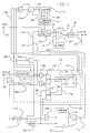
- Fig. 1 illustrates an overall block diagram of a system using the ratio circuit of the invention.
- Fig. 2 illustrates a detailed schematic of the ratio circuit of the present invention.
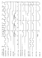
- Fig. 3 is a timing diagram showing pulses appearing at various nodes of the circuit of Fig. 1.
- Fig. 1 there is shown a block diagram of a circuit for obtaining precision timing pulses independent of the input clock signals used.
- this circuit comprises a counter 10 for counting a designated number of transitions and, at selected times, causing a current source circuit 11 to send selected current levels to a ratio circuit 12.
- a control logic circuit 13 which is comprised of a counter 13a, two AND circuits 13b and 13c, two OR circuits 13d, and 13m, a differentiating circuit 13e and a latch circuit 13f, sends a control signal on line 13h and a reset signal on line 13k to the ratio circuit 12.
- the counter 13a of the control logic circuit 13 is coupled to a clock 50, to AND circuit 13b, and via line 60 to a first input of a three input AND circuit 14 whose output is directed through inverter 14a into counter 10.
- the clock 50 is coupled not only to the counter 13a but also, through invertor 50a, to the AND circuits 13b and 13c, and to a differentiating circuit 17.
- a test signal source 16 is coupled directly to the ratio circuit 12, to the AND circuits 14 and 13b, to differentiating circuit 18b and through an inverter 16a to the AND circuit 13c.
- the differentiating circuit 18b is coupled to reset of latch 13f through OR 13m.
- the ratio circuit 12 is coupled to an input 21a of a differential amplifier 21 which has a reference voltage source 23 coupled to its other input 21b.
- the output 21c of this differential amplifier 21 is in turn transmitted through a differentiating circuit 24 to the circuit output 25, and thence to the latch 13f through OR 13m of the control logic circuit 13, and also to the compare latch 18 through AND gate 18a.
- the output of AND 13b is connected to OR 13d, with the output of AND 13c connected to the other input of OR 13d.
- the output of OR 13d is connected through differentiating circuit 13e to latch 13f.
- the output of the differentiating circuit 17 is connected to a latch 18 through an AND circuit 18a where the output of the differentiating circuit 17 is anded with the output 25 to set latch 18, which is reset by to the output of the differentiating circuit 18b.
- the output of latch 18 is inverted by inverter 19 and coupled into a second input of AND circuit 14.
- the ratio circuit 12 of Fig. 1 is shown in greater detail in schematic form in Fig. 2. As shown in Fig. 2 this circuit is comprised of six transistors Q1, Q2, Q3, Q4, Q5 and Q6 together with two capacitors C1 and C2 of different capacitive value and an AND gate 30. If desired, it should be clearly understood that this AND gate 30 could be separate from and outside of the ratio circuit itself.
- the test signal 16 is supplied into the AND gate 30 together with the signal from latch 13f on line 13h.
- This latching signal line 13h is also connected to the gates of transistors Q1 and Q6.
- the other line 13k from latch 13f is connected to the gates of transistors Q3, Q4 and Q5.
- the output of AND gate 30 is coupled to the gate of transistor Q2.
- transistors Q1 and Q2 have their sources coupled to a common node B and their drains coupled to ground through respective capacitors C1 and C2 and respective reset transistors Q3 and Q4.
- Transistor Q6 has its source coupled to the output from the current source circuit 11 and its drain coupled to node B while transistor Q5 has its source coupled to node B and its drain coupled to ground.
- Fig. 3 shows a timing diagram setting forth the pulses seen at by selected nodes and circuits set forth in Figs. 1 and 2.
- the AND circuit 14 With positive input signals received, from counter 13a on line 60, from the test source 16, and the inverter 19 on line 14b, the AND circuit 14 emits a positive signal which is inverted by the inverter 14a and passed as a negative signal into the counter 10 via line 14e. Since counter 10 decrements only when a positive transition is received on its input line 14e no change in the status of counter 10 occurs. Also at time T1 the output line 13h of latch circuit 13f goes low holding transistors Q1 and Q6 off, and line 13k is now high turning on transistors Q3, Q4 and Q5 causing node B to remain low and the capacitors C1 and C2 remain discharged. At this time T1 the circuit is initialized and ready for operation.
- the AND gate 18a is not enabled and the pulse from the differentiator circuit 17 is not coincident in time with the output line 25.
- the AND gate 18a is not enabled and compare latch 18 remains in its unset or low condition.
- the compare latch 18 is now set with line 18c being high and causes external circuits (not shown) to reset the test circuit 16 on the next positive transition time T14 of clock 50, thus disabling the AND gate 13b and the AND gate 14, but enabling the AND gate 13c for normal operations.
- the capacitors C1 and C2 can be either of equal values or of different value depending on the ratio desired.
Landscapes
- Physics & Mathematics (AREA)
- Nonlinear Science (AREA)
- Manipulation Of Pulses (AREA)
Claims (9)
- Circuit pour produire des fronts de synchronisation à l'intérieur d'un cycle d'horloge comprenant :
une horloge (50) pour produire une pluralité de cycles d'horloge d'une fréquence sélectionnée, une source de signal de test (16), un générateur de courant commandable (11) couplé à l'horloge (50) et à la source de signal de test (16) pour produire une pluralité de courants en fonction du mode de fonctionnement déterminé par l'horloge (50) et par la source de signal de test (16),
un circuit de rapport couplé à l'horloge (50), au générateur de courant (11) à la source de signal test (16) et un noeud de sortie (25),
circuit de rapport (12) comprenant :
une paire de transistors (Q1, Q2), dont chaque trajet de courant est couplé en série à un condensateur respectif (C1, C2) qui doit être chargé à une extrémité en commun au générateur de courant et au noeud de sortie (25),
un transistor (Q1) de la paire de transistors (Q1, Q2) ayant son électrode de commande couplée (13h) à l'horloge (50), et
l'autre transistor de la paire de transistors (Q1, Q2) ayant son électrode de commande couplée à un signal représentant une combinaison logique du signal de test et à l'horloge (50) et étant sélectivement rendu conducteur,
un moyen de commutation (Q3, Q4) pour décharger chacun des condensateurs (C1, C2),
un circuit de commande (13, 18) répondant au signal d'horloge, au signal de test et un signal de contre-réaction provenant des noeuds de sortie (25), étant couplé aux électrodes de commande de la paire de transistors (Q1, Q2) et au moyen de commutation (Q3, Q4), le circuit de commande délivrant des signaux complémentaires à la paire de transistors (Q1, Q2) et au moyen de commutation (Q3, Q4) de manière telle qu'en fonction du signal délivré par la source de signal de test, un ou les deux condensateurs parmi lesdits premier et second condensateurs sont chargés à partir de la source de courant par l'intermédiaire d'un transistor respectif de ladite paire de transistors (Q1, Q2). - Circuit selon la revendication 1, dans lequel le circuit de commande (13, 18) comprend un moyen de bascule (13f).
- Circuit selon l'une quelconque des revendications ci-dessus dans lequel
le circuit de commande (13, 18) comprend un circuit ET, et
l'autre transistor (Q2) de la paire de transistors (Q1, Q2) est couplé à et commandé par l'horloge (50) et par le signal de source (16) par l'intermédiaire du circuit ET (30). - Circuit selon l'une quelconque des revendications ci-dessus, dans lequel il est de plus prévu un amplificateur opérationnel (21) couplé à la paire de transistors (Q1, Q2) et à une source de tension de référence (23).
- Circuit selon l'une quelconque des revendications ci-dessus, dans lequel un générateur de courant (11) comporte un moyen pour produire ladite pluralité de courants sur des séquences de temps variables.
- Circuit selon l'une quelconque des revendications ci-dessus, comprenant de plus
un premier circuit de contre-réaction (13m) couplant le noeud de sortie (25) au circuit de commande (13) pour remettre à zéro le circuit de commande (13) lorsque les fronts de synchronisation se produisent. - Circuit selon l'une quelconque des revendications ci-dessus, comprenant de plus
un second circuit de contre-réaction (18) couplant le noeud de sortie (25) et l'horloge (50) afin de délivrer un signal (sortie 18a) lorsque le cycle d'horloge et les fronts de synchronisation coïncident dans le temps. - Circuit selon la revendication 7, comprenant de plus un moyen de compteur (10) couplé au générateur de courant (11) pour faire varier le générateur de courant (11) à des fins d'auto-étalonnage du circuit lorsque le signal (sortie 18a) est délivré.
- Circuit selon l'une quelconque des revendications ci-dessus, dans lequel les transistors (Q1, Q2, Q3 et Q4) et les condensateurs (C1 et C2) sont placés dans la même puce semi-conductrice.
Applications Claiming Priority (2)
| Application Number | Priority Date | Filing Date | Title |
|---|---|---|---|
| US40060489A | 1989-08-30 | 1989-08-30 | |
| US400604 | 1989-08-30 |
Publications (3)
| Publication Number | Publication Date |
|---|---|
| EP0415047A2 EP0415047A2 (fr) | 1991-03-06 |
| EP0415047A3 EP0415047A3 (en) | 1991-05-08 |
| EP0415047B1 true EP0415047B1 (fr) | 1995-04-05 |
Family
ID=23584275
Family Applications (1)
| Application Number | Title | Priority Date | Filing Date |
|---|---|---|---|
| EP90113404A Expired - Lifetime EP0415047B1 (fr) | 1989-08-30 | 1990-07-13 | Circuit de temporisation de précision |
Country Status (3)
| Country | Link |
|---|---|
| EP (1) | EP0415047B1 (fr) |
| JP (1) | JPH0612502B2 (fr) |
| DE (1) | DE69018343T2 (fr) |
Families Citing this family (3)
| Publication number | Priority date | Publication date | Assignee | Title |
|---|---|---|---|---|
| US5548249A (en) * | 1994-05-24 | 1996-08-20 | Matsushita Electric Industrial Co., Ltd. | Clock generator and method for generating a clock |
| JP2003079214A (ja) * | 2001-09-13 | 2003-03-18 | Yanmar Agricult Equip Co Ltd | 移植機の予備苗台 |
| US10320374B2 (en) * | 2017-04-17 | 2019-06-11 | Ciena Corporation | Fine resolution high speed linear delay element |
Family Cites Families (1)
| Publication number | Priority date | Publication date | Assignee | Title |
|---|---|---|---|---|
| US3906247A (en) * | 1974-01-16 | 1975-09-16 | Gte Automatic Electric Lab Inc | Programmable proportional clock edge delay circuit |
-
1990
- 1990-07-13 DE DE1990618343 patent/DE69018343T2/de not_active Expired - Fee Related
- 1990-07-13 EP EP90113404A patent/EP0415047B1/fr not_active Expired - Lifetime
- 1990-08-16 JP JP2215113A patent/JPH0612502B2/ja not_active Expired - Lifetime
Non-Patent Citations (1)
| Title |
|---|
| TTL Data Book, Texas Instruments 1979, pages 6-24 and 6-25 * |
Also Published As
| Publication number | Publication date |
|---|---|
| DE69018343T2 (de) | 1995-10-12 |
| JPH0612502B2 (ja) | 1994-02-16 |
| EP0415047A3 (en) | 1991-05-08 |
| EP0415047A2 (fr) | 1991-03-06 |
| JPH0392913A (ja) | 1991-04-18 |
| DE69018343D1 (de) | 1995-05-11 |
Similar Documents
| Publication | Publication Date | Title |
|---|---|---|
| US4291274A (en) | Phase detector circuit using logic gates | |
| US4417158A (en) | Clock generator circuit | |
| US3961269A (en) | Multiple phase clock generator | |
| KR0133164B1 (ko) | 반도체 소자의 입력 전이 검출회로 | |
| US5028888A (en) | Multistage current-controlled oscillator | |
| JPH0799430A (ja) | モノリシック集積パッド駆動装置の出力電流設定方法 | |
| US4355283A (en) | Circuit and method for duty cycle control | |
| EP0415047B1 (fr) | Circuit de temporisation de précision | |
| US5093584A (en) | Self calibrating timing circuit | |
| JP3963421B2 (ja) | 制御発振システムとその方法 | |
| US4779063A (en) | Oscillator with feedback loop including delay circuit | |
| JPH08172354A (ja) | 位相ロック・ループ回路におけるチャージ・ポンプ構造および電流供給方法 | |
| US5384554A (en) | Voltage controlled oscillator circuit employing integrated circuit component ratios | |
| US3657557A (en) | Synchronous binary counter | |
| JPH0879063A (ja) | 位相ロック・ループ回路およびパルス供給/生成方法 | |
| JP3256057B2 (ja) | 位相同期ループ回路装置およびその位相比較器 | |
| US3461404A (en) | Disconnectable pulse generator | |
| WO2002015382A2 (fr) | Oscillateur a sensibilite reduite aux changements de tension d'alimentation | |
| US3566301A (en) | Multivibrator with linearly variable voltage controlled duty cycle | |
| US4293780A (en) | Digital integrated semiconductor circuit | |
| JP2611542B2 (ja) | 可変分周回路 | |
| US3517211A (en) | Frequency divider circuit | |
| SU1026288A1 (ru) | Многофазный генератор импульсов | |
| US4015141A (en) | Apparatus for comparing voltages | |
| JP3673037B2 (ja) | 波形整形回路 |
Legal Events
| Date | Code | Title | Description |
|---|---|---|---|
| PUAI | Public reference made under article 153(3) epc to a published international application that has entered the european phase |
Free format text: ORIGINAL CODE: 0009012 |
|
| 17P | Request for examination filed |
Effective date: 19901213 |
|
| AK | Designated contracting states |
Kind code of ref document: A2 Designated state(s): DE FR GB |
|
| PUAL | Search report despatched |
Free format text: ORIGINAL CODE: 0009013 |
|
| AK | Designated contracting states |
Kind code of ref document: A3 Designated state(s): DE FR GB |
|
| 17Q | First examination report despatched |
Effective date: 19930510 |
|
| GRAA | (expected) grant |
Free format text: ORIGINAL CODE: 0009210 |
|
| AK | Designated contracting states |
Kind code of ref document: B1 Designated state(s): DE FR GB |
|
| REF | Corresponds to: |
Ref document number: 69018343 Country of ref document: DE Date of ref document: 19950511 |
|
| PGFP | Annual fee paid to national office [announced via postgrant information from national office to epo] |
Ref country code: GB Payment date: 19950622 Year of fee payment: 6 |
|
| ET | Fr: translation filed | ||
| PGFP | Annual fee paid to national office [announced via postgrant information from national office to epo] |
Ref country code: FR Payment date: 19950704 Year of fee payment: 6 |
|
| PGFP | Annual fee paid to national office [announced via postgrant information from national office to epo] |
Ref country code: DE Payment date: 19950720 Year of fee payment: 6 |
|
| PLBE | No opposition filed within time limit |
Free format text: ORIGINAL CODE: 0009261 |
|
| STAA | Information on the status of an ep patent application or granted ep patent |
Free format text: STATUS: NO OPPOSITION FILED WITHIN TIME LIMIT |
|
| 26N | No opposition filed | ||
| PG25 | Lapsed in a contracting state [announced via postgrant information from national office to epo] |
Ref country code: GB Effective date: 19960713 |
|
| GBPC | Gb: european patent ceased through non-payment of renewal fee |
Effective date: 19960713 |
|
| PG25 | Lapsed in a contracting state [announced via postgrant information from national office to epo] |
Ref country code: FR Effective date: 19970328 |
|
| PG25 | Lapsed in a contracting state [announced via postgrant information from national office to epo] |
Ref country code: DE Effective date: 19970402 |
|
| REG | Reference to a national code |
Ref country code: FR Ref legal event code: ST |