EP0415094A2 - Boîte d'alignement à fibres multiples pour composants opto-électroniques avec des facettes inclinées - Google Patents
Boîte d'alignement à fibres multiples pour composants opto-électroniques avec des facettes inclinées Download PDFInfo
- Publication number
- EP0415094A2 EP0415094A2 EP90114478A EP90114478A EP0415094A2 EP 0415094 A2 EP0415094 A2 EP 0415094A2 EP 90114478 A EP90114478 A EP 90114478A EP 90114478 A EP90114478 A EP 90114478A EP 0415094 A2 EP0415094 A2 EP 0415094A2
- Authority
- EP
- European Patent Office
- Prior art keywords
- fiber
- carrier
- package
- component
- facet
- Prior art date
- Legal status (The legal status is an assumption and is not a legal conclusion. Google has not performed a legal analysis and makes no representation as to the accuracy of the status listed.)
- Withdrawn
Links
- 239000000835 fiber Substances 0.000 title claims abstract description 115
- 230000005693 optoelectronics Effects 0.000 title claims abstract description 31
- 239000013307 optical fiber Substances 0.000 claims abstract description 97
- 238000000034 method Methods 0.000 claims abstract description 43
- 229910000679 solder Inorganic materials 0.000 claims abstract description 31
- 238000001816 cooling Methods 0.000 claims abstract description 29
- 238000005476 soldering Methods 0.000 claims abstract description 24
- 230000008878 coupling Effects 0.000 claims abstract description 23
- 238000010168 coupling process Methods 0.000 claims abstract description 23
- 238000005859 coupling reaction Methods 0.000 claims abstract description 23
- 230000008018 melting Effects 0.000 claims abstract description 13
- 238000002844 melting Methods 0.000 claims abstract description 13
- 239000000463 material Substances 0.000 claims description 4
- 239000004020 conductor Substances 0.000 claims description 3
- 239000007791 liquid phase Substances 0.000 claims description 3
- 239000007790 solid phase Substances 0.000 claims description 3
- 238000013461 design Methods 0.000 abstract description 10
- 239000002184 metal Substances 0.000 abstract description 3
- 229910052751 metal Inorganic materials 0.000 abstract description 3
- 238000004364 calculation method Methods 0.000 abstract description 2
- 239000006023 eutectic alloy Substances 0.000 abstract description 2
- 239000004065 semiconductor Substances 0.000 description 20
- 230000003287 optical effect Effects 0.000 description 14
- 239000012876 carrier material Substances 0.000 description 6
- 230000035945 sensitivity Effects 0.000 description 4
- 238000003466 welding Methods 0.000 description 4
- 238000013459 approach Methods 0.000 description 3
- 238000004806 packaging method and process Methods 0.000 description 3
- 239000000758 substrate Substances 0.000 description 2
- RYGMFSIKBFXOCR-UHFFFAOYSA-N Copper Chemical compound [Cu] RYGMFSIKBFXOCR-UHFFFAOYSA-N 0.000 description 1
- 239000004593 Epoxy Substances 0.000 description 1
- XUIMIQQOPSSXEZ-UHFFFAOYSA-N Silicon Chemical compound [Si] XUIMIQQOPSSXEZ-UHFFFAOYSA-N 0.000 description 1
- 229910045601 alloy Inorganic materials 0.000 description 1
- 239000000956 alloy Substances 0.000 description 1
- 230000003321 amplification Effects 0.000 description 1
- 238000003491 array Methods 0.000 description 1
- 238000000429 assembly Methods 0.000 description 1
- 230000000712 assembly Effects 0.000 description 1
- 239000000919 ceramic Substances 0.000 description 1
- 238000000576 coating method Methods 0.000 description 1
- 150000001875 compounds Chemical class 0.000 description 1
- 229910052802 copper Inorganic materials 0.000 description 1
- 239000010949 copper Substances 0.000 description 1
- 230000000694 effects Effects 0.000 description 1
- 238000005516 engineering process Methods 0.000 description 1
- 230000005496 eutectics Effects 0.000 description 1
- 238000002474 experimental method Methods 0.000 description 1
- 230000008014 freezing Effects 0.000 description 1
- 238000007710 freezing Methods 0.000 description 1
- 238000010438 heat treatment Methods 0.000 description 1
- 229910052738 indium Inorganic materials 0.000 description 1
- APFVFJFRJDLVQX-UHFFFAOYSA-N indium atom Chemical compound [In] APFVFJFRJDLVQX-UHFFFAOYSA-N 0.000 description 1
- 238000009413 insulation Methods 0.000 description 1
- 238000002955 isolation Methods 0.000 description 1
- 238000004519 manufacturing process Methods 0.000 description 1
- 238000003199 nucleic acid amplification method Methods 0.000 description 1
- 238000005457 optimization Methods 0.000 description 1
- 238000005192 partition Methods 0.000 description 1
- 238000012545 processing Methods 0.000 description 1
- 238000011160 research Methods 0.000 description 1
- 238000007789 sealing Methods 0.000 description 1
- 238000001338 self-assembly Methods 0.000 description 1
- 229910052710 silicon Inorganic materials 0.000 description 1
- 239000010703 silicon Substances 0.000 description 1
- 230000000087 stabilizing effect Effects 0.000 description 1
- 238000012360 testing method Methods 0.000 description 1
- 238000012546 transfer Methods 0.000 description 1
Images


Classifications
-
- G—PHYSICS
- G02—OPTICS
- G02B—OPTICAL ELEMENTS, SYSTEMS OR APPARATUS
- G02B6/00—Light guides; Structural details of arrangements comprising light guides and other optical elements, e.g. couplings
- G02B6/24—Coupling light guides
- G02B6/42—Coupling light guides with opto-electronic elements
- G02B6/4201—Packages, e.g. shape, construction, internal or external details
- G02B6/4219—Mechanical fixtures for holding or positioning the elements relative to each other in the couplings; Alignment methods for the elements, e.g. measuring or observing methods especially used therefor
- G02B6/4236—Fixing or mounting methods of the aligned elements
- G02B6/4238—Soldering
-
- G—PHYSICS
- G02—OPTICS
- G02B—OPTICAL ELEMENTS, SYSTEMS OR APPARATUS
- G02B6/00—Light guides; Structural details of arrangements comprising light guides and other optical elements, e.g. couplings
- G02B6/24—Coupling light guides
- G02B6/42—Coupling light guides with opto-electronic elements
- G02B6/4201—Packages, e.g. shape, construction, internal or external details
- G02B6/4202—Packages, e.g. shape, construction, internal or external details for coupling an active element with fibres without intermediate optical elements, e.g. fibres with plane ends, fibres with shaped ends, bundles
-
- G—PHYSICS
- G02—OPTICS
- G02B—OPTICAL ELEMENTS, SYSTEMS OR APPARATUS
- G02B6/00—Light guides; Structural details of arrangements comprising light guides and other optical elements, e.g. couplings
- G02B6/24—Coupling light guides
- G02B6/42—Coupling light guides with opto-electronic elements
- G02B6/4201—Packages, e.g. shape, construction, internal or external details
- G02B6/4249—Packages, e.g. shape, construction, internal or external details comprising arrays of active devices and fibres
-
- G—PHYSICS
- G02—OPTICS
- G02B—OPTICAL ELEMENTS, SYSTEMS OR APPARATUS
- G02B6/00—Light guides; Structural details of arrangements comprising light guides and other optical elements, e.g. couplings
- G02B6/24—Coupling light guides
- G02B6/42—Coupling light guides with opto-electronic elements
- G02B6/4201—Packages, e.g. shape, construction, internal or external details
- G02B6/4219—Mechanical fixtures for holding or positioning the elements relative to each other in the couplings; Alignment methods for the elements, e.g. measuring or observing methods especially used therefor
- G02B6/422—Active alignment, i.e. moving the elements in response to the detected degree of coupling or position of the elements
- G02B6/4225—Active alignment, i.e. moving the elements in response to the detected degree of coupling or position of the elements by a direct measurement of the degree of coupling, e.g. the amount of light power coupled to the fibre or the opto-electronic element
Definitions
- This invention relates to packaging of optoelectronic components which generate or process signals that pass through optical fibers.
- it addresses the critical need for providing stable, low-cost alignment of multiple optical fibers to a tilted facet optoelectronic component, such as an optical amplifier,and a standard package therefor.
- An optoelectronic package is a container or housing that provides protection and support for both active and passive components contained within it. These components and their interconnection define an optical-electrical circuit and the function of the package.
- the package also includes a means of connecting the internal components with the external environment, usually as electrical feed-through and optical fiber. This invention is directed both to the connection of the optical fiber to the tilted facet components within the package, and to positioning the optical fiber connecting means with respect to a standard package.
- optical fiber transmits light through its inner core, which is much smaller than the diameter of the optical fiber.
- optical fiber There are two classes of optical fiber presently used in packaging semiconductor devices: singlemode and multimode, with core diameters of 10 ⁇ m and 100 ⁇ m, respectively. Most telecommunication systems use singlemode fiber because it is superior in reducing noise arising from mode partition noise.
- One exemplary semiconductor devices requiring the coupling of multiple optical fibers includes an array of semiconductor lasers used as light sources for such purposes as parallel processing.
- An optical fiber must be coupled to the lasing output beam emitted from the active layer of each laser.
- Another exemplary device is a tilted facet laser optical amplifier having an active layer which receives light at one end and outputs the amplified light at the other end.
- An optical fiber must couple the light signal into the amplifier, while another optical fiber must couple the amplified output.
- the amplifier has input and output facets (mirrors) which are each tilted at an angle ⁇ device with respect to the active layer. This tilt reduces the internal reflections in the active layer and permits greater amplification of the light signal. (See C.E.Zah, C.
- n air sin ⁇ air n device sin ⁇ device
- n air the refractive index of air,(approximately 1)
- ⁇ air the peak angle of the beam in air (measured relative to the perpendicular to the facet)
- n device the refractive index of the semiconductor material, typically approximately 3.3
- a second alignment technique for a multi-fiber laser amplifier package is taught by L.A. Reith, et al, "Single mode fiber coupling to a traveling wave laser amplifier", Bellcore, Morristown, N.J. (1989).
- This technique two GRIN lenses are used at both the input and the output.
- the addition of extra optical elements introduces complexity, alignment problems and additional expense.
- This specification discloses a new technique for sequential alignment of multiple fibers to a tilted facet component, while at the same time compensating for the tilted facet problem, thereby providing in most instances a standard package with perpendicular leads for automatic handling.
- a method of compensating for the angular coupling of optical fibers to a tilted facet optoelectronic component involves a precise calculation of the coupling angle with respect to the active layer of the component and with respect to the side walls of the package in which the component is to be mounted. With these angles computed, the tilted facet component is positioned on a carrier at an offset to the perpendicular such that input/ output fibers can exit the component package perpendicularly to its sidewalls.
- the component is secured to the carrier by a solder having a high melting point such that subsequent soldering of parts to the carrier will not affect the component positioning.
- a localized cooling method allows the alignment and soldering of a fiber connection for one optical fiber at a time to a tilted facet semiconductor device, while previously aligned and soldered optical fibers are held fixed.
- This method starts with the selection of a thermally conductive carrier and mounting the optoelectronic component on said carrier, compensating for the tilted facet. Then the fibers to be coupled to said component are secured in a fiber-positioning means and actively aligned sequentially with the component by micro-manipulating the fiber-positioning means.
- each fiber As each fiber is positioned for optimal coupling, its fiber-positioning means is soldered to the carrier while simultaneously the carrier is locally cooled just under the connection position so that the sequential soldering of one fiber connection does not interfere with other previously soldered fiber connections, nor interfere with the angularly mounted component. Cooling is achieved by reversing the polarity of thermoelectric coolers affixed to the underside of the carrier, which thermoelectric coolers are later used to maintain a stable operational temperature for the opto-electronic package. This method utilizes the mechanical property of a sharp melting point eutectic alloy solder or a pure metal solder, and is effective for multi-fiber optoelectronic packages demanding stability and high precision.
- a package design for tilted facet optoelectronic components requiring multi-fiber alignment incorporates this feature of localized cooling internally.
- the package includes the carrier, the component mounted on the carrier and one fiber-positioning means for each fiber.
- Each fiber-positioning means is a fiber block with the fiber threaded therethrough and soldered in position in the block.
- Each fiber block has a corresponding thermoelectric cooler mounted on the underside of the carrier directly beneath the fiber block. The thermoelectric cooler provides localized cooling for sequential soldering of the fiber blocks during assembly and provides a constant temperature at the carrier for stable operation of the semiconductor component in operational use.
- thermal dissipation during local soldering can be enhanced by openings or slots in the carrier and/or additional carrier material positioned between any two fiber connection points.
- the localized cooling method and the novel package utilizing this method internally make it possible to eliminate the tilted angle optical fiber alignment problem by mounting the tilted facet optical amplifier components at a predetermined offset angle.
- the multi-fiber alignment package of this invention provides all these features without the cost and uncertainty of laser welding.
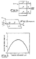
- FIG. 1a is an upper view of a conventional tilted facet laser optical amplifier 15 discussed supra with the indicated angular dimensions serving as a specific example of a general tilted facet amplifier.
- the amplifier 15 has an active layer 16 and input/output optical fibers 17 and 18, respectively, coupled to active layer 16.
- the amplifier has input/output facets which are tilted 7 degrees with respect to the active layer 16, while the input/output optical fibers 17, 18 are tilted at 23 degrees with respect to the facets 19 to achieve optimum coupling in accordance with Snell's law of refraction.
- the graph in Figure 2 indicates that prior art coupling assemblys can achieve a fiber positional sensitivity as little as 1 ⁇ m. However, as noted hereinabove, the prior art is capable of realizing this precision for only one single-mode fiber per package.
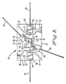
- Figs. 3a and 3b are diagrammatic top and side views respectively of the preferred embodiment of the multi-fiber alignment package for tilted facet optoelectronic components, according to the invention.
- the preferred embodiment is illustrated by a specific example showing the package design for two optical fibers aligned with one tilted facet optoelectronic component. It should be understood that the invention is not limited to this example. More than two optical fibers may be aligned with one component and two or more optical fibers may be aligned with each of two or more components within the package of this invention.
- the embodiment of Figs. 3a and 3b shows the optoelectronic component as a tilted facet optical amplifier. It should be understood that any light emitting and/or light receiving tilted facet component may be used in the practice of the invention. Typically these components will be semiconductor devices.
- the multi-fiber alignment package designated generally by the reference number 20 in the embodiment of Figs. 3a and 3b.
- Package 20 has a carrier 22 serving as a substrate, preferably of one piece to minimize flexing at a joint.
- Carrier 22 is fabricated in the form of a rectangular slab from a thermally conductive material, preferably copper, and has two major surfaces on which the other parts of this package are mounted.
- a submount 24 is secured to the upper major surface of carrier 22. The use of submount 24 facilitates the precise positioning of a tilted facet component to the predetermined offset angle. It also presents a larger surface to carrier 22 for thermal dissipation.
- a tilted facet optoelectronic component 26, is firmly secured to the submount 24.
- Submount 24 is pivoted to the predetermined offset angle computed as explained above, with respect to input and output fibers for purposes of alignment, and is secured to carrier 22 by solder.
- solder Preferably, a high melting point solder is used for this attachment of submount 24 to carrier 22.
- Each optical fiber 30, 31 to be aligned with component 26 is threaded through a fiber-positioning means, preferably a fiber block 28, 29 in which the optical fiber is surrounded with solder to evenly distribute forces on the fibers 30, 31.
- Fibers 30, 31 extend through two opposed sides of fiber blocks 28, 29, the optical fiber end being coupled with the optical component extending outwardly only a short distance to provide stability. The method of securing fiber blocks 28, 29 to carrier 22 and the resulting optoelectronic package will be explained hereinafter.
- Fig. 3a also shows two thermoelectric coolers 32, 33 secured to the underside, or second major surface, of carrier 22.
- Such coolers are known in the art and are commercially available under the trade name "MELCOR” from Materials Electronic Products Corporation, Trenton, New Jersey.
- Each thermoelectric cooler 32, 33 is positioned under one fiber block 28, 29 respectively and each functions to regulate the temperature of carrier 22 in the vicinity of the fiber block with which it is associated.
- the electrical connections of a thermoelectric cooler are known in the art and are not described herein.
- This invention first provides a compensation technique which, when combined with its novel sequential alignment technique, provides a resolution for the tilted facet problem.
- This invention also provides a novel method for the sequential alignment of each optical fiber to a tilted facet component, in which a first optical fiber is aligned with the tilted facet, then secured or "frozen” in position by soldering its fiber block to the carrier and cooling the carrier beneath the area of this fiber connection. With the first fiber thus aligned, and secured in position, a second optical fiber is aligned and secured in position by soldering its fiber block to said carrier without disturbing the alignment of the first fiber connection.
- This sequential process of alignment and soldering utilizes the thermoelectric coolers to regulate the temperature of each fiber connection point and continues until all optical fibers have been aligned and secured.
- a carrier 22 is selected to serve as a thermally conductive substrate.
- the compensating angle at which the tilted facet component must be mounted for optimal coupling to said optical fibers 30, 31 is calculated.
- the tilted facet die 26 may be directly mounted on carrier 22 or preferably on a submount 24 as shown.
- the compensation-tilting is done when the amplifier-submount unit 24 is attached to the carrier 22, prior to the fiber alignment. This submount attachment is typically done with a solder which has a higher melting point compared to the solder used for the fiber alignment, thus preventing the component from shifting during the fiber alignment.
- the tilted facet semiconductor die 26 is mounted on a submount 24 that can be pivoted to a pre-set angle to compensate for the tilted-angle problem, as described above. This permits the optical fiber leads 30, 31 to exit the package at a predetermined angle, usually perpendicular, to the side of the carrier.
- Optical fiber 30 in fiber block 28 is then chosen as the first to be aligned with tilted facet component 26, using an active alignment process. If, for example, component 26 is an optical amplifier, it is electrically biased to operate as a diode laser or light emitting diode.
- Fiber 30 secured within fiber block 28 is then aligned to an optimal coupling position that maximizes its reception of light, a condition monitored by coupling a detector to the opposite end of the fiber 30.
- the manipulation of fiber 30 is achieved by manipulating fiber block 28 with a suction-tipped micromanipulator arm with piezo-electric controls having submicron positional sensitivity.
- connection of fiber block 28 to carrier 22 is made by using a sharp melting point solder such as a pure metal or an alloy eutectic.
- a sharp melting point solder such as a pure metal or an alloy eutectic.
- This type of solder ensures a very narrow temperature range between the liquid phase working temperature of the solder and its solid phase used to hold fiber block 28 in position. By keeping the temperature range narrow, it is possible to maximize the thickness of carrier 22 and its associated structural rigidity despite heat leakage from the hot side to the cold side.
- a typical solder useful for this purpose is Indalloy No. 8, manufactured by Indium Corporation of America, Utica, New York.
- thermoelectric cooler 32 provides its localized cooling to first fiber block 28 connection point in two ways. Cooler 32 first provides cooling by acting as a heat sink since its large face is bonded directly under carrier 22, supplying a large area through which heat can flow away from carrier 22. Secondly, by its nature, thermoelectric cooler 32 provides direct cooling when the voltage polarity on it is reversed. After the optoelectronic package 20 is completed, however, the thermoelectric coolers 32, 33 are used in their normal role of supplying a constant temperature at carrier 22 for proper and stable operation of semiconductor component 26. Carrier 22 and its associated thermoelectric coolers 32, 33 therefore contribute to their own self-assembly.
- thermoelectric cooler 33 is used to provide localized cooling under this second connection.
- Figure 3a shows two thermoelectric coolers 32, 33 secured to carrier 22, which is the heart of the design for stabilizing a two-fiber connection.
- This figure shows the preferred embodiment for a tilted-facet semiconductor optical amplifier 26 which needs two fiber alignments and a tilted submount 24 for the semiconductor 26.
- the amplifier-submount unit 24 By tilting the amplifier-submount unit 24 in this way, the fibers 30, 31 can be precisely aligned with a micromanipulator arm using the same technique for both lasers and tilted-facet components such as amplifiers.
- the entire assembly is mounted on a one-piece carrier 22 to minimize flexing which might happen at a joint.
- the fibers 30, 31 are threaded through blocks 28, 29 which surround them with solder, evenly distributing forces on the fibers.
- carrier 22 may be buttressed with more carrier material 36 at the location of a slot 40 between the fiber blocks, 28, 29 as shown in the top view of Fig. 3b.
- the slot 40 provides some thermal insulation between the separate fiber block connections 28, 29 to impede the lateral transfer of heat.
- thermoelectric coolers 31, 32 under carrier 22 separately regulate the temperature of each fiber connection 28, 29. This allows us to maintain a cold enough temperature at the first fiber connection point 28 to prevent its solder from melting while the second fiber block 29 is connected with solder.
- Figure 4 shows how much temperature difference is developed between each fiber block connection point as a function of carrier thickness for the case where no slot 40 is present. A greater temperature difference is developed when a slot 40 is present because the slot reduces the cross-sectional area through which heat flows.
- This slot can be modified to be a series of small holes of various shapes without altering its purpose.
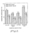
- Figs. 6a-6h illustrate four alternate designs for slot 40 and added carrier material 36.
- Figs 6a-6b show a large slot 80 and a bar 81 of additional carrier material.
- Figs. 6c-d show a series of holes 82 and a bar 83.
- Figs. 6e-f show a slot 84 and a buttress 85.
- Figs. 6g-h show a slot 86 reinforced with carrier material 87.
- Fig. 7 is a graph showing the thermal depression resulting from the configurations of Figs. 6a-6h, from left to right, both with and without cooling from the thermoelectric coolers. The data was obtained from tests of prototype packages.
- Fig. 5 is a diagrammatic top view of a further embodiment of the multi-fiber alignment package for tilted facet optoelectronic components according to the invention.
- package 50 includes a carrier 52, a sub-carrier 54 mounted at a calculated compensation angle, and an optoelectronic integrated circuit 56 secured to subcarrier 54.
- Four fiber blocks 58-61 each have one optical fiber 62-65 respectively threaded therethrough, which fibers are to be coupled to circuit 56.
- Each fiber block has an associated thermoelectric cooler 66-69 secured to the underside of carrier 52 (shown in outline in Fig. 5) and an associated thermistor 70-73.
- the localized cooling technique for sequential alignment of fibers 62-65 and soldering of fiber blocks 66-69 is identical to the previously described method.
- slots as an optional enhancement to the localized cooling technique requires that slots be positioned such that they impede thermal conductivity between any two adjacent fiber block connection positions.
- the layout of Fig. 5 shows seven slots 74-80 to enhance the thermal isolation of the four fiber block connection points.
- Fig. 5 also shows that in some circumstances, it is not possible to couple all optical fibers optimally to a tilted facet component and have them all be perpendicular to the side walls of the package 50.
- this invention can be modified in a number of ways without changing its basic function and operation.
- more than two fibers can be aligned if each had its own thermoelectric cooler and temperature control. Heating and cooling can be supplied by a cold/hot heat exchanger system rather than a thermoelectric cooler.
- the tilted semiconductor component can be on a different type of submount or even no submount, in which case it would be directly bonded to the carrier.
- the carrier material may be metallized ceramic, silicon waferboard, printed circuit board or other material. This system would also work with multimode fiber, GRIN lenses (also commercially available), uptapered fiber, or optical waveguides, provided that these components may be shifted to allow for performing the micromanipulation of an optical alignment.
Landscapes
- Physics & Mathematics (AREA)
- General Physics & Mathematics (AREA)
- Optics & Photonics (AREA)
- Optical Couplings Of Light Guides (AREA)
- Semiconductor Lasers (AREA)
Applications Claiming Priority (2)
| Application Number | Priority Date | Filing Date | Title |
|---|---|---|---|
| US07/400,593 US5026138A (en) | 1989-08-29 | 1989-08-29 | Multi-fiber alignment package for tilted facet optoelectronic components |
| US400593 | 1989-08-29 |
Publications (2)
| Publication Number | Publication Date |
|---|---|
| EP0415094A2 true EP0415094A2 (fr) | 1991-03-06 |
| EP0415094A3 EP0415094A3 (en) | 1991-06-12 |
Family
ID=23584228
Family Applications (1)
| Application Number | Title | Priority Date | Filing Date |
|---|---|---|---|
| EP19900114478 Withdrawn EP0415094A3 (en) | 1989-08-29 | 1990-07-27 | Multi-fiber alignment package for tilted facet optoelectronic components |
Country Status (4)
| Country | Link |
|---|---|
| US (1) | US5026138A (fr) |
| EP (1) | EP0415094A3 (fr) |
| JP (1) | JPH03102305A (fr) |
| CA (1) | CA2022533A1 (fr) |
Cited By (6)
| Publication number | Priority date | Publication date | Assignee | Title |
|---|---|---|---|---|
| WO2001041538A3 (fr) * | 1999-11-15 | 2002-11-14 | Axsun Tech Inc | Procede et systeme de couplage de faisceaux aboutissant dans des systemes optiques de part et d'autre de frontieres hermetiques |
| EP1365488A3 (fr) * | 1998-02-27 | 2004-02-18 | Litton Systems, Inc. | Méthode d'empaquetage d'une assemblage de sous-support |
| CN106094128A (zh) * | 2016-08-29 | 2016-11-09 | 成都全码特时代科技有限公司 | 一种多功能并且内部可调节的光纤夹具装置 |
| CN106154441A (zh) * | 2016-08-29 | 2016-11-23 | 成都全码特时代科技有限公司 | 一种能用于改善通用接口的旁射式光纤刀头 |
| CN106168695A (zh) * | 2016-08-29 | 2016-11-30 | 成都全码特时代科技有限公司 | 一种自动控制打开和关闭状态的光纤夹具装置 |
| CN106199845A (zh) * | 2016-08-29 | 2016-12-07 | 成都全码特时代科技有限公司 | 一种适用于光加工的光纤插头装置 |
Families Citing this family (40)
| Publication number | Priority date | Publication date | Assignee | Title |
|---|---|---|---|---|
| US5282080A (en) * | 1991-12-09 | 1994-01-25 | Sdl, Inc. | Surface coupled optical amplifier |
| US5343548A (en) * | 1992-12-15 | 1994-08-30 | International Business Machines Corporation | Method and apparatus for batch, active alignment of laser arrays to fiber arrays |
| US5434940A (en) * | 1994-03-24 | 1995-07-18 | The Whitaker Corporation | Active fiber needle |
| US6074103A (en) * | 1996-10-15 | 2000-06-13 | Sdl, Inc. | Aligning an optical fiber with electroluminescent semiconductor diodes and other optical components |
| US6137930A (en) * | 1998-07-08 | 2000-10-24 | Optical Switch Corporation | Method and apparatus for aligning optical fibers |
| US6253007B1 (en) | 1998-07-08 | 2001-06-26 | Optical Switch Corporation | Method and apparatus for connecting optical fibers |
| US6236787B1 (en) | 1998-07-08 | 2001-05-22 | Optical Switch Corporation | Method and apparatus for aligning optical fibers using an alignment spacer |
| US6236778B1 (en) | 1998-12-16 | 2001-05-22 | Optical Switch Corporation | Frustrated total internal reflection bus and method of operation |
| US6243511B1 (en) | 1999-02-04 | 2001-06-05 | Optical Switch Corporation | System and method for determining the condition of an optical signal |
| US6597481B1 (en) * | 1999-02-19 | 2003-07-22 | Lucent Technologies Inc. | Controllable wavelength-selective optical cross-connect |
| US6453084B1 (en) | 2000-01-17 | 2002-09-17 | Optical Switch Corporation | System and method for beam-steering using a reference signal feedback |
| US6375365B1 (en) * | 2000-02-28 | 2002-04-23 | Onix Microsystems, Inc. | Apparatus and packaging method to assemble optical modules to a common substrate with adjustable plugs |
| US6567604B1 (en) | 2000-10-25 | 2003-05-20 | Omm, Inc. | Indium plated package for an optical component and process therefore |
| JP2006251703A (ja) * | 2005-03-14 | 2006-09-21 | Denso Corp | 光ファイバセンサ |
| EP1936414A2 (fr) * | 2006-12-14 | 2008-06-25 | JDS Uniphase Corporation | Petit paquet optique doté de multiples éléments soudés optiquement alignés |
| US10386575B2 (en) | 2016-04-01 | 2019-08-20 | Institut National D'optique | Optical assembly and method for coupling a waveguide array to a photonic-integrated circuit |
| US9726830B1 (en) | 2016-06-28 | 2017-08-08 | Senko Advanced Components, Inc. | Connector and adapter system for two-fiber mechanical transfer type ferrule |
| WO2018140981A1 (fr) * | 2017-01-30 | 2018-08-02 | Senko Advanced Components, Inc. | Connecteurs optiques à polarité réversible |
| US10444444B2 (en) | 2017-01-30 | 2019-10-15 | Senko Advanced Components, Inc. | Remote release tab connector assembly |
| US11822133B2 (en) | 2017-07-14 | 2023-11-21 | Senko Advanced Components, Inc. | Ultra-small form factor optical connector and adapter |
| US10718911B2 (en) | 2017-08-24 | 2020-07-21 | Senko Advanced Components, Inc. | Ultra-small form factor optical connectors using a push-pull boot receptacle release |
| US10281669B2 (en) | 2017-07-14 | 2019-05-07 | Senko Advance Components, Inc. | Ultra-small form factor optical connectors |
| US12001064B2 (en) | 2017-07-14 | 2024-06-04 | Senko Advanced Components, Inc. | Small form factor fiber optic connector with multi-purpose boot |
| US11002923B2 (en) | 2017-11-21 | 2021-05-11 | Senko Advanced Components, Inc. | Fiber optic connector with cable boot release having a two-piece clip assembly |
| EP3729153B1 (fr) * | 2017-12-19 | 2024-07-10 | US Conec, Ltd | Mini-connecteur duplex avec mécanisme de polarité poussée-traction et support |
| US11112566B2 (en) | 2018-03-19 | 2021-09-07 | Senko Advanced Components, Inc. | Removal tool for removing a plural of micro optical connectors from an adapter interface |
| MX2020002280A (es) | 2018-03-28 | 2020-10-07 | Senko Advanced Components Inc | Conector de fibra óptica de diseño compacto con un capuchón de múltiples usos. |
| CN112088327A (zh) | 2018-07-15 | 2020-12-15 | 扇港元器件股份有限公司 | 超小型光学连接器和适配器 |
| WO2020036992A1 (fr) | 2018-08-13 | 2020-02-20 | Senko Advanced Components, Inc | Ensemble de tétine d'´etanchéité pour libérer un connecteur de fibre optique d'un réceptacle |
| US10921531B2 (en) | 2018-09-12 | 2021-02-16 | Senko Advanced Components, Inc. | LC type connector with push/pull assembly for releasing connector from a receptacle using a cable boot |
| US10921530B2 (en) | 2018-09-12 | 2021-02-16 | Senko Advanced Components, Inc. | LC type connector with push/pull assembly for releasing connector from a receptacle using a cable boot |
| WO2020055440A1 (fr) | 2018-09-12 | 2020-03-19 | Senko Advanced Componetns, Inc. | Connecteur de type lc avec languette de poussée/traction à clipser pour libérer connecteur d'un réceptacle utilisant une gaine de câble |
| US11806831B2 (en) | 2018-11-21 | 2023-11-07 | Senko Advanced Components, Inc. | Fixture and method for polishing fiber optic connector ferrules |
| US11175464B2 (en) | 2018-11-25 | 2021-11-16 | Senko Advanced Components, Inc. | Open ended spring body for use in an optical fiber connector |
| US12038613B2 (en) | 2019-03-28 | 2024-07-16 | Senko Advanced Components, Inc. | Behind-the-wall optical connector and assembly of the same |
| US11579379B2 (en) | 2019-03-28 | 2023-02-14 | Senko Advanced Components, Inc. | Fiber optic adapter assembly |
| US11340406B2 (en) | 2019-04-19 | 2022-05-24 | Senko Advanced Components, Inc. | Small form factor fiber optic connector with resilient latching mechanism for securing within a hook-less receptacle |
| CN114026480B (zh) | 2019-06-13 | 2023-05-26 | 扇港元器件有限公司 | 用于从插座端口释放光纤连接器的杆驱动闩锁臂和使用方法 |
| US11467354B2 (en) | 2019-07-23 | 2022-10-11 | Senko Advanced Components, Inc. | Ultra-small form factor receptacle for receiving a fiber optic connector opposing a ferrule assembly |
| EP4348321B1 (fr) * | 2021-05-31 | 2024-11-06 | Picadvanced S.A. | Appareil d'hébergement auto-entretenu multifonctionnel et sous-ensemble optique bidirectionnel associé basé sur un circuit intégré photonique |
Family Cites Families (11)
| Publication number | Priority date | Publication date | Assignee | Title |
|---|---|---|---|---|
| US4094579A (en) * | 1976-09-13 | 1978-06-13 | Sperry Rand Corporation | Multimode optical waveguide device with non-normal butt coupling of fiber to electro-optic planar waveguide |
| US4399541A (en) * | 1981-02-17 | 1983-08-16 | Northern Telecom Limited | Light emitting device package having combined heater/cooler |
| JPS57138191A (en) * | 1981-02-19 | 1982-08-26 | Kokusai Denshin Denwa Co Ltd <Kdd> | United structure of semiconductor laser and optical fiber |
| US4854658A (en) * | 1985-10-16 | 1989-08-08 | British Telecommunications Public Limited Company | Radiation deflector assembly |
| US4762386A (en) * | 1986-09-02 | 1988-08-09 | Amp Incorporated | Optical fiber assembly including means utilizing a column load to compensate for thermal effects |
| US4762395A (en) * | 1986-09-02 | 1988-08-09 | Amp Incorporated | Lens assembly for optical coupling with a semiconductor laser |
| US4752109A (en) * | 1986-09-02 | 1988-06-21 | Amp Incorporated | Optoelectronics package for a semiconductor laser |
| US4747657A (en) * | 1987-06-15 | 1988-05-31 | American Telephone And Telegraph Company | Achieving improved radial alignment in an optical package |
| US4769684A (en) * | 1987-07-07 | 1988-09-06 | Rca Inc. | Angle mount header |
| US4871226A (en) * | 1987-10-01 | 1989-10-03 | United Technologies Corporation | Mounting of optical fibers to integrated optical chips |
| DE8816615U1 (de) * | 1988-04-26 | 1990-03-01 | W.C. Heraeus Gmbh, 6450 Hanau | Laser mit einem Multipass-Resonator |
-
1989
- 1989-08-29 US US07/400,593 patent/US5026138A/en not_active Expired - Lifetime
-
1990
- 1990-07-27 EP EP19900114478 patent/EP0415094A3/en not_active Withdrawn
- 1990-08-02 CA CA002022533A patent/CA2022533A1/fr not_active Abandoned
- 1990-08-27 JP JP2222672A patent/JPH03102305A/ja active Pending
Cited By (8)
| Publication number | Priority date | Publication date | Assignee | Title |
|---|---|---|---|---|
| EP1365488A3 (fr) * | 1998-02-27 | 2004-02-18 | Litton Systems, Inc. | Méthode d'empaquetage d'une assemblage de sous-support |
| WO2001041538A3 (fr) * | 1999-11-15 | 2002-11-14 | Axsun Tech Inc | Procede et systeme de couplage de faisceaux aboutissant dans des systemes optiques de part et d'autre de frontieres hermetiques |
| US6554496B1 (en) | 1999-11-15 | 2003-04-29 | Axsun Technologies, Inc. | System and method for coupling beams into optical system across hermetic boundary |
| CN106094128A (zh) * | 2016-08-29 | 2016-11-09 | 成都全码特时代科技有限公司 | 一种多功能并且内部可调节的光纤夹具装置 |
| CN106154441A (zh) * | 2016-08-29 | 2016-11-23 | 成都全码特时代科技有限公司 | 一种能用于改善通用接口的旁射式光纤刀头 |
| CN106168695A (zh) * | 2016-08-29 | 2016-11-30 | 成都全码特时代科技有限公司 | 一种自动控制打开和关闭状态的光纤夹具装置 |
| CN106199845A (zh) * | 2016-08-29 | 2016-12-07 | 成都全码特时代科技有限公司 | 一种适用于光加工的光纤插头装置 |
| CN106154441B (zh) * | 2016-08-29 | 2018-03-30 | 成都全码特时代科技有限公司 | 一种能用于改善通用接口的旁射式光纤刀头 |
Also Published As
| Publication number | Publication date |
|---|---|
| EP0415094A3 (en) | 1991-06-12 |
| JPH03102305A (ja) | 1991-04-26 |
| CA2022533A1 (fr) | 1991-03-01 |
| US5026138A (en) | 1991-06-25 |
Similar Documents
| Publication | Publication Date | Title |
|---|---|---|
| US5026138A (en) | Multi-fiber alignment package for tilted facet optoelectronic components | |
| US7298941B2 (en) | Optical coupling to IC chip | |
| EP1160601B1 (fr) | Module pour diode laser à semiconducteur | |
| US6252726B1 (en) | Dual-enclosure optoelectronic packages | |
| US6712528B2 (en) | Optical bench for an opto-electronic device | |
| EP0466134B1 (fr) | Méthode pour l'alignement passif d'un barreau de laser et de fibres optiques | |
| US4997253A (en) | Electro-optical transducer module and a method of fabricating such a module | |
| GB2293248A (en) | Optical waveguide component coupling using mating substrates | |
| US4944569A (en) | Multi-fiber alignment package for optoelectronic components | |
| JP2002006183A (ja) | 光結合装置 | |
| EP0444610A2 (fr) | Empaquetage d'une fibre optique à mode unique non effilée pour composants optoélectroniques | |
| EP3994777B1 (fr) | Moteur laser supportant de multiples sources laser | |
| US5123067A (en) | Optical head capable of being fitted into a hybrid circuit | |
| US5224184A (en) | Optical multi-chip interconnect | |
| US4957342A (en) | Single-mode optical fiber array package for optoelectronic components | |
| EP0860914B1 (fr) | Module laser à semi-conducteur | |
| EP1271209A1 (fr) | Banc optique pour un dispositif opto-electronique | |
| Lee et al. | Optoelectronic packaging for optical interconnects | |
| US7184646B2 (en) | Optical module with multiple optical sources | |
| Yoon et al. | Compact bidirectional optical module using ceramic blocks | |
| KR200210799Y1 (ko) | 광통신용 레이저 다이오드 모듈 장치 | |
| EP1160600A1 (fr) | Module pour diode laser à semiconducteur | |
| Bo̸rgesen et al. | Packaging of single mode laser diodes | |
| JPH07333471A (ja) | 光モジュール及び光ファイバ固定法 | |
| CZ288941B6 (cs) | Laserový modul |
Legal Events
| Date | Code | Title | Description |
|---|---|---|---|
| PUAI | Public reference made under article 153(3) epc to a published international application that has entered the european phase |
Free format text: ORIGINAL CODE: 0009012 |
|
| AK | Designated contracting states |
Kind code of ref document: A2 Designated state(s): DE FR GB NL |
|
| PUAL | Search report despatched |
Free format text: ORIGINAL CODE: 0009013 |
|
| AK | Designated contracting states |
Kind code of ref document: A3 Designated state(s): DE FR GB NL |
|
| 17P | Request for examination filed |
Effective date: 19910809 |
|
| STAA | Information on the status of an ep patent application or granted ep patent |
Free format text: STATUS: THE APPLICATION HAS BEEN WITHDRAWN |
|
| 18W | Application withdrawn |
Withdrawal date: 19920819 |