EP3994777B1 - Moteur laser supportant de multiples sources laser - Google Patents
Moteur laser supportant de multiples sources laser Download PDFInfo
- Publication number
- EP3994777B1 EP3994777B1 EP20835019.9A EP20835019A EP3994777B1 EP 3994777 B1 EP3994777 B1 EP 3994777B1 EP 20835019 A EP20835019 A EP 20835019A EP 3994777 B1 EP3994777 B1 EP 3994777B1
- Authority
- EP
- European Patent Office
- Prior art keywords
- optical
- reference substrate
- laser source
- array
- laser
- Prior art date
- Legal status (The legal status is an assumption and is not a legal conclusion. Google has not performed a legal analysis and makes no representation as to the accuracy of the status listed.)
- Active
Links
Images


Classifications
-
- H—ELECTRICITY
- H01—ELECTRIC ELEMENTS
- H01S—DEVICES USING THE PROCESS OF LIGHT AMPLIFICATION BY STIMULATED EMISSION OF RADIATION [LASER] TO AMPLIFY OR GENERATE LIGHT; DEVICES USING STIMULATED EMISSION OF ELECTROMAGNETIC RADIATION IN WAVE RANGES OTHER THAN OPTICAL
- H01S5/00—Semiconductor lasers
- H01S5/02—Structural details or components not essential to laser action
- H01S5/022—Mountings; Housings
- H01S5/0235—Method for mounting laser chips
- H01S5/02375—Positioning of the laser chips
- H01S5/0238—Positioning of the laser chips using marks
-
- H—ELECTRICITY
- H01—ELECTRIC ELEMENTS
- H01S—DEVICES USING THE PROCESS OF LIGHT AMPLIFICATION BY STIMULATED EMISSION OF RADIATION [LASER] TO AMPLIFY OR GENERATE LIGHT; DEVICES USING STIMULATED EMISSION OF ELECTROMAGNETIC RADIATION IN WAVE RANGES OTHER THAN OPTICAL
- H01S5/00—Semiconductor lasers
- H01S5/02—Structural details or components not essential to laser action
- H01S5/022—Mountings; Housings
- H01S5/023—Mount members, e.g. sub-mount members
- H01S5/02325—Mechanically integrated components on mount members or optical micro-benches
- H01S5/02326—Arrangements for relative positioning of laser diodes and optical components, e.g. grooves in the mount to fix optical fibres or lenses
-
- H—ELECTRICITY
- H01—ELECTRIC ELEMENTS
- H01S—DEVICES USING THE PROCESS OF LIGHT AMPLIFICATION BY STIMULATED EMISSION OF RADIATION [LASER] TO AMPLIFY OR GENERATE LIGHT; DEVICES USING STIMULATED EMISSION OF ELECTROMAGNETIC RADIATION IN WAVE RANGES OTHER THAN OPTICAL
- H01S5/00—Semiconductor lasers
- H01S5/02—Structural details or components not essential to laser action
- H01S5/022—Mountings; Housings
- H01S5/0225—Out-coupling of light
- H01S5/02251—Out-coupling of light using optical fibres
-
- G—PHYSICS
- G02—OPTICS
- G02B—OPTICAL ELEMENTS, SYSTEMS OR APPARATUS
- G02B6/00—Light guides; Structural details of arrangements comprising light guides and other optical elements, e.g. couplings
- G02B6/24—Coupling light guides
- G02B6/42—Coupling light guides with opto-electronic elements
- G02B6/4201—Packages, e.g. shape, construction, internal or external details
- G02B6/4204—Packages, e.g. shape, construction, internal or external details the coupling comprising intermediate optical elements, e.g. lenses, holograms
- G02B6/4207—Packages, e.g. shape, construction, internal or external details the coupling comprising intermediate optical elements, e.g. lenses, holograms with optical elements reducing the sensitivity to optical feedback
-
- G—PHYSICS
- G02—OPTICS
- G02B—OPTICAL ELEMENTS, SYSTEMS OR APPARATUS
- G02B6/00—Light guides; Structural details of arrangements comprising light guides and other optical elements, e.g. couplings
- G02B6/24—Coupling light guides
- G02B6/42—Coupling light guides with opto-electronic elements
- G02B6/4201—Packages, e.g. shape, construction, internal or external details
- G02B6/4249—Packages, e.g. shape, construction, internal or external details comprising arrays of active devices and fibres
- G02B6/425—Optical features
-
- H—ELECTRICITY
- H01—ELECTRIC ELEMENTS
- H01S—DEVICES USING THE PROCESS OF LIGHT AMPLIFICATION BY STIMULATED EMISSION OF RADIATION [LASER] TO AMPLIFY OR GENERATE LIGHT; DEVICES USING STIMULATED EMISSION OF ELECTROMAGNETIC RADIATION IN WAVE RANGES OTHER THAN OPTICAL
- H01S5/00—Semiconductor lasers
- H01S5/02—Structural details or components not essential to laser action
- H01S5/022—Mountings; Housings
- H01S5/023—Mount members, e.g. sub-mount members
- H01S5/02315—Support members, e.g. bases or carriers
-
- H—ELECTRICITY
- H01—ELECTRIC ELEMENTS
- H01S—DEVICES USING THE PROCESS OF LIGHT AMPLIFICATION BY STIMULATED EMISSION OF RADIATION [LASER] TO AMPLIFY OR GENERATE LIGHT; DEVICES USING STIMULATED EMISSION OF ELECTROMAGNETIC RADIATION IN WAVE RANGES OTHER THAN OPTICAL
- H01S5/00—Semiconductor lasers
- H01S5/02—Structural details or components not essential to laser action
- H01S5/024—Arrangements for thermal management
- H01S5/02469—Passive cooling, e.g. where heat is removed by the housing as a whole or by a heat pipe without any active cooling element like a TEC
-
- H—ELECTRICITY
- H01—ELECTRIC ELEMENTS
- H01S—DEVICES USING THE PROCESS OF LIGHT AMPLIFICATION BY STIMULATED EMISSION OF RADIATION [LASER] TO AMPLIFY OR GENERATE LIGHT; DEVICES USING STIMULATED EMISSION OF ELECTROMAGNETIC RADIATION IN WAVE RANGES OTHER THAN OPTICAL
- H01S5/00—Semiconductor lasers
- H01S5/40—Arrangement of two or more semiconductor lasers, not provided for in groups H01S5/02 - H01S5/30
- H01S5/4025—Array arrangements, e.g. constituted by discrete laser diodes or laser bar
- H01S5/4031—Edge-emitting structures
-
- G—PHYSICS
- G02—OPTICS
- G02B—OPTICAL ELEMENTS, SYSTEMS OR APPARATUS
- G02B6/00—Light guides; Structural details of arrangements comprising light guides and other optical elements, e.g. couplings
- G02B6/24—Coupling light guides
- G02B6/42—Coupling light guides with opto-electronic elements
- G02B6/4201—Packages, e.g. shape, construction, internal or external details
- G02B6/4204—Packages, e.g. shape, construction, internal or external details the coupling comprising intermediate optical elements, e.g. lenses, holograms
-
- G—PHYSICS
- G02—OPTICS
- G02B—OPTICAL ELEMENTS, SYSTEMS OR APPARATUS
- G02B6/00—Light guides; Structural details of arrangements comprising light guides and other optical elements, e.g. couplings
- G02B6/24—Coupling light guides
- G02B6/42—Coupling light guides with opto-electronic elements
- G02B6/4201—Packages, e.g. shape, construction, internal or external details
- G02B6/4219—Mechanical fixtures for holding or positioning the elements relative to each other in the couplings; Alignment methods for the elements, e.g. measuring or observing methods especially used therefor
- G02B6/4228—Passive alignment, i.e. without a detection of the degree of coupling or the position of the elements
- G02B6/423—Passive alignment, i.e. without a detection of the degree of coupling or the position of the elements using guiding surfaces for the alignment
-
- H—ELECTRICITY
- H01—ELECTRIC ELEMENTS
- H01S—DEVICES USING THE PROCESS OF LIGHT AMPLIFICATION BY STIMULATED EMISSION OF RADIATION [LASER] TO AMPLIFY OR GENERATE LIGHT; DEVICES USING STIMULATED EMISSION OF ELECTROMAGNETIC RADIATION IN WAVE RANGES OTHER THAN OPTICAL
- H01S5/00—Semiconductor lasers
- H01S5/005—Optical components external to the laser cavity, specially adapted therefor, e.g. for homogenisation or merging of the beams or for manipulating laser pulses, e.g. pulse shaping
- H01S5/0064—Anti-reflection components, e.g. optical isolators
-
- H—ELECTRICITY
- H01—ELECTRIC ELEMENTS
- H01S—DEVICES USING THE PROCESS OF LIGHT AMPLIFICATION BY STIMULATED EMISSION OF RADIATION [LASER] TO AMPLIFY OR GENERATE LIGHT; DEVICES USING STIMULATED EMISSION OF ELECTROMAGNETIC RADIATION IN WAVE RANGES OTHER THAN OPTICAL
- H01S5/00—Semiconductor lasers
- H01S5/02—Structural details or components not essential to laser action
- H01S5/022—Mountings; Housings
- H01S5/02208—Mountings; Housings characterised by the shape of the housings
-
- H—ELECTRICITY
- H01—ELECTRIC ELEMENTS
- H01S—DEVICES USING THE PROCESS OF LIGHT AMPLIFICATION BY STIMULATED EMISSION OF RADIATION [LASER] TO AMPLIFY OR GENERATE LIGHT; DEVICES USING STIMULATED EMISSION OF ELECTROMAGNETIC RADIATION IN WAVE RANGES OTHER THAN OPTICAL
- H01S5/00—Semiconductor lasers
- H01S5/02—Structural details or components not essential to laser action
- H01S5/024—Arrangements for thermal management
- H01S5/02407—Active cooling, e.g. the laser temperature is controlled by a thermo-electric cooler or water cooling
- H01S5/02415—Active cooling, e.g. the laser temperature is controlled by a thermo-electric cooler or water cooling by using a thermo-electric cooler [TEC], e.g. Peltier element
-
- H—ELECTRICITY
- H01—ELECTRIC ELEMENTS
- H01S—DEVICES USING THE PROCESS OF LIGHT AMPLIFICATION BY STIMULATED EMISSION OF RADIATION [LASER] TO AMPLIFY OR GENERATE LIGHT; DEVICES USING STIMULATED EMISSION OF ELECTROMAGNETIC RADIATION IN WAVE RANGES OTHER THAN OPTICAL
- H01S5/00—Semiconductor lasers
- H01S5/02—Structural details or components not essential to laser action
- H01S5/024—Arrangements for thermal management
- H01S5/02438—Characterized by cooling of elements other than the laser chip, e.g. an optical element being part of an external cavity or a collimating lens
Definitions
- the present invention relates to assemblies for optical communication systems and, more particularly, to a configuration that utilizes a common optical reference substrate to provide coupling between a fiber array and an array of discrete laser diode devices.
- EP 0 642 045 discloses mounting and coupling on a silicon substrate an array of fibers to an array of semiconductor lasers via an array of lenses, the fibers being inserted in V-grooves, the semiconductor lasers being mounted on a further intermediate silicon substrate.
- the present invention relates to assemblies for optical communication systems and, more particularly, to a configuration that utilizes a common optical reference substrate to provide coupling between a fiber array and an array of discrete laser diode devices.
- the assembly may be referred to at times as a "laser engine”, which is intended to refer to the assembled coupling of an array of optical fibers to a set of laser diode sources.
- an optical reference substrate is utilized as a common platform upon which both a fiber array and a laser diode array are disposed and positioned such that alignment between the components is straightforward and efficient.
- a top surface of the optical reference substrate is patterned to include alignment fiducials and bond locations for both the fiber array and the laser diode array.
- a receiving block element of the fiber array may be formed to contain alignment fiducials that mate with the optical reference substrate fiducials and, similarly, a silicon submount for the laser diode array may be configured to contain alignment fiducials that mate with a separate set of alignment fiducials formed on the optical reference substrate.
- Inscribed/etched bond outlines formed on the optical reference substrate may also be used to define the proper locations for both the receiving block element and the silicon submount.
- the receiving block is configured to present the optical fibers at an elevation that allows for straightforward optical alignment with the output beams from the laser diodes positioned on the silicon submount.
- passive optical devices e.g., isolators, lenses, filters, and the like
- Other passive optical devices are also disposed at defined locations on the optical reference substrate, with other fiducials/bond lines formed to delineate the specific locations for placement of these passive devices. It is an aspect of the present invention that the positioning of these passive optical devices on the reference substrate (as opposed to on the silicon submount, as found in many prior art arrangements) simplifies the fabrication and expense of the laser diode source component without compromising the optical alignment created by the passive devices between the laser diode and optical fiber.
- the optical reference substrate may comprise a silicon substrate that is patterned and etched using well-known techniques to create the patterned surface used to properly place and align the receiving block and silicon submount.
- the optical reference substrate may comprise a glass substrate that is similarly processed (perhaps using a machining technique) to create the necessary surface features used for alignment and bonding. Inasmuch as glass does not conduct heat as well as silicon, an opening may be formed through the glass substrate in the location where the laser diode array is located, with an additional heat sink component (for example, a highly conductive metal slug) disposed at this location to direct the thermal energy created by the laser diodes away from the assembly.
- an additional heat sink component for example, a highly conductive metal slug
- thermo-electric cooler may be disposed in combination with the metal slug to "cool" the laser diodes in a well-known manner that maintains operating conditions for the laser devices (where in a preferred arrangement, a non-hermetic TEC may be used).
- TEC thermo-electric cooler
- the use of a low thermal conductivity optical reference substrate ensures that the other components disposed directly on the substrate (i.e., lenses, filters, receiving block) are not affected by the temperature changes at the laser diodes and continue to operate in the nominal ambient of the assembly.
- any other material exhibiting a low thermal conductivity and a coefficient of thermal expansion (CTE) similar to silicon may be used as the optical reference substrate in the arrangement of the present invention.
- An exemplary embodiment of the present invention takes the form of a laser source assembly based upon the use of a common optical reference substrate, with the top major surface of the common optical reference substrate defining an optical reference plane.
- a receiving block (used for supporting an array of optical fibers) is attached to the top major surface of the common optical reference substrate at a first defined location, where the receiving block is formed to include a plurality of V-grooves configured to support the array of optical fibers.
- a silicon submount is also attached to the top major surface of the common optical reference substrate, in this case at a second defined location spaced apart from the first defined location (supporting the fiber receiving block).
- the silicon submount is used to support an array of laser diode sources in optical alignment with the plurality of optical fibers supported by the receiving block in a one-to-one association.
- the laser source assembly will also include a plurality of passive optical devices positioned on the common optical reference substrate between the receiving block and the silicon substrate, the positions of the lenses adjusted to achieve optical alignment between the plurality of laser diode sources and the plurality of optical fibers.
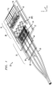
- FIG. 1 is an isometric view of an exemplary laser assembly, including an array of laser diodes and an associated array of optical fibers, positioned in optical alignment on a common optical reference substrate.
- laser assembly will be referred to as a “laser engine”, with the understanding that such an engine consists of a self-contained source of multiple laser beams which are thereafter directed into an associated array of optical fibers.
- an exemplary laser engine 10 is formed in accordance with the principles of the present invention to utilize a common optical reference substrate to support the fiber-related elements of the laser engine in optical alignment with the laser diode-related elements of the same laser engine.
- a common optical reference substrate 12 is used to support a fiber array configuration 14 in optical alignment with a laser diode array source 16.
- FIG. 2 is a cut-away side view of laser engine 10, taken along line 2-2 of FIG. 1 .
- optical reference substrate 12 is formed of a material that exhibits a top reference surface 18 with a degree of flatness sufficient to be used as a defined "reference plane" RP for laser engine 10 (reference plane RP is shown in FIGs. 1 and 2 as the xy plane for the defined three-axis Cartesian system).
- FIGs. 1 and 2 shows an array of four optical fibers 20 as supported within fiber array configuration 14, with an associated array of four semiconductor laser diodes 22 included as part of laser diode array source 16.
- a set of four fiber/laser diode couplings is exemplary only; indeed, a laser engine formed in accordance with the present invention may be used to provide coupling between only a single optical fiber and a single laser diode or, conversely, between a larger array of optical fibers (for example, a "ribbon" of twelve fibers) and associated laser diodes.
- the array of optical fibers 20 may comprise polarization-maintaining (PM) optical fiber, which is often the preferred type of fiber for providing a transmission path from laser diodes.
- PM polarization-maintaining
- the scope of the present invention is not limited to any particularly type of fiber, as along a fiber array configuration 14 is created in a manner that the spacing (pitch) between adjacent fibers is aligned with the set of free-space optical beams emitted from laser diodes 22.
- both fiber array configuration 14 and laser diode array source 16 include support elements that are attached to top reference surface 18 of optical reference substrate 12. By controlling the dimensions of these support elements, the defined reference plane RP of top surface 18 may be translated upward to define the optical axis OA created between fibers 20 and laser diodes 22.
- fiber array configuration 14 is formed to include a receiving block 24 that is attached to top surface 18 of optical reference substrate 12 at a first predetermined location.
- Laser diode array source 16 includes a silicon submount 26 that is also attached to top surface 18 of optical reference substrate 12, as shown in FIGs. 1 and 2 .
- the disposition of these elements on a common reference plane functions to expedite the process steps involved in creating optical alignment between fibers 20 and laser diodes 22.
- laser engine 10 of the present invention is configured to dispose the passive optic components directly on reference top surface 18 of optical reference substrate 12.
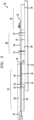
- FIG. 3 is a simplified version of the side view of FIG. 2 , where in this case most of the elements of fiber array configuration 14 have been removed in order to clearly illustrate the placement and dimensions of receiving block 24 and silicon submount 26 on optical reference substrate 12.
- An exemplary optical fiber 20 is shown as positioned within a V-groove 30 formed within receiving block 24, where V-groove 30 prevents the lateral motion of fiber 20, further ensuring continued alignment between the beam emitted from laser diode 22 and associated optical fiber 20.
- passive optics 28 is shown as including lens 32 disposed beyond the output from laser diode 22, with optical isolator 34 positioned between lens 32 and an endface 20E of optical fiber 20.
- the optical axis OA defined by emission from the combination of laser diodes 22 and their associated lenses 24 is used to define the proper dimensions of receiving block 24 so that the core region of optical fiber 20 will also be disposed along optical axis OA.
- the height H of receiving block 24 is designed to facilitate the process of creating optical alignment between fiber 20 and the output beam propagating along optical axis OA.
- alignment with core region 21 of fiber 20 is required to maximize the coupling efficiency between the laser diodes and optical fibers.
- the diameter of optical fiber 20, as well as core region 21, are known parameters, the combination of the depth of V-groove 30 and the height H of receiving block 24 are controlled to achieve this result.
- top surface 18 of optical reference substrate 12 as a reference plane for all components, it is possible to properly configure the plurality of V-grooves 30 formed in receiving block 24 to improve the efficiency of the process used to provide alignment of optical fibers 20 with optical axis OA of laser engine 10.
- an end portion 20E of illustrated fiber 20 extends beyond an endface 24E of receiving block 24, as well as beyond the remaining elements forming fiber array configuration 14. It has been found that the slight protrusion of fiber 20 beyond the endface of fiber array configuration 14 prevents the epoxy bead (used to attach the fibers to the array unit) from wicking upward and covering (in whole or in part) fiber endface 20E. Indeed, as will be discussed below, fiber array configuration 14 is particularly formed to define the axial separation between fiber endface 20E and laser diode 22 (i.e., along the Z-axis direction of laser engine 10.
- FIG. 4 is an isometric view of receiving block 24, showing a set of four V-grooves 30 (shown as V-grooves 30 1 , 30 2 , 30 3 , 30 4 ) formed in parallel within a top surface 36 of receiving block 24. A pitch P between adjacent V-grooves 30 is shown.
- the positioning of lenses 32 may be adjusted, if necessary, to ensure that the individual output beams are directed into the core regions of the supported fibers. In most cases, it is presumed that an array of polarization-maintaining fibers will be supported on receiving block 24.
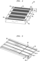
- FIG. 5 illustrates an exemplary fiber support substrate 38, which is one component of fiber array configuration 14.
- Support substrate 38 is shown as including a first plurality of V-grooves 40 that are used to support the stripped end portions of fibers 20, where V-grooves 40 will align with receiving block V-grooves 30 when fiber array configuration 14 is mounted upside-down over receiving block 24 (as best shown in FIGs. 1 and 2 ).
- Also shown in FIG. 5 is a second plurality of V-grooves 42, aligned with first plurality of V-grooves 40 but having a larger depth and width to accommodate a cladded portion of fibers 20 as they are positioned along support substrate 38.
- Substrate 38 is further configured to include a set of vertical slots 44, used to define the placement of an associated cover plate 46, as shown in FIG. 6 .
- FIG. 6 is an isometric view of fiber array configuration 14, showing the positioning of cover plate 46 with respect to substrate 38 and included fibers 20. Also depicted in this view is an endwall surface 45 of cover plate 46.
- the location of vertical slots 44 is used to define the placement of endwall surface 45 of cover plate 46 such that endwall surface 45 will engage with receiving block 24 at the desired position when cover plate 46 is positioned to abut receiving block 24.
- the arrangement of fiber array configuration 14 is used to define the position of fiber array 20 with respect to optical reference substrate 12, which assists in the subsequent procedures used to achieve optical alignment between laser diodes 22 and fibers 20.
- Fiber array configuration 14 is particularly formed to allow for an "overhang" of fiber endface 20E to prevent epoxy or other bonding material associated with the mating of substrate 38 to receiving block 24 from covering the fiber.
- Fiber array configuration 14 is also used to define the optimum position of endface 20E of each fiber 20 such that maximum coupling between laser diodes 22 and fibers 20 is achieved.
- cover plate 46 is used to provide the desired Z-axis positioning of fibers 20 along the optical axis. Referring back to FIG.
- fiber array configuration 14 is disposed in position over receiving block 24 such that endwall surface 45 of cover plate 46 is brought into contact with an endwall surface 25 of receiving block 24.
- this physical "stop" for positioning fiber array configuration 14 thus ensures the desired separation between fibers 20 and laser diodes 22, in accordance with the teachings of the present invention. That is, fiber array configuration includes a mechanical stop that defines the proper axial placement of the fiber endfaces 20E within laser engine 10.
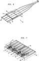
- FIG. 7 is an isometric view of an exemplary silicon submount 26 used to support and energize a set of four semiconductor laser diodes 22, disposed as shown near a front sidewall 26F of silicon submount 26. Also shown in FIG. 7 is a thermistor 50, used to monitor the temperature of silicon submount 26 and a lid 52 disposed as shown. Thermistor 50 is preferably disposed as shown in the middle of the laser diode array.
- a set of metal contact regions 54 is formed on the top surface of submount 26 and are connected to the individual laser diodes 22 by plurality of wirebonds 56. As is well known in the art, an external power source is connected to contact regions 54 and used to energize the individual laser diodes.
- FIG. 8 illustrates laser diode array source 16 (as shown in FIG. 7 ), as well as passive optical devices 28, in position on common optical reference substrate 12.
- the beams generated by laser diodes 22 are shown as passing through an array of lenses 32, where the focused beams formed by lenses 32 thereafter pass through aligned isolators 34.
- common optical reference substrate 12 is formed to include various alignment fiducials and bond locations on its top surface 18 that are used to designate the placement positions for silicon submount 26, lenses 32 and isolators 34 (as well as fiber array receiving block 24).
- FIG. 9 is an isometric view of an exemplary common optical reference substrate 12, particularly showing the various features that are formed in top surface reference plane 18 and used to define the proper positioning and attachment of fiber array configuration 14 and laser diode source 16, as well as passive optical devices 28, so as to form laser engine 10 in accordance with the principles of the present invention.
- FIG. 9 Particularly illustrated in FIG. 9 is a first set of bond lines 72 that are formed in top surface 18 of reference substrate 12 and disposed at a location defined for the placement of receiving block 24.
- An epoxy material is used to bond the components together.
- An epoxy dam 74 may be included with bond lines 72, as shown, to prevent any overflow of epoxy beyond the boundary of receiving block 24.
- receiving block 24 is properly positioned when placed to align with this bond line/dam boundary 76.
- a similar collection of bond lines 78 and epoxy dam 80 is shown in this particular embodiment as formed in top surface 18 of substrate 12 at a spaced-apart location. Bond lines 78 and epoxy dam 80 are formed to support the attachment of silicon submount 26 of laser diode source 16. It is to be understood that the specific topology of bond lines 72, 78 is exemplary only; various other arrangements of trenches (e.g., a set of circles or line segments) may be used.
- a separate plurality of bond lines 82 may be formed and used to support optical isolators 34 in position, with a set of bond pads 84 created for attachment of lenses 32.
- the position of fiber receiving block 24 may be offset with respect to the defined locations of lenses 32 to reduce the coupling of reflections back into laser devices 22.
- optical reference substrate 12 is particularly well-suited for use with an optical reference substrate that is formed of silicon.
- Well-known patterning and etching processes may be used to create the desired shapes at the defined locations, where in one case a deep RIE (DRIE) process may be used.
- DRIE deep RIE
- optical reference substrate 12 may also be formed of a glass (or other material with similar thermal conductivity properties and a CTE match to silicon).
- glass substrate or other material with similar thermal conductivity properties and a CTE match to silicon.
- the following will refer at times to a "glass substrate", with the understanding that other materials having a low thermal conductivity and CTE match to silicon may also be used.
- an alternative substrate configuration may be used for a glass substrate embodiment so as to accommodate the heat generated by laser diodes 22 and direct this heat away from laser diode array source 16 (in particular), as well as laser engine 10 in general.
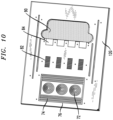
- FIG. 10 illustrates an exemplary glass-based optical reference substrate 12G particularly formed for this purpose.
- glass-based optical reference substrate 12G contains the same/similar bond lines and epoxy dam configuration for receiving block 24 of fiber array structure 14 (as well as features 82, 84 for passive optical devise 28). These features may be formed in top reference surface 18G of glass substrate 12G by using a computer-controlled machining process, or a suitable glass-etching or sand blasting process.
- glass-based optical reference substrate 12G is formed to include a through-opening 90 which exposes a majority of the underside of silicon submount 26.
- FIG. 11 is a view from underneath substrate 12G, showing the location of silicon submount 26 with respect to through-opening 90.
- a separate thermally conductive element may be located in close proximity to silicon submount 26 and create a path for conducting thermal energy away from the operating laser diodes 22.
- various other substrate materials may be substituted for glass that exhibit a similar low thermal conductivity and the use of such a through-opening to create a thermal path is useful with these materials as well.
- FIG. 12 is an isometric view of an exemplary assembly where laser engine 10 is mounted on a printed circuit board (PCB) 92.
- PCB printed circuit board
- FIGs. 13 and 14 illustrate the modifications also made to PCB 92 to accommodate the use of a low thermal conductivity optical reference substrate 12G, as well as a specific set of devices used to conduct heat away from laser diodes 22.
- FIG. 13 is a side view of the assembly, illustrating a through-hole 94 formed in PCB 92 below through-opening 90 formed in optical reference substrate 12G.
- a set of thermal transport elements includes a high thermal conductivity metal block 96 (for example, a copper slug) disposed in direct physical contact with the underside of silicon submount 26 (as best seen in FIG. 14 ).
- TEC 97 this is disposed adjacent to metal block 96 and oriented so that its "cool" surface 97-C is in contact with metal block 96.
- the opposing "hot" surface 97-H of TEC 97 is coupled to a heat sink 98 that is used to dissipate the removed heat in a known fashion.
- a low thermal conductivity optical reference substrate 12G in this embodiment ensures that the reduction of ambient operating temperature provided by TEC 97 to laser diodes 22 is "insulated” from reaching passive optical devices 32, 34, which continue to operate at the nominal ambient temperature. Without providing this type of thermal insulation, the inclusion of a TEC with a laser diode array in this type of laser engine may result in also reducing the ambient temperature of the passive devices, which has been found to result in condensation forming on the optical surfaces (which thus impacts the performance of these devices).
- the TEC used in combination with laser diodes 22 may be disposed (and sealed) within a housing designed as a hermetic enclosure.
- a laser enclosure may be positioned on (and bonded to) silicon submount 26, providing a "window" in a sidewall for allowing the generated beams to exit, but otherwise covering and protecting the individual devices.
- an outer lid 100 may be attached to common optical reference substrate 12 and used to protect the free-space optical signal paths that exist between laser diodes 22 and their associated optical fibers 20.
- Lid 100 is shown as including a pair of sidewalls 110, where bottom terminations 110T of each sidewall 110 is disposed over and bonded to top reference surface 18 of common optical reference substrate 12.
- FIG. 12 illustrates a pair of channel features 112 formed in top surface 18 and used to bond lid 100 to optical reference substrate 12. These same lid attachment channel features 112 are also evident in, for example, FIGs. 9 and 10 .
- each feature includes a pair of parallel epoxy trenches 112 1 , 112 2 , with sidewall 110 disposed to straddle the pair of trenches 112 1 , 112 2 . It is to be understood that various other configurations of lid 100 (including its sidewalls 110) and channel features 112 may be used for attachment to optical reference substrate 12 and are considered as falling within the scope of the present invention.
- FIG. 16 is an isometric view of completely assembled laser engine 10, with FIG. 17 being a side view of the complete assembly.
- the length L of bond lid 100 which is selected to not only protect the free-space optical paths, but also to extend over and encase a portion of fiber array configuration 14 (particularly substrate 38 and receiving block 24). Indeed, it is contemplated that an additional type of sealant, epoxy, or the like may be used to fully secure the complete perimeter.
Landscapes
- Physics & Mathematics (AREA)
- General Physics & Mathematics (AREA)
- Optics & Photonics (AREA)
- Condensed Matter Physics & Semiconductors (AREA)
- Electromagnetism (AREA)
- Optical Couplings Of Light Guides (AREA)
Claims (18)
- Un ensemble de source laser qui comprendun substrat de référence optique commun, une surface principale supérieure du substrat de référence optique commun définissant un plan de référence optique;un bloc de réception fixé à la surface principale supérieure du substrat de référence optique commun à un premier emplacement tel que défini, le bloc de réception comprenant une pluralité de rainures en V configurées pour supporter une pluralité de fibres optiques ;un sous-montage en silicium fixé à la surface principale supérieure du substrat de référence optique commun à un deuxième emplacement défini, à distance du premier emplacement défini, le sous-montage en silicium supportant un réseau de sources de diodes laser en alignement optique avec la pluralité de fibres optiques supportées par le bloc de réception dans une association biunivoque ; etune pluralité de dispositifs optiques passifs fixé à la surface principale supérieure du substrat de référence optique commun et disposé entre le bloc de réception et le substrat de silicium, la pluralité de dispositifs optiques passifs utilisé pour réaliser l'alignement optique entre la pluralité de sources de diodes laser et la pluralité de fibres optiques.
- L'ensemble de source laser tel que défini à la revendication 1, dans lequel le bloc de réception est configuré pour présenter une hauteur H, mesurée à partir du plan de référence optique, associée à la réalisation de l'alignement optique entre une région centrale d'une fibre optique supportée et une diode laser associée du réseau de sources de diodes laser.
- L'ensemble de sources laser tel que défini à la revendication 1, dans lequel l'ensemble comprend en outre
un module de support de réseau de fibres, comprenant un réseau de fibres optiques, le module de support de réseau de fibres comprenant un réseau de rainures en V du module de support et des moyen d'alignement telles que les rainures en V du module de support s'alignent sur les rainures en V du bloc de réception lorsque le module de support de réseau de fibres est disposé sur le bloc de réception et fixé à celui-ci. - L'ensemble de source laser tel que défini à la revendication 3, dans lequel le module de support de réseau de fibres comprend en outre une plaque de recouvrement, dans laquelle une paroi terminale de la plaque de recouvrement est positionnée pour entrer en contact avec une paroi terminale du bloc de réception afin de définir une séparation entre le réseau de fibres optiques et le réseau de sources de diodes laser.
- L'ensemble de source laser tel que défini à la revendication 3, dans lequel le réseau de fibres optiques comprend un réseau de fibres optiques à maintien de polarisation.
- L'ensemble de source laser tel que défini à la revendication 1, dans lequel la surface principale supérieure du substrat de référence optique commun est formée pour inclure des repères d'alignement et des lignes de liaison pour positionner et fixer le bloc de réception au premier emplacement défini et le sous-montage en silicium au deuxième emplacement défini.
- L'ensemble de source laser tel que défini à la revendication 1, dans lequel le substrat de référence optique commun comprend un matériau en silicium.
- L'ensemble de source laser tel que défini à la revendication 7, dans lequel la surface principale supérieure du substrat de référence optique commun est modelée pour définir les emplacements des repères d'alignement et des lignes de liaison, le matériau de silicium étant gravé pour définir les positions de fixation du bloc de réception au premier emplacement défini et du sous-montage en silicium au deuxième emplacement défini.
- L'ensemble de source laser tel que défini à la revendication 1, dans lequel le substrat de référence optique commun comprend un matériau à faible conductivité thermique présentant un CDT similaire au silicium.
- L'ensemble de source laser tel que défini à la revendication 9, dans lequel le substrat de référence optique commun à faible conductivité thermique comprend en outre une ouverture traversante au deuxième emplacement défini, l'ouverture traversante fournissant un passage pour le transfert de chaleur loin du sous-montage en silicium.
- L'ensemble de source laser tel que défini à la revendication 10, dans lequel l'ensemble comprend en outre au moins un élément de transport thermique disposé en contact avec une face inférieure du sous-montage en silicium ouvert dans l'ouverture traversante.
- L'ensemble de source laser tel que défini à la revendication 11, dans lequel l'au moins un élément de transport thermique comprendun bloc métallique à haute conductivité disposé dans le trou traversant et en contact avec le sous-montage en silicium ;un refroidisseur thermoélectrique couplé au bloc métallique à haute conductivité, le refroidisseur thermoélectrique étant utilisé pour réduire davantage la température ambiante du sous-montage en silicium ; etun dissipateur thermique disposé sur le refroidisseur thermoélectrique, dans lequel l'utilisation du substrat de référence optique commun à faible conductivité thermique fournit une isolation thermique entre le sous-montage en silicium et la pluralité de dispositifs optiques passifs disposés sur le substrat de référence optique commun.
- L'ensemble de source laser tel que défini à la revendication 1, dans lequel l'ensemble comprend en outre un composant de couvercle disposé sur une zone définissant un passage optique en espace libre entre le réseau d'appareils à diode laser et la pluralité de fibres optiques.
- La source laser telle que définie à la revendication 13, dans laquelle la surface principale supérieure du substrat de référence optique commun est formée pour inclure des lignes de liaison définissant un emplacement pour le positionnement et la fixation des parois latérales du composant du couvercle.
- La source laser telle que définie à la revendication 1, dans laquelle les composants optiques passifs comprennent une pluralité de lentilles de focalisation fixées à la surface majeure supérieure du substrat optique commun à une position adjacente au sous-montage en silicium.
- La source laser telle que définie à la revendication 15, dans laquelle la surface majeure supérieure du substrat de référence optique commun de référence est traitée pour former une pluralité de plots de collage de lentilles de focalisation à des emplacements utilisés pour fournir un alignement optique entre la pluralité de fibres optiques et la pluralité de diodes laser.
- La source laser telle que définie à la revendication 15, dans laquelle les composants optiques passifs comprennent en outre une pluralité d'isolateurs optiques fixés à la surface majeure supérieure du substrat optique commun à une position située entre la pluralité de lentilles de focalisation et le bloc de réception.
- La source laser telle que définie à la revendication 17, dans laquelle la surface majeure supérieure du substrat de référence optique commun de référence est traitée pour former une pluralité de lignes de liaison à des emplacements définis pour le placement de la pluralité d'isolateurs optiques dans l'alignement optique avec la pluralité de lentilles de couplage.
Applications Claiming Priority (2)
| Application Number | Priority Date | Filing Date | Title |
|---|---|---|---|
| US201962869605P | 2019-07-02 | 2019-07-02 | |
| PCT/US2020/040562 WO2021003306A1 (fr) | 2019-07-02 | 2020-07-01 | Moteur laser supportant de multiples sources laser |
Publications (3)
| Publication Number | Publication Date |
|---|---|
| EP3994777A1 EP3994777A1 (fr) | 2022-05-11 |
| EP3994777A4 EP3994777A4 (fr) | 2023-02-01 |
| EP3994777B1 true EP3994777B1 (fr) | 2024-03-06 |
Family
ID=74101145
Family Applications (1)
| Application Number | Title | Priority Date | Filing Date |
|---|---|---|---|
| EP20835019.9A Active EP3994777B1 (fr) | 2019-07-02 | 2020-07-01 | Moteur laser supportant de multiples sources laser |
Country Status (4)
| Country | Link |
|---|---|
| US (1) | US20220329041A1 (fr) |
| EP (1) | EP3994777B1 (fr) |
| CN (1) | CN114026751A (fr) |
| WO (1) | WO2021003306A1 (fr) |
Families Citing this family (3)
| Publication number | Priority date | Publication date | Assignee | Title |
|---|---|---|---|---|
| CN113050241A (zh) * | 2021-03-31 | 2021-06-29 | 武汉华工正源光子技术有限公司 | 光模块组装方法 |
| US20230176196A1 (en) * | 2021-12-08 | 2023-06-08 | Beijing Voyager Technology Co., Ltd. | Submount for a transmitter of an optical sensing system including a pair of co-packaged laser bars |
| WO2025199923A1 (fr) * | 2024-03-29 | 2025-10-02 | Intel Corporation | Unité de réseau de fibres de verre (fau) à régulation de flux d'époxyde |
Family Cites Families (28)
| Publication number | Priority date | Publication date | Assignee | Title |
|---|---|---|---|---|
| JPH0786693A (ja) * | 1993-09-16 | 1995-03-31 | Toshiba Corp | 光半導体モジュール |
| JP3302458B2 (ja) * | 1993-08-31 | 2002-07-15 | 富士通株式会社 | 集積化光装置及び製造方法 |
| JPH0774343A (ja) * | 1993-08-31 | 1995-03-17 | Fujitsu Ltd | 集積化光装置及びその製造方法 |
| JPH07110420A (ja) * | 1993-10-13 | 1995-04-25 | Mitsubishi Electric Corp | 半導体レーザ素子モジュール,およびその組立方法 |
| JPH07151940A (ja) * | 1993-11-29 | 1995-06-16 | Fujitsu Ltd | 光結合構造とその製造方法 |
| JP3592406B2 (ja) * | 1995-07-10 | 2004-11-24 | 富士通株式会社 | 光モジュール及び光モジュールの製造方法 |
| US5703973A (en) * | 1996-03-29 | 1997-12-30 | Lucent Technologies Inc. | Optical integrated circuit having passively aligned fibers and method using same |
| KR100198460B1 (ko) * | 1996-10-29 | 1999-06-15 | 이계철 | 브이홈에 정렬된 렌즈를 가진 광모듈 및 그 제작방법 |
| US6219470B1 (en) * | 1999-09-23 | 2001-04-17 | Xiang Zheng Tu | Wavelength division multiplexing transmitter and receiver module |
| JP3780769B2 (ja) * | 1999-09-28 | 2006-05-31 | 住友電気工業株式会社 | 光通信装置 |
| US6633599B2 (en) * | 2001-08-01 | 2003-10-14 | Lite Cycles, Inc. | Erbium-doped fiber amplifier pump array |
| US6758610B2 (en) * | 2001-12-10 | 2004-07-06 | Jds Uniphase Corporation | Optical component attachment to optoelectronic packages |
| KR100458250B1 (ko) * | 2002-03-09 | 2004-11-26 | 엘지전자 주식회사 | 마이크로 렌즈를 사용한 레이저 다이오드에 화이버 번들정렬 방법 |
| CN2567837Y (zh) * | 2002-08-05 | 2003-08-20 | 刘胜 | 一种半导体激光发射模块 |
| JP2004233484A (ja) * | 2003-01-29 | 2004-08-19 | Oki Electric Ind Co Ltd | 光モジュール |
| US7422377B2 (en) * | 2003-06-30 | 2008-09-09 | Finisar Corporation | Micro-module with micro-lens |
| EP1517166B1 (fr) * | 2003-09-15 | 2015-10-21 | Nuvotronics, LLC | Boitier de dispositif et procédés de fabrication et d'essai correspondants. |
| KR20050070263A (ko) * | 2003-12-30 | 2005-07-07 | 마이크로솔루션스 주식회사 | 복합형 광소자, 복합형 광소자용 실리콘 광학 벤치,복합형 광소자용 평면형 광도파로 소자, 복합형 광소자의제조방법, 및 이를 위한 광소자의 광축 정렬 방법 |
| JP2005234052A (ja) * | 2004-02-17 | 2005-09-02 | Hamamatsu Photonics Kk | 光送受信モジュール |
| JP4421970B2 (ja) * | 2004-08-02 | 2010-02-24 | パナソニック株式会社 | 光モジュールの製造方法 |
| US7444046B2 (en) * | 2005-10-18 | 2008-10-28 | Nlight Photonics Corporation | Diode laser array coupling optic and system |
| JP4221034B2 (ja) * | 2007-02-26 | 2009-02-12 | 京セラ株式会社 | 光アイソレータ付き偏波保存光ファイバピグテイルおよびこれを用いたレーザーモジュール |
| JP2016004224A (ja) * | 2014-06-19 | 2016-01-12 | 富士通株式会社 | 光学モジュール、光学モジュールの製造方法及び光学装置 |
| US9482818B2 (en) * | 2015-02-23 | 2016-11-01 | Cisco Technology, Inc. | Optically coupling waveguides |
| KR101843469B1 (ko) * | 2016-04-19 | 2018-03-30 | 옵티시스 주식회사 | 광 커넥터 |
| JP6861062B2 (ja) * | 2017-03-22 | 2021-04-21 | 日本ルメンタム株式会社 | サブマウント、光送信モジュール、光モジュール、光伝送装置、並びに、それらの制御方法 |
| US10725254B2 (en) * | 2017-09-20 | 2020-07-28 | Aayuna Inc. | High density opto-electronic interconnection configuration utilizing passive alignment |
| US10734785B2 (en) * | 2018-03-02 | 2020-08-04 | Cisco Technology, Inc. | Silicon photonics co-integrated with quantum dot lasers on silicon |
-
2020
- 2020-07-01 US US17/620,951 patent/US20220329041A1/en active Pending
- 2020-07-01 WO PCT/US2020/040562 patent/WO2021003306A1/fr not_active Ceased
- 2020-07-01 EP EP20835019.9A patent/EP3994777B1/fr active Active
- 2020-07-01 CN CN202080046141.0A patent/CN114026751A/zh active Pending
Also Published As
| Publication number | Publication date |
|---|---|
| WO2021003306A1 (fr) | 2021-01-07 |
| US20220329041A1 (en) | 2022-10-13 |
| EP3994777A4 (fr) | 2023-02-01 |
| EP3994777A1 (fr) | 2022-05-11 |
| CN114026751A (zh) | 2022-02-08 |
Similar Documents
| Publication | Publication Date | Title |
|---|---|---|
| EP1218786B1 (fr) | Boitiers optoelectroniques a gaine duale | |
| US7210859B2 (en) | Optoelectronic components with multi-layer feedthrough structure | |
| US6376268B1 (en) | Optoelectronic assembly and method of making the same | |
| KR101217630B1 (ko) | 광 어셈블리 | |
| US6878875B2 (en) | Small form factor optical transceiver with extended transmission range | |
| US6155724A (en) | Light transmitting module for optical communication and light transmitting unit thereof | |
| KR100921566B1 (ko) | 모듈식 광 트랜시버 | |
| JP2846981B2 (ja) | 光学副集成部品 | |
| EP3994777B1 (fr) | Moteur laser supportant de multiples sources laser | |
| US7066659B2 (en) | Small form factor transceiver with externally modulated laser | |
| EP0415094A2 (fr) | Boîte d'alignement à fibres multiples pour composants opto-électroniques avec des facettes inclinées | |
| CN105705975B (zh) | 用于光学通信设备的方法和系统 | |
| WO2013061742A1 (fr) | Module optique | |
| KR20080087764A (ko) | 광학 어셈블리들 및 이들의 형성 방법들 | |
| WO2017123538A1 (fr) | Dispositif d'alignement de fibres optiques | |
| US6948864B2 (en) | Optoelectronic component with thermoelectric temperature control | |
| US20040129441A1 (en) | Cooled externally modulated laser for transmitter optical subassembly | |
| TWI233509B (en) | Optoelectronic package structure and process for planar passive optical and optoelectronic devices | |
| US4944569A (en) | Multi-fiber alignment package for optoelectronic components | |
| EP1626298A1 (fr) | Boitier optoélectronique et assemblage optique | |
| JP3116900B2 (ja) | 電子冷却器およびこれを用いた光部品モジュール | |
| KR200210799Y1 (ko) | 광통신용 레이저 다이오드 모듈 장치 | |
| WO2005106553A1 (fr) | Module optique a sources optiques multiples | |
| WO2024220284A1 (fr) | Isolation thermique de moteurs laser dans des ensembles d'interconnexion opto-électroniques à haute densité | |
| JPH02115810A (ja) | 光モジュール及びその製造方法 |
Legal Events
| Date | Code | Title | Description |
|---|---|---|---|
| STAA | Information on the status of an ep patent application or granted ep patent |
Free format text: STATUS: THE INTERNATIONAL PUBLICATION HAS BEEN MADE |
|
| PUAI | Public reference made under article 153(3) epc to a published international application that has entered the european phase |
Free format text: ORIGINAL CODE: 0009012 |
|
| STAA | Information on the status of an ep patent application or granted ep patent |
Free format text: STATUS: REQUEST FOR EXAMINATION WAS MADE |
|
| 17P | Request for examination filed |
Effective date: 20211210 |
|
| AK | Designated contracting states |
Kind code of ref document: A1 Designated state(s): AL AT BE BG CH CY CZ DE DK EE ES FI FR GB GR HR HU IE IS IT LI LT LU LV MC MK MT NL NO PL PT RO RS SE SI SK SM TR |
|
| DAV | Request for validation of the european patent (deleted) | ||
| DAX | Request for extension of the european patent (deleted) | ||
| A4 | Supplementary search report drawn up and despatched |
Effective date: 20230105 |
|
| RIC1 | Information provided on ipc code assigned before grant |
Ipc: G02B 6/42 20060101ALI20221223BHEP Ipc: H01S 5/02 20060101ALI20221223BHEP Ipc: H01S 5/022 20210101ALI20221223BHEP Ipc: H01S 5/40 20060101AFI20221223BHEP |
|
| GRAP | Despatch of communication of intention to grant a patent |
Free format text: ORIGINAL CODE: EPIDOSNIGR1 |
|
| STAA | Information on the status of an ep patent application or granted ep patent |
Free format text: STATUS: GRANT OF PATENT IS INTENDED |
|
| INTG | Intention to grant announced |
Effective date: 20230925 |
|
| GRAS | Grant fee paid |
Free format text: ORIGINAL CODE: EPIDOSNIGR3 |
|
| GRAA | (expected) grant |
Free format text: ORIGINAL CODE: 0009210 |
|
| STAA | Information on the status of an ep patent application or granted ep patent |
Free format text: STATUS: THE PATENT HAS BEEN GRANTED |
|
| AK | Designated contracting states |
Kind code of ref document: B1 Designated state(s): AL AT BE BG CH CY CZ DE DK EE ES FI FR GB GR HR HU IE IS IT LI LT LU LV MC MK MT NL NO PL PT RO RS SE SI SK SM TR |
|
| REG | Reference to a national code |
Ref country code: CH Ref legal event code: EP |
|
| REG | Reference to a national code |
Ref country code: DE Ref legal event code: R096 Ref document number: 602020026973 Country of ref document: DE |
|
| REG | Reference to a national code |
Ref country code: IE Ref legal event code: FG4D |
|
| P01 | Opt-out of the competence of the unified patent court (upc) registered |
Effective date: 20240326 |
|
| REG | Reference to a national code |
Ref country code: LT Ref legal event code: MG9D |
|
| PG25 | Lapsed in a contracting state [announced via postgrant information from national office to epo] |
Ref country code: LT Free format text: LAPSE BECAUSE OF FAILURE TO SUBMIT A TRANSLATION OF THE DESCRIPTION OR TO PAY THE FEE WITHIN THE PRESCRIBED TIME-LIMIT Effective date: 20240306 |
|
| REG | Reference to a national code |
Ref country code: NL Ref legal event code: MP Effective date: 20240306 |
|
| PG25 | Lapsed in a contracting state [announced via postgrant information from national office to epo] |
Ref country code: GR Free format text: LAPSE BECAUSE OF FAILURE TO SUBMIT A TRANSLATION OF THE DESCRIPTION OR TO PAY THE FEE WITHIN THE PRESCRIBED TIME-LIMIT Effective date: 20240607 |
|
| PG25 | Lapsed in a contracting state [announced via postgrant information from national office to epo] |
Ref country code: HR Free format text: LAPSE BECAUSE OF FAILURE TO SUBMIT A TRANSLATION OF THE DESCRIPTION OR TO PAY THE FEE WITHIN THE PRESCRIBED TIME-LIMIT Effective date: 20240306 Ref country code: RS Free format text: LAPSE BECAUSE OF FAILURE TO SUBMIT A TRANSLATION OF THE DESCRIPTION OR TO PAY THE FEE WITHIN THE PRESCRIBED TIME-LIMIT Effective date: 20240606 |
|
| PG25 | Lapsed in a contracting state [announced via postgrant information from national office to epo] |
Ref country code: ES Free format text: LAPSE BECAUSE OF FAILURE TO SUBMIT A TRANSLATION OF THE DESCRIPTION OR TO PAY THE FEE WITHIN THE PRESCRIBED TIME-LIMIT Effective date: 20240306 |
|
| PG25 | Lapsed in a contracting state [announced via postgrant information from national office to epo] |
Ref country code: RS Free format text: LAPSE BECAUSE OF FAILURE TO SUBMIT A TRANSLATION OF THE DESCRIPTION OR TO PAY THE FEE WITHIN THE PRESCRIBED TIME-LIMIT Effective date: 20240606 Ref country code: NO Free format text: LAPSE BECAUSE OF FAILURE TO SUBMIT A TRANSLATION OF THE DESCRIPTION OR TO PAY THE FEE WITHIN THE PRESCRIBED TIME-LIMIT Effective date: 20240606 Ref country code: LT Free format text: LAPSE BECAUSE OF FAILURE TO SUBMIT A TRANSLATION OF THE DESCRIPTION OR TO PAY THE FEE WITHIN THE PRESCRIBED TIME-LIMIT Effective date: 20240306 Ref country code: HR Free format text: LAPSE BECAUSE OF FAILURE TO SUBMIT A TRANSLATION OF THE DESCRIPTION OR TO PAY THE FEE WITHIN THE PRESCRIBED TIME-LIMIT Effective date: 20240306 Ref country code: GR Free format text: LAPSE BECAUSE OF FAILURE TO SUBMIT A TRANSLATION OF THE DESCRIPTION OR TO PAY THE FEE WITHIN THE PRESCRIBED TIME-LIMIT Effective date: 20240607 Ref country code: FI Free format text: LAPSE BECAUSE OF FAILURE TO SUBMIT A TRANSLATION OF THE DESCRIPTION OR TO PAY THE FEE WITHIN THE PRESCRIBED TIME-LIMIT Effective date: 20240306 Ref country code: ES Free format text: LAPSE BECAUSE OF FAILURE TO SUBMIT A TRANSLATION OF THE DESCRIPTION OR TO PAY THE FEE WITHIN THE PRESCRIBED TIME-LIMIT Effective date: 20240306 Ref country code: BG Free format text: LAPSE BECAUSE OF FAILURE TO SUBMIT A TRANSLATION OF THE DESCRIPTION OR TO PAY THE FEE WITHIN THE PRESCRIBED TIME-LIMIT Effective date: 20240306 |
|
| REG | Reference to a national code |
Ref country code: AT Ref legal event code: MK05 Ref document number: 1664485 Country of ref document: AT Kind code of ref document: T Effective date: 20240306 |
|
| PG25 | Lapsed in a contracting state [announced via postgrant information from national office to epo] |
Ref country code: SE Free format text: LAPSE BECAUSE OF FAILURE TO SUBMIT A TRANSLATION OF THE DESCRIPTION OR TO PAY THE FEE WITHIN THE PRESCRIBED TIME-LIMIT Effective date: 20240306 Ref country code: LV Free format text: LAPSE BECAUSE OF FAILURE TO SUBMIT A TRANSLATION OF THE DESCRIPTION OR TO PAY THE FEE WITHIN THE PRESCRIBED TIME-LIMIT Effective date: 20240306 |
|
| PG25 | Lapsed in a contracting state [announced via postgrant information from national office to epo] |
Ref country code: NL Free format text: LAPSE BECAUSE OF FAILURE TO SUBMIT A TRANSLATION OF THE DESCRIPTION OR TO PAY THE FEE WITHIN THE PRESCRIBED TIME-LIMIT Effective date: 20240306 |
|
| PG25 | Lapsed in a contracting state [announced via postgrant information from national office to epo] |
Ref country code: NL Free format text: LAPSE BECAUSE OF FAILURE TO SUBMIT A TRANSLATION OF THE DESCRIPTION OR TO PAY THE FEE WITHIN THE PRESCRIBED TIME-LIMIT Effective date: 20240306 |
|
| PG25 | Lapsed in a contracting state [announced via postgrant information from national office to epo] |
Ref country code: IS Free format text: LAPSE BECAUSE OF FAILURE TO SUBMIT A TRANSLATION OF THE DESCRIPTION OR TO PAY THE FEE WITHIN THE PRESCRIBED TIME-LIMIT Effective date: 20240706 |
|
| PG25 | Lapsed in a contracting state [announced via postgrant information from national office to epo] |
Ref country code: SM Free format text: LAPSE BECAUSE OF FAILURE TO SUBMIT A TRANSLATION OF THE DESCRIPTION OR TO PAY THE FEE WITHIN THE PRESCRIBED TIME-LIMIT Effective date: 20240306 Ref country code: PT Free format text: LAPSE BECAUSE OF FAILURE TO SUBMIT A TRANSLATION OF THE DESCRIPTION OR TO PAY THE FEE WITHIN THE PRESCRIBED TIME-LIMIT Effective date: 20240708 |
|
| PG25 | Lapsed in a contracting state [announced via postgrant information from national office to epo] |
Ref country code: CZ Free format text: LAPSE BECAUSE OF FAILURE TO SUBMIT A TRANSLATION OF THE DESCRIPTION OR TO PAY THE FEE WITHIN THE PRESCRIBED TIME-LIMIT Effective date: 20240306 Ref country code: EE Free format text: LAPSE BECAUSE OF FAILURE TO SUBMIT A TRANSLATION OF THE DESCRIPTION OR TO PAY THE FEE WITHIN THE PRESCRIBED TIME-LIMIT Effective date: 20240306 |
|
| PG25 | Lapsed in a contracting state [announced via postgrant information from national office to epo] |
Ref country code: AT Free format text: LAPSE BECAUSE OF FAILURE TO SUBMIT A TRANSLATION OF THE DESCRIPTION OR TO PAY THE FEE WITHIN THE PRESCRIBED TIME-LIMIT Effective date: 20240306 |
|
| PG25 | Lapsed in a contracting state [announced via postgrant information from national office to epo] |
Ref country code: PL Free format text: LAPSE BECAUSE OF FAILURE TO SUBMIT A TRANSLATION OF THE DESCRIPTION OR TO PAY THE FEE WITHIN THE PRESCRIBED TIME-LIMIT Effective date: 20240306 |
|
| PG25 | Lapsed in a contracting state [announced via postgrant information from national office to epo] |
Ref country code: SK Free format text: LAPSE BECAUSE OF FAILURE TO SUBMIT A TRANSLATION OF THE DESCRIPTION OR TO PAY THE FEE WITHIN THE PRESCRIBED TIME-LIMIT Effective date: 20240306 |
|
| PG25 | Lapsed in a contracting state [announced via postgrant information from national office to epo] |
Ref country code: SM Free format text: LAPSE BECAUSE OF FAILURE TO SUBMIT A TRANSLATION OF THE DESCRIPTION OR TO PAY THE FEE WITHIN THE PRESCRIBED TIME-LIMIT Effective date: 20240306 Ref country code: SK Free format text: LAPSE BECAUSE OF FAILURE TO SUBMIT A TRANSLATION OF THE DESCRIPTION OR TO PAY THE FEE WITHIN THE PRESCRIBED TIME-LIMIT Effective date: 20240306 Ref country code: RO Free format text: LAPSE BECAUSE OF FAILURE TO SUBMIT A TRANSLATION OF THE DESCRIPTION OR TO PAY THE FEE WITHIN THE PRESCRIBED TIME-LIMIT Effective date: 20240306 Ref country code: PT Free format text: LAPSE BECAUSE OF FAILURE TO SUBMIT A TRANSLATION OF THE DESCRIPTION OR TO PAY THE FEE WITHIN THE PRESCRIBED TIME-LIMIT Effective date: 20240708 Ref country code: PL Free format text: LAPSE BECAUSE OF FAILURE TO SUBMIT A TRANSLATION OF THE DESCRIPTION OR TO PAY THE FEE WITHIN THE PRESCRIBED TIME-LIMIT Effective date: 20240306 Ref country code: IS Free format text: LAPSE BECAUSE OF FAILURE TO SUBMIT A TRANSLATION OF THE DESCRIPTION OR TO PAY THE FEE WITHIN THE PRESCRIBED TIME-LIMIT Effective date: 20240706 Ref country code: EE Free format text: LAPSE BECAUSE OF FAILURE TO SUBMIT A TRANSLATION OF THE DESCRIPTION OR TO PAY THE FEE WITHIN THE PRESCRIBED TIME-LIMIT Effective date: 20240306 Ref country code: CZ Free format text: LAPSE BECAUSE OF FAILURE TO SUBMIT A TRANSLATION OF THE DESCRIPTION OR TO PAY THE FEE WITHIN THE PRESCRIBED TIME-LIMIT Effective date: 20240306 Ref country code: AT Free format text: LAPSE BECAUSE OF FAILURE TO SUBMIT A TRANSLATION OF THE DESCRIPTION OR TO PAY THE FEE WITHIN THE PRESCRIBED TIME-LIMIT Effective date: 20240306 |
|
| PG25 | Lapsed in a contracting state [announced via postgrant information from national office to epo] |
Ref country code: IT Free format text: LAPSE BECAUSE OF FAILURE TO SUBMIT A TRANSLATION OF THE DESCRIPTION OR TO PAY THE FEE WITHIN THE PRESCRIBED TIME-LIMIT Effective date: 20240306 |
|
| REG | Reference to a national code |
Ref country code: DE Ref legal event code: R097 Ref document number: 602020026973 Country of ref document: DE |
|
| PG25 | Lapsed in a contracting state [announced via postgrant information from national office to epo] |
Ref country code: IT Free format text: LAPSE BECAUSE OF FAILURE TO SUBMIT A TRANSLATION OF THE DESCRIPTION OR TO PAY THE FEE WITHIN THE PRESCRIBED TIME-LIMIT Effective date: 20240306 |
|
| PLBE | No opposition filed within time limit |
Free format text: ORIGINAL CODE: 0009261 |
|
| STAA | Information on the status of an ep patent application or granted ep patent |
Free format text: STATUS: NO OPPOSITION FILED WITHIN TIME LIMIT |
|
| PG25 | Lapsed in a contracting state [announced via postgrant information from national office to epo] |
Ref country code: DK Free format text: LAPSE BECAUSE OF FAILURE TO SUBMIT A TRANSLATION OF THE DESCRIPTION OR TO PAY THE FEE WITHIN THE PRESCRIBED TIME-LIMIT Effective date: 20240306 |
|
| PG25 | Lapsed in a contracting state [announced via postgrant information from national office to epo] |
Ref country code: DK Free format text: LAPSE BECAUSE OF FAILURE TO SUBMIT A TRANSLATION OF THE DESCRIPTION OR TO PAY THE FEE WITHIN THE PRESCRIBED TIME-LIMIT Effective date: 20240306 |
|
| PG25 | Lapsed in a contracting state [announced via postgrant information from national office to epo] |
Ref country code: MC Free format text: LAPSE BECAUSE OF FAILURE TO SUBMIT A TRANSLATION OF THE DESCRIPTION OR TO PAY THE FEE WITHIN THE PRESCRIBED TIME-LIMIT Effective date: 20240306 |
|
| 26N | No opposition filed |
Effective date: 20241209 |
|
| REG | Reference to a national code |
Ref country code: CH Ref legal event code: PL |
|
| PG25 | Lapsed in a contracting state [announced via postgrant information from national office to epo] |
Ref country code: LU Free format text: LAPSE BECAUSE OF NON-PAYMENT OF DUE FEES Effective date: 20240701 |
|
| PG25 | Lapsed in a contracting state [announced via postgrant information from national office to epo] |
Ref country code: LU Free format text: LAPSE BECAUSE OF NON-PAYMENT OF DUE FEES Effective date: 20240701 |
|
| PG25 | Lapsed in a contracting state [announced via postgrant information from national office to epo] |
Ref country code: SI Free format text: LAPSE BECAUSE OF FAILURE TO SUBMIT A TRANSLATION OF THE DESCRIPTION OR TO PAY THE FEE WITHIN THE PRESCRIBED TIME-LIMIT Effective date: 20240306 Ref country code: CH Free format text: LAPSE BECAUSE OF NON-PAYMENT OF DUE FEES Effective date: 20240731 Ref country code: BE Free format text: LAPSE BECAUSE OF NON-PAYMENT OF DUE FEES Effective date: 20240731 |
|
| REG | Reference to a national code |
Ref country code: BE Ref legal event code: MM Effective date: 20240731 |
|
| PGFP | Annual fee paid to national office [announced via postgrant information from national office to epo] |
Ref country code: GB Payment date: 20250612 Year of fee payment: 6 |
|
| PGFP | Annual fee paid to national office [announced via postgrant information from national office to epo] |
Ref country code: FR Payment date: 20250613 Year of fee payment: 6 |
|
| PG25 | Lapsed in a contracting state [announced via postgrant information from national office to epo] |
Ref country code: IE Free format text: LAPSE BECAUSE OF NON-PAYMENT OF DUE FEES Effective date: 20240701 |
|
| PGFP | Annual fee paid to national office [announced via postgrant information from national office to epo] |
Ref country code: DE Payment date: 20250626 Year of fee payment: 6 |
|
| PG25 | Lapsed in a contracting state [announced via postgrant information from national office to epo] |
Ref country code: CY Free format text: LAPSE BECAUSE OF FAILURE TO SUBMIT A TRANSLATION OF THE DESCRIPTION OR TO PAY THE FEE WITHIN THE PRESCRIBED TIME-LIMIT; INVALID AB INITIO Effective date: 20200701 |
|
| PG25 | Lapsed in a contracting state [announced via postgrant information from national office to epo] |
Ref country code: HU Free format text: LAPSE BECAUSE OF FAILURE TO SUBMIT A TRANSLATION OF THE DESCRIPTION OR TO PAY THE FEE WITHIN THE PRESCRIBED TIME-LIMIT; INVALID AB INITIO Effective date: 20200701 |