EP0415439A2 - Dispositif semi-conducteur composÀ© pour détecter un courant excessif - Google Patents
Dispositif semi-conducteur composÀ© pour détecter un courant excessif Download PDFInfo
- Publication number
- EP0415439A2 EP0415439A2 EP90116756A EP90116756A EP0415439A2 EP 0415439 A2 EP0415439 A2 EP 0415439A2 EP 90116756 A EP90116756 A EP 90116756A EP 90116756 A EP90116756 A EP 90116756A EP 0415439 A2 EP0415439 A2 EP 0415439A2
- Authority
- EP
- European Patent Office
- Prior art keywords
- semiconductor device
- conductive layer
- composite semiconductor
- current
- semiconductor element
- Prior art date
- Legal status (The legal status is an assumption and is not a legal conclusion. Google has not performed a legal analysis and makes no representation as to the accuracy of the status listed.)
- Granted
Links
Images


Classifications
-
- G—PHYSICS
- G01—MEASURING; TESTING
- G01R—MEASURING ELECTRIC VARIABLES; MEASURING MAGNETIC VARIABLES
- G01R15/00—Details of measuring arrangements of the types provided for in groups G01R17/00 - G01R29/00, G01R33/00 - G01R33/26 or G01R35/00
- G01R15/14—Adaptations providing voltage or current isolation, e.g. for high-voltage or high-current networks
- G01R15/20—Adaptations providing voltage or current isolation, e.g. for high-voltage or high-current networks using galvano-magnetic devices, e.g. Hall-effect devices, i.e. measuring a magnetic field via the interaction between a current and a magnetic field, e.g. magneto resistive or Hall effect devices
- G01R15/202—Adaptations providing voltage or current isolation, e.g. for high-voltage or high-current networks using galvano-magnetic devices, e.g. Hall-effect devices, i.e. measuring a magnetic field via the interaction between a current and a magnetic field, e.g. magneto resistive or Hall effect devices using Hall-effect devices
-
- G—PHYSICS
- G01—MEASURING; TESTING
- G01R—MEASURING ELECTRIC VARIABLES; MEASURING MAGNETIC VARIABLES
- G01R31/00—Arrangements for testing electric properties; Arrangements for locating electric faults; Arrangements for electrical testing characterised by what is being tested not provided for elsewhere
- G01R31/26—Testing of individual semiconductor devices
- G01R31/2644—Adaptations of individual semiconductor devices to facilitate the testing thereof
-
- G—PHYSICS
- G01—MEASURING; TESTING
- G01R—MEASURING ELECTRIC VARIABLES; MEASURING MAGNETIC VARIABLES
- G01R31/00—Arrangements for testing electric properties; Arrangements for locating electric faults; Arrangements for electrical testing characterised by what is being tested not provided for elsewhere
- G01R31/28—Testing of electronic circuits, e.g. by signal tracer
- G01R31/30—Marginal testing, e.g. by varying supply voltage
- G01R31/3004—Current or voltage test
Definitions
- the present invention relates to a semiconductor device including semiconductor elements such as diodes, transistors, and thyristors, and more particularly, to a composite semiconductor device having a function for overcurrent detection.
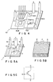
- Fig. 5A is a perspective view (resin-sealed portion is omitted) showing an internal structure of the IGBT
- Fig. 5B is a view showing an appearance of the IGBT
- Fig. 5C is a view showing an equivalent circuit, respectively.
- an insulating substrate 1 is used, which includes conductive layers 2, 3, and 4 such as copper foils provided on a ceramic substrate.
- a semiconductor element chip (IGBT) 5 has a collector electrode (main electrode) on one major surface (lower surface) and an emitter electrode (main electrode) 6 and a gate electrode 7 on the other major surface (upper surface).
- the collector electrode of the semiconductor element 5 is mounted on the conductive layer 2 by soldering or the like, and the conductive layers 3 and 4 are electrically connected to the gate electrode 7 and the emitter electrode 6 through a metal wire or the like, respectively.
- the conductive layers 2, 3, and 4 are connected to external terminals 8, 9, and 10 of a collector (C), a gate (G), and an emitter (E), respectively.
- the semiconductor element described above is finally resin-molded and has an appearance shown in Fig. 5B.
- a resistor 11 for detecting a current is connected in series with the main current path as shown in Fig. 6A, or a current transformer 12 is connected to the main current line as shown in Fig. 6B, thereby performing a current detection.
- Information for the overcurrent passage is then obtained from the current detection. The information is fed from T1 and T2 terminals or T3 and T4 terminals, and is fed back to a drive circuit of the semiconductor device to reduce the overcurrent.
- the current detector such as current transformers, resistors, etc.
- a current transformer must be added to the high power semiconductor device in the case where the current is high, and a resistor must be also added to the high power semiconductor device in the case of a comparatively low current.
- the handling of the resistor or current transformer is very complicated.
- the function for current detection has the above-described inconvenience.
- FIG. 7A A generally used composite semiconductor device having a function for overcurrent detection is shown in Fig. 7A.
- FIG. 7A The same reference numerals in Fig. 7A denote the same or corresponding parts as in Figs. 5A to 5C.
- a semiconductor element 25 shown in Fig. 7A has a current detection electrode 26 which is connected to an external terminal 28 for current detection (Es) through both a metal wire and a conductive layer 27.
- Es current detection
- Fig. 7B shows an equivalent circuit of the composite semiconductor device.
- the detected output appears between the current detection external terminal 28 (or Es) and an emitter external terminal 10 (or E). Therefore, when a plurality of semiconductor elements connected in series with one another are used (usual inverters for three-phase motor drive or the like), electric potentials of ground terminals (emitter E) for current detection outputs in semiconductor elements are different from one another, so that the design of the feedback circuit is undesirably complicated.
- a semiconductor element must be newly designed and developed.
- the area of the active region is decreased due to the electrode area provided for the current detection output.
- the chip size of the semiconductor element becomes large to increase the chip cost.
- an object of the present invention to provide a composite semiconductor device which includes a current detection means having low power loss and excellent detection characteristics.
- a semiconductor element through which a main current (load current) flows and a magnetoelectric transducer for detecting a magnetic field produced by the main current are integrally provided on an insulating substrate having a conductive layer for effectively producing the magnetic field.
- the main electrode of the semiconductor element is an electrode through which a controlled load current flows.
- anode and cathode electrodes are main electrodes.
- collector and emitter electrodes are main electrodes, and drain and source electrodes are main electrodes in a MOSFET or the like.
- a conductive layer for connecting the main electrode of the semiconductor element to the main current external terminal constitutes a current path for a main current.
- a magnetic field proportional to the magnitude of the main current is produced around the conductive layer.
- the magnetic field is detected using a magnetoelectric transducer, such as Hall effect elements, magnetoresistance elements, etc., which converts a magnetic signal to an electrical signal. That is, the magnetic field strength proportional to the magnitude of the main current is converted into the electrical signal by the magnetoelectric transducer, and this electrical signal appears across a pair of signal output terminals of the transducer.
- the conductive layer has a U-shaped portion which centers the magnetic flux corresponding to the main current, and the magnetoelectric transducer is located at the center of the U-shaped conductive layer.
- the electrical signal fed from the magnetoelectric transducer is fed back to the drive circuit of the semiconductor device.
- the detected electrical signal from the magnetoelectric transducer is fed back to the drive circuit, thereby suppressing an increase in the main current or breaking the main current. Therefore, unwanted breakdown of the semiconductor device can be prevented.
- a chip-like IGBT 102 is used as a semiconductor element through which a main current flows.
- the IGBT 102 is mounted on an insulating substrate 101 which includes a conductive layer 103 provided on a ceramic substrate made of, e.g., alumina or aluminum nitride.
- the lower surface of the IGBT is a collector electrode and soldered on the conductive layer 103.
- a collector external terminal 104 is soldered on the conductive layer 103.
- a gate electrode 105 and an emitter electrode 106 serving as a main electrode are provided on the upper surface of the semiconductor element 102, and a metal wire is bonded on these electrodes by ultrasonic bonding or the like and connected to conductive layers 107 and 108, respectively.
- a gate external terminal 109 and an emitter external terminal 110 are soldered on the conductive layers 107 and 108, respectively.
- the conductive layer 108 is patterned so as to provide a U-shaped configuration as shown in Fig. IA, and a Hall sensor 111 of a magnetoelectric transducer is fixed on an insulator of the substrate 101 located inside the U-shaped portion.
- the Hall sensor 111 comprises a pair of control current input leads and a pair of Hall voltage output leads.
- the pair of control current input leads are connected to conductive layers 112 and 113, and control current input external terminals 116 and 117 are soldered on the conductive layers 112 and 113, respectively.
- the pair of Hall voltage output leads are connected to conductive layers 114 and 115, and Hall voltage output external terminals, i.e., current detection signal output external terminals 118 and 119 are soldered on the conductive layers 114 and 115.
- the substrate is resin-molded except a part of each external terminal to obtain a composite semiconductor device.
- the conductive layer for connecting the main electrode of the semiconductor element to the main current external terminal the metal wire and the conductive layer 108 are used in the emitter, and the conductive layer 103 is used in the collector.
- a magnetic field indicated by a broken line 121 is produced around the conductive layer 108 according to the Ampere's corkscrew rule. Since the conductive layer 108 has the U-shaped configuration, a magnetic flux passing vertically through the substrate surface is concentrated inside the U-shaped portion. A mark X in Fig. 1B shows that a magnetic flux B is directed from the upper surface to the lower surface of the drawing.
- the Hall sensor is arranged inside the U-shaped portion which has a high magnetic flux density, and a voltage proportional to the magnetic field, i.e., to the magnitude of the main current flowing between the collector and the emitter is provided between the Hall voltage output external terminals 118 and 119. Note that a control current with several mA is supplied between the control current input external terminals 116 and 117 of the Hall sensor.
- the composite semiconductor device since the current flowing through the semiconductor element is detected in the composite semiconductor device, a resistor, a current transformer, or the like specially provided for current detection need not be added to the semiconductor device. Therefore, the composite semiconductor device can be easily handled.
- the magnetic field which is produced by the main current flowing through the conductive layer of the semiconductor element, is effectively employed to perform the current detection, the power loss due to the current detection does not almost occur.
- the current detection can be performed in an operation of the semiconductor element at all frequency bands including a DC current, and the current detection signal output terminals are electrically insulated from the electrodes of the semiconductor element. For this reason, the feedback circuit or the like can be easily designed.
- the main current is detected from the magnetic field produced from the emitter conductive layer of the semiconductor element
- the current may be detected from a conductive layer of the collector side in the same manner as described above according to the second embodiment, as shown in Fig. 2.
- the collector electrode of the lower surface of the semiconductor element 102 is fixed by soldering or the like on a conductive layer 203 which includes a U-shaped portion 208.
- a magnetoelectric transducer 211 is arranged inside the U-shaped portion.
- the main current may be detected by a sum of magnetic fields produced from a conductive layer of the emitter side and from a conductive layer of the collector side.
- a magnetoelectric transducer is arranged inside a U-shaped portion surrounded by a part 304 of a conductive layer 303 of a collector side and a conductive layer 308 of an emitter side.
- the magnetoelectric transducer is not shown, it is desired to provide an interlevel insulator at an intersection between input/output leads of the transducer and a conductive layer.
- the conductive layer may be circular and a swirl coil may be formed by the conductive layer.
- a parasitic reactance which cannot be negligible is added to the main current path in accordance with an increase in the number of turns of the coil, switching characteristics may be lowered. Therefore, the increase in the number of turns must be carefully determined.
- the magnetic field produced by the conductive layer is used, a magnetic field produced from a part of the external terminal or the metal wire through which the main current flows may be employed.
- the Hall sensor must be properly located.
- the Hall sensor is used as the magnetoelectric transducer for current detection
- a Hall IC with an amplifier may be used. In this case, a relatively low current can be detected with a high sensitivity.
- a magnetoresistance element or the like may be used. In this case, although the linearity of the output signal of the magnetoelectric transducer is lowered with respect to the main current of the semiconductor element no problem is caused as long as the main current and the output signal have a one-to-one correspondence.
- the IGBT is used as the semiconductor element, another high power semiconductor elements may be employed.
- a plurality of semiconductor elements such as free-wheeling diodes may be included in the composite semiconductor device.
- This embodiment is shown in Fig. 4.
- reference numeral 408 denotes a conductive layer for producing a magnetic field
- reference numeral 320 denotes a free-wheeling diode. In this case, when an inductive load is connected, a magnetic field produced by a current flowing through the diode is not detected by the Hall sensor.
- the semiconductor device according to the present invention will include so-called power modules which contain a plurality of power devices arranged in one package together with another electric parts, and will also involve resin-molded semiconductor structures which includes a power device using a lead frame as a substrate, and a magnetoelectric element.
- the semiconductor element is not limited to it.
- resin-molded semiconductor devices with exposed outer leads may be used.
- the magnetic field produced by the current flowing through the conductive layer in the device is detected by the incorporated magnetoelectric transducer, and the overcurrent control can be performed by the detected signal output of the transducer. Therefore, according to the device of the present invention, externally adding parts for current detection such as resistors, current transformers, etc., will not be required, and the magnetic field produced by the main current can be effectively utilized. Therefore, the power loss due to the current detection will be extremely low, and detected characteristics will be excellent at all frequency bands including DC current.
- detected signal output terminals are electrically insulated from electrode terminals of the semiconductor element, output terminals of the devices for current detection will be commonly grounded when a plurality of semiconductor devices are used to be connected in series with one another thereby facilitating the design of the feedback circuit.
Landscapes
- Physics & Mathematics (AREA)
- General Physics & Mathematics (AREA)
- Engineering & Computer Science (AREA)
- General Engineering & Computer Science (AREA)
- Hall/Mr Elements (AREA)
- Inverter Devices (AREA)
- Measuring Magnetic Variables (AREA)
- Power Conversion In General (AREA)
- Measurement Of Current Or Voltage (AREA)
- Testing Of Individual Semiconductor Devices (AREA)
- Measuring Instrument Details And Bridges, And Automatic Balancing Devices (AREA)
Applications Claiming Priority (2)
| Application Number | Priority Date | Filing Date | Title |
|---|---|---|---|
| JP227245/89 | 1989-09-01 | ||
| JP1227245A JPH0390872A (ja) | 1989-09-01 | 1989-09-01 | 半導体装置 |
Publications (3)
| Publication Number | Publication Date |
|---|---|
| EP0415439A2 true EP0415439A2 (fr) | 1991-03-06 |
| EP0415439A3 EP0415439A3 (en) | 1992-03-04 |
| EP0415439B1 EP0415439B1 (fr) | 1996-07-17 |
Family
ID=16857794
Family Applications (1)
| Application Number | Title | Priority Date | Filing Date |
|---|---|---|---|
| EP19900116756 Expired - Lifetime EP0415439B1 (fr) | 1989-09-01 | 1990-08-31 | Dispositif semi-conducteur composé pour détecter un courant excessif |
Country Status (5)
| Country | Link |
|---|---|
| US (1) | US5023684A (fr) |
| EP (1) | EP0415439B1 (fr) |
| JP (1) | JPH0390872A (fr) |
| KR (1) | KR930011798B1 (fr) |
| DE (1) | DE69027821T2 (fr) |
Cited By (9)
| Publication number | Priority date | Publication date | Assignee | Title |
|---|---|---|---|---|
| EP0596584A3 (fr) * | 1992-11-04 | 1995-03-15 | Eac Automation Consult Gmbh | Arrangement de saisie de perturbation. |
| WO1995025959A1 (fr) * | 1994-03-24 | 1995-09-28 | Robert Bosch Gmbh | Appareil de mesure de l'intensite de courant |
| WO1999060416A1 (fr) * | 1998-05-14 | 1999-11-25 | Daimlerchrysler Ag | Procede de mesure sans contact d'un courant traversant un conducteur a l'aide d'un detecteur de hall et systeme de detection de hall approprie |
| DE19959003A1 (de) * | 1999-12-08 | 2001-06-13 | Abb Research Ltd | Elektronischer Schalter mit Überstrom-Schutzvorrichtung |
| WO2002082109A1 (fr) | 2001-04-09 | 2002-10-17 | Koninklijke Philips Electronics N.V. | Circuit integre avec interface de test d'alimentation |
| EP1111693A3 (fr) * | 1999-12-20 | 2004-10-13 | Sanken Electric Co., Ltd. | Détecteur de courant élevé avect un dispositif à effet Hall |
| DE202006013311U1 (de) * | 2006-08-30 | 2008-01-03 | Merten Gmbh & Co. Kg | Anschlusseinheit eines Bussystems |
| US7375507B2 (en) | 2005-10-08 | 2008-05-20 | Melexis Technologies Sa | Assembly group for current measurement |
| CN103022976A (zh) * | 2012-12-13 | 2013-04-03 | 广州三晶电气有限公司 | 一种变频器输出短路保护电路及保护方法 |
Families Citing this family (30)
| Publication number | Priority date | Publication date | Assignee | Title |
|---|---|---|---|---|
| US5216405A (en) * | 1991-01-14 | 1993-06-01 | General Motors Corporation | Package for the magnetic field sensitive device |
| US5170312A (en) * | 1991-11-04 | 1992-12-08 | Motorola, Inc. | Protection circuit on a lead of a power device |
| US5332973A (en) * | 1992-05-01 | 1994-07-26 | The University Of Manitoba | Built-in fault testing of integrated circuits |
| JPH07191114A (ja) * | 1993-12-27 | 1995-07-28 | Chodendo Sensor Kenkyusho:Kk | Squid用キャリヤ |
| JPH09322559A (ja) * | 1996-05-31 | 1997-12-12 | Aisin Aw Co Ltd | モータ駆動装置 |
| US5990533A (en) * | 1997-03-31 | 1999-11-23 | Nec Corporation | Semiconductor device including a magnetoresistance effect element functioning as a current detector |
| DE19739923C2 (de) * | 1997-09-11 | 2002-02-28 | Fraunhofer Ges Forschung | Verfahren und Vorrichtung zur gepulsten Hochstrombelastung integrierter Schaltungen und Strukturen |
| US6102210A (en) * | 1997-10-27 | 2000-08-15 | Sumitomo Bakelite Company Limited | Carrier tape for electronic components |
| US6094330A (en) * | 1998-01-14 | 2000-07-25 | General Electric Company | Circuit interrupter having improved current sensing apparatus |
| US5933306A (en) * | 1998-01-14 | 1999-08-03 | General Electric Company | Circuit breaker with ground fault detection module |
| US6141197A (en) * | 1998-03-10 | 2000-10-31 | General Electric Company | Smart residential circuit breaker |
| US6225684B1 (en) * | 2000-02-29 | 2001-05-01 | Texas Instruments Tucson Corporation | Low temperature coefficient leadframe |
| KR100390013B1 (ko) * | 2000-10-05 | 2003-07-04 | 한국원자력연구소 | 핵연료봉 지지체 부착을 위한 레이저용접 장치 |
| JP2003009508A (ja) * | 2001-06-19 | 2003-01-10 | Mitsubishi Electric Corp | 電力用半導体装置 |
| WO2003085814A1 (fr) * | 2002-04-04 | 2003-10-16 | Hitachi, Ltd. | Convertisseur de puissance, systeme d'alimentation equipe de celui-ci et corps mobile |
| US7199435B2 (en) * | 2002-10-09 | 2007-04-03 | Fairchild Semiconductor Corporation | Semiconductor devices containing on-chip current sensor and methods for making such devices |
| JP4387119B2 (ja) * | 2003-03-27 | 2009-12-16 | 三菱電機株式会社 | 半導体装置 |
| DE10333089B4 (de) * | 2003-07-21 | 2016-12-29 | Infineon Technologies Ag | Stromauswertevorrichtung und Verfahren zum Herstellen derselben |
| JP2007121239A (ja) * | 2005-10-31 | 2007-05-17 | Denso Corp | 電流センサ及びその製造方法 |
| US8324721B2 (en) * | 2008-07-01 | 2012-12-04 | Texas Instruments Incorporated | Integrated shunt resistor with external contact in a semiconductor package |
| US7847391B2 (en) * | 2008-07-01 | 2010-12-07 | Texas Instruments Incorporated | Manufacturing method for integrating a shunt resistor into a semiconductor package |
| KR101116172B1 (ko) * | 2008-12-09 | 2012-03-06 | 주식회사 흙살림 | 친환경 새싹채소 재배용 키트 및 그를 이용한 새싹채소 재배방법 |
| JP2011188123A (ja) * | 2010-03-05 | 2011-09-22 | Panasonic Corp | ポーラ変調方式を用いた送信回路及び通信機器 |
| JP5794777B2 (ja) | 2010-12-22 | 2015-10-14 | 三菱電機株式会社 | 半導体装置 |
| US8969985B2 (en) | 2011-08-30 | 2015-03-03 | Infineon Technologies Ag | Semiconductor chip package and method |
| DE102012210261B4 (de) * | 2012-06-19 | 2019-03-28 | Semikron Elektronik Gmbh & Co. Kg | Leistungshalbleitermodul und Verfahren zum Betrieb eines Leistungshalbleitermoduls |
| US9482700B2 (en) * | 2013-01-20 | 2016-11-01 | Lenovo Enterprise Solutions (Singapore) Pte. Ltd. | Current detector to sense current without being in series with conductor |
| EP3032268B1 (fr) * | 2014-12-09 | 2018-03-28 | Rohm Co., Ltd. | Circuit intégré avec un capteur de Hall sur puce |
| US9564423B2 (en) | 2015-06-23 | 2017-02-07 | Infineon Technologies Ag | Power package with integrated magnetic field sensor |
| IT201900016193A1 (it) | 2019-09-12 | 2021-03-12 | St Microelectronics Srl | Dispositivo di potenza, sistema includente il dispositivo di potenza, metodo di fabbricazione del dispositivo di potenza e metodo di controllo del dispositivo di potenza |
Family Cites Families (10)
| Publication number | Priority date | Publication date | Assignee | Title |
|---|---|---|---|---|
| FR2484171A1 (fr) * | 1980-06-04 | 1981-12-11 | Commissariat Energie Atomique | Amplificateur lineaire hybride ultra-rapide |
| JPS58151814A (ja) * | 1982-03-04 | 1983-09-09 | 株式会社東芝 | 過電流保護回路付きhスイツチ回路 |
| JPS5933894A (ja) * | 1982-08-19 | 1984-02-23 | 電気化学工業株式会社 | 混成集積用回路基板の製造法 |
| JPS6197574A (ja) * | 1984-10-19 | 1986-05-16 | Nissan Motor Co Ltd | 半導体電流検出装置 |
| JPH0648165B2 (ja) * | 1985-02-13 | 1994-06-22 | 株式会社三協精機製作所 | 磁気抵抗効果型素子 |
| CH669068A5 (de) * | 1986-04-29 | 1989-02-15 | Landis & Gyr Ag | Integrierbares hallelement. |
| US4816984A (en) * | 1987-02-06 | 1989-03-28 | Siemens Aktiengesellschaft | Bridge arm with transistors and recovery diodes |
| DE3854457T2 (de) * | 1987-07-07 | 1996-02-29 | Nippon Denso Co | Stromdetektoranordnung mit ferromagnetischem Magnetwiderstandselement. |
| CH674089A5 (fr) * | 1987-10-16 | 1990-04-30 | Lem Liaisons Electron Mec | |
| US4945445A (en) * | 1988-09-29 | 1990-07-31 | Gentron Corporation | Current sense circuit |
-
1989
- 1989-09-01 JP JP1227245A patent/JPH0390872A/ja active Pending
-
1990
- 1990-08-31 US US07/575,614 patent/US5023684A/en not_active Expired - Lifetime
- 1990-08-31 DE DE69027821T patent/DE69027821T2/de not_active Expired - Fee Related
- 1990-08-31 KR KR1019900013628A patent/KR930011798B1/ko not_active Expired - Lifetime
- 1990-08-31 EP EP19900116756 patent/EP0415439B1/fr not_active Expired - Lifetime
Cited By (13)
| Publication number | Priority date | Publication date | Assignee | Title |
|---|---|---|---|---|
| EP0596584A3 (fr) * | 1992-11-04 | 1995-03-15 | Eac Automation Consult Gmbh | Arrangement de saisie de perturbation. |
| WO1995025959A1 (fr) * | 1994-03-24 | 1995-09-28 | Robert Bosch Gmbh | Appareil de mesure de l'intensite de courant |
| WO1999060416A1 (fr) * | 1998-05-14 | 1999-11-25 | Daimlerchrysler Ag | Procede de mesure sans contact d'un courant traversant un conducteur a l'aide d'un detecteur de hall et systeme de detection de hall approprie |
| DE19959003A1 (de) * | 1999-12-08 | 2001-06-13 | Abb Research Ltd | Elektronischer Schalter mit Überstrom-Schutzvorrichtung |
| EP1111693A3 (fr) * | 1999-12-20 | 2004-10-13 | Sanken Electric Co., Ltd. | Détecteur de courant élevé avect un dispositif à effet Hall |
| US6812690B2 (en) | 2001-04-09 | 2004-11-02 | Koninklijke Philips Electronics N.V. | Integrated circuit with power supply test interface |
| WO2002082109A1 (fr) | 2001-04-09 | 2002-10-17 | Koninklijke Philips Electronics N.V. | Circuit integre avec interface de test d'alimentation |
| CN1314975C (zh) * | 2001-04-09 | 2007-05-09 | 皇家菲利浦电子有限公司 | 有电源测试接口的集成电路 |
| KR100967727B1 (ko) * | 2001-04-09 | 2010-07-05 | 엔엑스피 비 브이 | 전류 공급 테스트 인터페이스를 구비하는 집적 회로 어셈블리 |
| US7375507B2 (en) | 2005-10-08 | 2008-05-20 | Melexis Technologies Sa | Assembly group for current measurement |
| DE202006013311U1 (de) * | 2006-08-30 | 2008-01-03 | Merten Gmbh & Co. Kg | Anschlusseinheit eines Bussystems |
| CN103022976A (zh) * | 2012-12-13 | 2013-04-03 | 广州三晶电气有限公司 | 一种变频器输出短路保护电路及保护方法 |
| CN103022976B (zh) * | 2012-12-13 | 2015-10-28 | 广州三晶电气有限公司 | 一种变频器输出短路保护电路及保护方法 |
Also Published As
| Publication number | Publication date |
|---|---|
| DE69027821T2 (de) | 1996-12-19 |
| KR930011798B1 (ko) | 1993-12-21 |
| DE69027821D1 (de) | 1996-08-22 |
| EP0415439A3 (en) | 1992-03-04 |
| US5023684A (en) | 1991-06-11 |
| JPH0390872A (ja) | 1991-04-16 |
| KR910007155A (ko) | 1991-04-30 |
| EP0415439B1 (fr) | 1996-07-17 |
Similar Documents
| Publication | Publication Date | Title |
|---|---|---|
| US5023684A (en) | Composite semiconductor device having function for overcurrent detection | |
| US9116532B2 (en) | Power semiconductor device module | |
| US5220195A (en) | Semiconductor device having a multilayer leadframe with full power and ground planes | |
| US10727213B2 (en) | Power semiconductor module and power semiconductor device | |
| EP0987762B1 (fr) | Module semi-conducteur | |
| JPH0525392B2 (fr) | ||
| US20220406689A1 (en) | Semiconductor device | |
| KR100280168B1 (ko) | 전압구동형 전력용 반도체장치 | |
| US6967357B1 (en) | Voltage-driven power semiconductor device | |
| JP2024008998A (ja) | 電子回路、半導体モジュール及び半導体装置 | |
| JPS61218151A (ja) | 半導体装置 | |
| US5115300A (en) | High-power semiconductor device | |
| US20250202379A1 (en) | Semiconductor device and power conversion device | |
| US12199022B2 (en) | Semiconductor module | |
| US12334427B2 (en) | Semiconductor device | |
| US20240379512A1 (en) | Semiconductor device | |
| JPH09130217A (ja) | 半導体装置 | |
| US20250149528A1 (en) | Semiconductor device | |
| US12588564B2 (en) | Semiconductor device | |
| US20250070103A1 (en) | Semiconductor device | |
| JP2002142444A (ja) | 電力変換装置 | |
| JPH04283962A (ja) | 直流電圧安定化素子 | |
| JPH07235634A (ja) | 電力用半導体モジュール |
Legal Events
| Date | Code | Title | Description |
|---|---|---|---|
| PUAI | Public reference made under article 153(3) epc to a published international application that has entered the european phase |
Free format text: ORIGINAL CODE: 0009012 |
|
| 17P | Request for examination filed |
Effective date: 19900831 |
|
| AK | Designated contracting states |
Kind code of ref document: A2 Designated state(s): DE FR GB |
|
| PUAL | Search report despatched |
Free format text: ORIGINAL CODE: 0009013 |
|
| AK | Designated contracting states |
Kind code of ref document: A3 Designated state(s): DE FR GB |
|
| 17Q | First examination report despatched |
Effective date: 19931012 |
|
| GRAH | Despatch of communication of intention to grant a patent |
Free format text: ORIGINAL CODE: EPIDOS IGRA |
|
| GRAA | (expected) grant |
Free format text: ORIGINAL CODE: 0009210 |
|
| AK | Designated contracting states |
Kind code of ref document: B1 Designated state(s): DE FR GB |
|
| GRAH | Despatch of communication of intention to grant a patent |
Free format text: ORIGINAL CODE: EPIDOS IGRA |
|
| REF | Corresponds to: |
Ref document number: 69027821 Country of ref document: DE Date of ref document: 19960822 |
|
| ET | Fr: translation filed | ||
| PLBE | No opposition filed within time limit |
Free format text: ORIGINAL CODE: 0009261 |
|
| STAA | Information on the status of an ep patent application or granted ep patent |
Free format text: STATUS: NO OPPOSITION FILED WITHIN TIME LIMIT |
|
| 26N | No opposition filed | ||
| REG | Reference to a national code |
Ref country code: GB Ref legal event code: 746 Effective date: 19981023 |
|
| REG | Reference to a national code |
Ref country code: FR Ref legal event code: D6 |
|
| REG | Reference to a national code |
Ref country code: GB Ref legal event code: IF02 |
|
| PGFP | Annual fee paid to national office [announced via postgrant information from national office to epo] |
Ref country code: FR Payment date: 20020808 Year of fee payment: 13 |
|
| PGFP | Annual fee paid to national office [announced via postgrant information from national office to epo] |
Ref country code: GB Payment date: 20020828 Year of fee payment: 13 |
|
| PG25 | Lapsed in a contracting state [announced via postgrant information from national office to epo] |
Ref country code: GB Free format text: LAPSE BECAUSE OF NON-PAYMENT OF DUE FEES Effective date: 20030831 |
|
| GBPC | Gb: european patent ceased through non-payment of renewal fee | ||
| PG25 | Lapsed in a contracting state [announced via postgrant information from national office to epo] |
Ref country code: FR Free format text: LAPSE BECAUSE OF NON-PAYMENT OF DUE FEES Effective date: 20040430 |
|
| REG | Reference to a national code |
Ref country code: FR Ref legal event code: ST |
|
| PGFP | Annual fee paid to national office [announced via postgrant information from national office to epo] |
Ref country code: DE Payment date: 20070823 Year of fee payment: 18 |
|
| PG25 | Lapsed in a contracting state [announced via postgrant information from national office to epo] |
Ref country code: DE Free format text: LAPSE BECAUSE OF NON-PAYMENT OF DUE FEES Effective date: 20090303 |