EP0416287A2 - Méthode pour la formation d'interconnexions locales avec anisotropie sélective - Google Patents
Méthode pour la formation d'interconnexions locales avec anisotropie sélective Download PDFInfo
- Publication number
- EP0416287A2 EP0416287A2 EP90114835A EP90114835A EP0416287A2 EP 0416287 A2 EP0416287 A2 EP 0416287A2 EP 90114835 A EP90114835 A EP 90114835A EP 90114835 A EP90114835 A EP 90114835A EP 0416287 A2 EP0416287 A2 EP 0416287A2
- Authority
- EP
- European Patent Office
- Prior art keywords
- titanium
- layer
- conductor
- silicide
- etch
- Prior art date
- Legal status (The legal status is an assumption and is not a legal conclusion. Google has not performed a legal analysis and makes no representation as to the accuracy of the status listed.)
- Withdrawn
Links
Images

Classifications
-
- H—ELECTRICITY
- H10—SEMICONDUCTOR DEVICES; ELECTRIC SOLID-STATE DEVICES NOT OTHERWISE PROVIDED FOR
- H10P—GENERIC PROCESSES OR APPARATUS FOR THE MANUFACTURE OR TREATMENT OF DEVICES COVERED BY CLASS H10
- H10P95/00—Generic processes or apparatus for manufacture or treatments not covered by the other groups of this subclass
-
- H—ELECTRICITY
- H10—SEMICONDUCTOR DEVICES; ELECTRIC SOLID-STATE DEVICES NOT OTHERWISE PROVIDED FOR
- H10P—GENERIC PROCESSES OR APPARATUS FOR THE MANUFACTURE OR TREATMENT OF DEVICES COVERED BY CLASS H10
- H10P50/00—Etching of wafers, substrates or parts of devices
- H10P50/20—Dry etching; Plasma etching; Reactive-ion etching
- H10P50/28—Dry etching; Plasma etching; Reactive-ion etching of insulating materials
- H10P50/282—Dry etching; Plasma etching; Reactive-ion etching of insulating materials of inorganic materials
- H10P50/283—Dry etching; Plasma etching; Reactive-ion etching of insulating materials of inorganic materials by chemical means
-
- H—ELECTRICITY
- H10—SEMICONDUCTOR DEVICES; ELECTRIC SOLID-STATE DEVICES NOT OTHERWISE PROVIDED FOR
- H10P—GENERIC PROCESSES OR APPARATUS FOR THE MANUFACTURE OR TREATMENT OF DEVICES COVERED BY CLASS H10
- H10P50/00—Etching of wafers, substrates or parts of devices
- H10P50/20—Dry etching; Plasma etching; Reactive-ion etching
- H10P50/26—Dry etching; Plasma etching; Reactive-ion etching of conductive or resistive materials
- H10P50/264—Dry etching; Plasma etching; Reactive-ion etching of conductive or resistive materials by chemical means
- H10P50/266—Dry etching; Plasma etching; Reactive-ion etching of conductive or resistive materials by chemical means by vapour etching only
- H10P50/267—Dry etching; Plasma etching; Reactive-ion etching of conductive or resistive materials by chemical means by vapour etching only using plasmas
- H10P50/268—Dry etching; Plasma etching; Reactive-ion etching of conductive or resistive materials by chemical means by vapour etching only using plasmas of silicon-containing layers
-
- H—ELECTRICITY
- H10—SEMICONDUCTOR DEVICES; ELECTRIC SOLID-STATE DEVICES NOT OTHERWISE PROVIDED FOR
- H10P—GENERIC PROCESSES OR APPARATUS FOR THE MANUFACTURE OR TREATMENT OF DEVICES COVERED BY CLASS H10
- H10P50/00—Etching of wafers, substrates or parts of devices
- H10P50/71—Etching of wafers, substrates or parts of devices using masks for conductive or resistive materials
-
- H—ELECTRICITY
- H10—SEMICONDUCTOR DEVICES; ELECTRIC SOLID-STATE DEVICES NOT OTHERWISE PROVIDED FOR
- H10W—GENERIC PACKAGES, INTERCONNECTIONS, CONNECTORS OR OTHER CONSTRUCTIONAL DETAILS OF DEVICES COVERED BY CLASS H10
- H10W20/00—Interconnections in chips, wafers or substrates
- H10W20/01—Manufacture or treatment
- H10W20/031—Manufacture or treatment of conductive parts of the interconnections
- H10W20/0698—Local interconnections
-
- H—ELECTRICITY
- H10—SEMICONDUCTOR DEVICES; ELECTRIC SOLID-STATE DEVICES NOT OTHERWISE PROVIDED FOR
- H10W—GENERIC PACKAGES, INTERCONNECTIONS, CONNECTORS OR OTHER CONSTRUCTIONAL DETAILS OF DEVICES COVERED BY CLASS H10
- H10W20/00—Interconnections in chips, wafers or substrates
- H10W20/40—Interconnections external to wafers or substrates, e.g. back-end-of-line [BEOL] metallisations or vias connecting to gate electrodes
- H10W20/41—Interconnections external to wafers or substrates, e.g. back-end-of-line [BEOL] metallisations or vias connecting to gate electrodes characterised by their conductive parts
- H10W20/44—Conductive materials thereof
- H10W20/4403—Conductive materials thereof based on metals, e.g. alloys, metal silicides
- H10W20/4437—Conductive materials thereof based on metals, e.g. alloys, metal silicides the principal metal being a transition metal
- H10W20/4441—Conductive materials thereof based on metals, e.g. alloys, metal silicides the principal metal being a transition metal the principal metal being a refractory metal
Definitions
- This invention relates in general to semiconductor devices, and in particular to an improved method for forming local interconnects using chlorine bearing agents.
- interconnects both intra-level and inter-level
- a particularly useful level of connection is commonly called local interconnection, where neighboring diffused areas are connected to one another, and to neighboring polysilicon and metal lines.
- a conventional method for creating local interconnects uses metal interconnection of diffused regions to one another, as well as to other layers.
- the metal interconnection is formed by etching vias through a thick oxide layer to the locations to be interconnected.
- a conductor is then formed to fill the vias and make the connection.
- This method is limited, for purposes of reducing the area required for such connection, by the state of the technology of etching contact holes and the planarization of interlevel dielectrics.
- These limitations include the alignment tolerance of the vias to the underlying region to be connected, the size of the via required (and accordingly the size of the contact area in the underlying region) which can be reliably etched, and the step coverage of the conductor in filling the via and making good ohmic contact to the underlying region.
- the additional layer of a metallic conductor across the dielectric contributes to a loss of planarization in subsequent levels.
- An alternative method developed by Hewlett Packard and published at page 118 of the 1984 IEDM Proceedings uses additional patterned silicon to provide conductive silicide regions extending over the field oxide as desired.
- a layer of titanium is deposited over the substrate and, prior to the direct reaction of the titanium with the underlying silicon to form the silicide, a thin layer of silicon is patterned on top of the titanium metal to define an interconnect extending over a silicon dioxide region separating the two regions to be interconnected. Where this silicon layer remains, a silicide is formed during the reaction process extending over the oxides.
- This method requires the deposition and patterning of the additional layer of silicon to define the local interconnection.
- the resulting silicide strap provides a conduit through which typical n-type dopants such as phosphorous can diffuse, since titanium silicide is a very poor diffusion barrier to conventional semiconductor dopants. If a silicide strap is used to connect n-type regions to p-type regions, for example n-doped polysilicon to p-type diffusion, subsequent processing must be done at relatively low temperatures to minimize the counterdoping of the p-type region with the n-type dopant through the silicide interconnect.
- molybdenum metal as a local interconnect material.
- Molybdenum also acts as a diffusion conduit through which phosphorus, used to dope n-type regions of the semiconductor device, can diffuse.
- the molybdenum interconnect therefore is not an effective local interconnect between n-type and p-type regions, as the p-type regions can be undesirably counterdoped by the phosphorous diffusing through the molybdenum, similarly as the silicide strap interconnect.
- the desired local interconnect is formed by patterning the residual titanium compound, for example titanium nitride, from the direct reaction forming titanium silicide cladding of the diffusions and polysilicon gates.
- the titanium nitride is sufficiently conductive so that it is useful to make local interconnections between neighboring regions.
- the disclosed process uses carbon tetrafluoride (CF4) as the reactant in a plasma etch to remove the undesired titanium nitride faster than titanium silicide.
- CF4 carbon tetrafluoride
- This plasma etch using carbon tetrafluoride etches titanium nitride or titanium oxide at approximately twice the rate it removes titanium silicide. This technique also etches silicon oxides at twice the rate, and photoresist at five times the rate, as it etches titanium nitride or titanium oxide. Additionally, products of the etching process include solids that tend to adhere to the etching device. This requires extra maintenance and cleanup time that is nonproductive.
- a need has arisen for a method for producing a local interconnect with increased selectivity to the refractory metal compound of the local interconnect (e.g., titanium nitride or titanium oxide) relative to silicides, silicon oxides and photoresist, so that an additional layer of interconnection may be more consistently manufactured with precisely located interconnects and improved planarization compatible with sub-micron technology.
- the local interconnect e.g., titanium nitride or titanium oxide
- etches which are substantially anisotropic are preferred.
- Anisotropic etches provide improved control in fabrication, since the patterned masking material more closely defines the feature to remain after the etch; etches which are more isotropic tend, of course, to undercut the mask, requiring that the size of the patterned masking material be made larger than that of the desired feature in order to compensate for the line width loss resulting from the undercut.
- substantially anisotropic etches can leave filaments of the material being etched. Such filaments tend to occur at locations where the etched material makes a step over surface topography. In the case of the local interconnect discussed above, such filaments can create a short circuit between conductive structures at the top of, and at the bottom of, a step where no such connection is desired. In addition, filaments may be present laterally, connecting two otherwise unconnected structures.
- titanium nitride may be used as a gate material, especially in the case where it is deposited. Similar problems concerning the etch as described above will also affect the etch of such titanium gate electrodes, as well as other structures for which a conductive titanium compound may be used.
- the invention may be incorporated into a method for forming a local interconnect on a semiconductor surface.
- a dielectric layer of a prefabricated integrated circuit is covered with a conductive chemical compound of a refractory metal, such as titanium.
- the compound may be formed by deposition, or as a by-product of the silicidation of the refractory metal at locations where it is in contact with the underlying semiconductor.
- Photoresist is placed over this chemical compound layer to protect a specific portion thereof which will serve as an interconnect.
- a chlorine bearing agent is used to etch the exposed conductive chemical compound layer, which occurs in substantially an anisotropic manner at those locations where the photoresist is in place. At those locations where the photoresist is absent, the etch is substantially isotropic.
- the etch removes filaments which may otherwise remain upon clearing of the surfaces, without undercutting the photoresist mask.
- the chlorine bearing agent etches the conductive chemical compound at a greater rate than the underlying silicide, or other material used as a conductor.
- Figure 1 shows the first step utilizing the method of the preferred embodiment of the present invention, as directed to an integrated circuit wafer 44.
- Wafer 44 contains a semiconducting substrate 10 formed of silicon.
- Field oxide 12 preferably silicon dioxide (SiO2)
- LOC local oxidation
- the active transistors of the integrated circuit device are formed into the locations of the surface of substrate 10 not covered with field oxide 12, such locations commonly called moat regions.
- a transistor 44 is shown having source and drain regions 14 and 16, respectively, diffused into the moat region between two portions of field oxide 12.
- Source and drain regions 14 and 16 are generally implanted and subsequently diffused after the placement of polysilicon gate electrode 30 over gate dielectric 24, so that source and drain regions 14 and 16 are self-aligned relative to gate electrode 30.
- the incorporation of sidewall oxide filaments 26 along the side of gate electrode 30 provide for a graded junction, as shown in Figure 1.
- Figure 1 further illustrates a polysilicon layer 42 overlying field oxide 12 serving as an interconnect to another portion of the integrated circuit, for example extending to another moat region (not shown) and serving as the gate electrode for a transistor.
- source and drain regions 14 and 16, and gate electrodes 30 and 42 are clad with a refractory metal silicide such as titanium silicide.
- This cladding is performed by depositing a layer of the refractory metal, and subsequently heating the wafer 44 so that the metal directly reacts with the underlying silicon to form the silicide, as described in U.S. Patent No. 4,384,301, issued on May 17, 1983 and assigned to Texas Instruments Incorporated.
- An example of the conditions for such direct reaction is heating the wafer 44 in a nitrogen and argon ambient at a temperature on the order of 675 o C.
- RTP Rapid Thermal Processor
- a layer of a conductive titanium compound covers the surface of the wafer 44, including the silicide regions.
- source region 14, drain region 16, and gate electrodes 28 and 42 are shown clad with titanium silicide film 20, 22, 28 and 40, respectively.
- layer 43 may contain titanium oxide.
- layer 43 When formed in the nitrogen atmosphere, in the event that oxygen is present (at contamination-level concentration) in the titanium metal or in the atmosphere, or from the underlying silicon dioxide, layer 43 may also include titanium oxide, for example in the form of titanium oxynitride (TiO x N y ).
- Layer 43 will have a thickness on the order of 100 nm over field oxide 12, and will be thinner (e.g., on the order of 40 nm thick) in the locations over silicide film 20, 22, 28 and 40 cladding the underlying silicon or polysilicon. If desired, the thickness of layer 43 may be increased by a second deposition of titanium metal after the initial direct reaction, followed by a second direct reaction in a nitrogen atmosphere, as described in U.S. Patent No. 4,676,866 issued June 30, 1987 and assigned to Texas Instruments Incorporated.
- layer 43 may alternatively be formed by way of deposition, for example by chemical vapor deposition or by sputtering of titanium nitride. If layer 43 is deposited, it should be noted that the structure may not necessarily include a silicide cladding on the surfaces of the source/drain regions 14 and 16, or on the gate electrode 30. However, for such a structure the etch process described herein is also beneficial for the selective etching of the interconnect layer 43.
- a layer of masking material is deposited over layer 43, and is patterned according to conventional techniques to remain in the locations of the eventual local interconnect, as shown by patterned masking material 46 in Figure 2.
- the masking material 46 serves to protect the covered portion of layer 43 from subsequent etching.
- the patterned masking material 46 may be photoresist, or a hardmask material such as silicon dioxide.
- photoresist serves as the masking material 46
- An O2 descum time equal to the removal of approximately 400A of resist is sufficient.
- Wafer 44 is then hardbaked at 120 o C for approximately 60 minutes in an oven and the O2 descummed again. It is necessary to redo the descum if more than a three hour delay is incurred after the descum before the local interconnect dry etch described below to avoid incomplete etching of the local interconnect.
- the oxygen descum if performed after hard bake, will remove the resist anisotropically.
- wafer 44 is placed in any appropriate plasma etching device such as plasma mode etcher, a reactive ion etcher or a microwave after glow, which are well known in the art.
- a plasma mode etcher not shown, utilized.
- the plasma mode etcher comprises a symmetrical parallel plate reactor, for example with the substrate grounded.
- the powered top plate comprises graphite or titanium, and the bottom plate may comprise bare aluminum.
- the plates are spaced approximately one centimeter apart, and approximately 200 watts of power is applied.
- Radio frequency (RF) energy is transmitted between the parallel plates by an RF generator.
- the powered electrode also serves as a gas dispersal source similar to a shower head.
- a chlorine bearing agent such as carbon tetrachloride (CCl4) is used as the dry etch reactant in the plasma mode etcher.
- Wafer 44 is placed on the grounded plate which is spaced apart from the powered plate by approximately one centimeter.
- the preferred substrate temperature is on the order of 50 o C.
- the reactive sites on the titanium silicide first layers 20, 22, 28 and 40 are effectively "tied up", consumed or covered, thus preventing reaction of layers 20, 22, 28 and 40 with the other reactive species in the etch, namely chlorine.
- the chlorine in the etch is capable of volatilization and etching of the titanium or the silicon in silicide film 20, 22, 28 and 40.
- the surface passivation from the chlorocarbon reagents can be of such a magnitude that a polymer film is formed, so that the surface passivation is on a macroscopic scale rather than a molecular scale.
- the reactive carbon containing species will react with the nitrogen component of the titanium nitride in layer 43 to form CN or CN2, each of which is volatile. If oxygen is present in layer 43, the reactive carbon containing species will react with the oxygen to form carbon monoxide, also volatile.
- the titanium nitride of layer 43 which is not protected by patterned masking material 46 will be etched, while leaving the titanium silicide first layers 20, 22 28 and 40, field oxide 12, and patterned masking material 46.
- This mechanism where the carbon from the carbon tetrachloride builds a residue on the material which is not to be substantially etched, but which reacts with nitrogen in the titanium nitride film to form volatile cyanogen (and with oxygen to form volatile carbon monoxide), can apply to other underlying layers having the same property as the titanium silicide.
- These other underlying layers can be either insulating or conductive.
- Examples of conductive material which are believed to have the property of being unable to volatilize the carbon, and which therefore will have a residue buildup thereupon when the titanium nitride is etched with the carbon tetrachloride etch described above, include silicon, cobalt silicide, tungsten, molybdenum, among others.
- a useful method for generating sufficient free electrons to ignite the CCl4 plasma is to illuminate the reaction chamber with a light source, with the light having a wavelength in the range of 180 to 1200 nanometers.
- a light source with the light having a wavelength in the range of 180 to 1200 nanometers.
- an intense emission in the ultraviolet end of the spectrum such as from a mercury/argon light source, will photodetach electrons from anions in the plasma, such anions having a high cross-section for photoelectron detachment.
- the light source illumination effectively provides a sufficient free electron concentration by photodetachment from the anions, to permit facile plasma ignition.
- Alternative techniques for replenishing the free electron concentration for otherwise detaching electrons by introducing new electrons from an auxiliary source or by temporarily increasing the power of operation to increase the electron energy of a deficient concentration of electrons, can also be used for facilitating ignition.
- an inert gas such as helium (He), argon (Ar) or nitrogen (N2)
- Molecular and atomic chlorine each can react with titanium or silicon to form volatile gases.
- the presence of excess chlorine can thus undesirably etch titanium silicide film 20, 22, 28, and 40.
- Chlorine scavenging reagents are reagents that react with atomic or molecular chlorine to form a relatively inert or unreactive product, thereby reducing the amount of excess chlorine in the chamber, in turn reducing the undesired etching of titanium or silicon in the titanium silicide film 20, 22, 28 and 40.
- a scavenging reagent is the use of a consumable powered electrode, such as one made from graphite or titanium, in the plasma mode etcher. Chlorine is quite reactive with this type of electrode material, depleting the chlorine concentration in the plasma.
- a reagent such as chloroform (CHCl3), ammonia (NH3), or cyanogen ((CN)2) to the carbon tetrachloride. These reagents will dissociate in the plasma mode etcher, and combine with the excess chlorine to form either products which are inert to the silicide film, or which assist the passivation of the silicide film.
- chloroform is introduced as a chlorine scavenger
- the dissociation of the chloroform liberates hydrogen which will scavenge for chlorine to form hyrochloric acid (HCl) which is not only inert to titanium silicide but is also volatile and easily removed from the reaction chamber.
- HCl hyrochloric acid
- the other product of the scavenging provided by chloroform, namely CCl3, enhances passivation of the titanium silicide surface and participates in etching the titanium nitride in the same manner as the CCl4 etchant gas. If further dry etching is required, a second O2 based resist descum is preferably performed prior to an additional plasma etch step.
- hydrogen for example, from the dissociated chloroform, is also believed to lower the threshold for chlorocarbon polymerization, which will further enhance the selectivity of the etch.
- the chlorine bearing agent may leave an interfacial film that resulted from a reaction between the dielectric (SiO2) and the titanium.
- the plasma etch eradicates the interfacial film on surfaces disposed normal to the ion flux. Since the interfacial film is conductive, it can cause electrical shorts, such as between gate electrode 30 and source and drain regions 14 and 16, respectively.
- This interfacial film of unknown composition but believed to be TiSi x O y , can be removed by a wet etch process.
- This wet etch process comprises placing wafer 44 in a diluted solution of, for example, RCA (NH4OH + H2O2 + H2O) in a megasonic agitated tank, i.e., a tank agitated at a frequency greater than 500 kHz.
- the RCA solution is diluted with approximately six times more H2O than is normally used in a typical wet etch process for etching silicon.
- the megasonic tank not shown, is commercially available with a bottom mount transducer.
- the bottom mount transducer megasonic tank should be of the type that translates the wafers in a cassette holder back-and-forth across a narrow transducer strip smaller than the wafer diameter.
- Wafer translation prevents localized heating of the wafer due to standing waves which contributes to early or rapid photoresist delamination. This is in contrast to a bottom-mount megasonic tank in which the entire bottom is a transducer and wafer translation is not part of the procedure. Wafer 44 is placed in the tank for approximately ten minutes which will remove the interfacial film without removing the titanium silicide film 20, 22, 28 and 40 or delaminating photoresist, if used as the masking material 46. To inhibit photoresist mask delamination, a 60 minute, 120 o C oven bake is performed in the absence of deep UV exposure, after the local interconnect dry etch and prior to the wet etch.
- the dry etch is quite anisotropic to the titanium compound layer 43
- the wet etch solution is isotropic and may slightly undercut layer 43 with respect to the masking material 46 slightly. Therefore, it is preferable to oversize the portion of patterned masking material 46 defining the local interconnect; for example, a local interconnect that is 0.8 of a micron wide may require a one micron wide pattern of masking material 46.
- Both the dry etch and the wet etch steps described herein are selective to the titanium compound layer 43 relative to dielectrics, and, therefore, the field oxide 12 and the sidewall oxides 26 and 38 remain substantially the same height as originally applied.
- patterned masking material 46 is removed by an appropriate method, such as a solvent resist strip for photoresist as masking material 46, as is well known in the art. After the removal of masking material 46, the structure thus appears substantially as shown in Figure 3, with local interconnect 48 exposed as the remaining portion of layer 43 after removing the masking material 46.
- the illustrated example of local interconnect 48 extends from drain region 16, contacting silicide film 22 thereat, to contact silicide film 40 located upon gate electrode 42.
- Local interconnects such as local interconnect 48 can also be used to contact diffused regions to one another, gate electrodes to one another, and also to provide a barrier metal to which contact vias may be etched in providing metal-to-diffusion and metal-to-polysilicon contacts.
- the compounds described herein for local interconnect 48 such as titanium nitride and titanium oxide, act substantially as a diffusion barrier to phosphorous, thereby allowing contact between phosphorous-doped n-type silicon and p-type silicon without the problem of outdiffusion of the n-type dopant through the interconnect 48 into the p-type doped semiconductor.
- an anneal process is now performed on the wafer 44.
- the anneal process comprises any appropriate method such as sintering the wafer 44 in an oven at 700-800 o C for approximately 30 minutes.
- silicide film 20, 22, 28 and 40 have a change in sheet resistance of less than or equal to 0.3 ohms per square when compared to the sheet resistance of equivalent material that is not exposed to the dry etch.
- the desired result of this method is a plasma etch of layer 43 with a high selectivity to the silicide film 20, 22, 28, and 40.
- layer 43 is primarily titanium nitride
- silicide film 20, 22, 28 and 40 is titanium silicide
- the result is an etch with a high TiN : TiSi2 etch rate ratio.
- This high etch rate ratio is important to the performance of the circuit, as such performance depends, in part on the resistance of silicide film 20, 22, 28 and 40.
- the resistance of silicide film 20, 22, 28 and 40 is proportional to its thickness. For titanium silicide, overetch of titanium silicide film 20, 22, 28 and 40 by the plasma etch for forming local interconnect 48 increases this resistance, which is undesirable.
- the resultant etch rates produced were: Titanium nitride - 550 nm per minute Titanium silicide - 80 nm per minute Oxide - 30 nm per minute Photoresist - 20 nm per minute
- a higher powered electrode temperature e.g., 50 o C.
- a higher powered electrode temperature e.g., 50 o C.
- Polymer formation on the powered electrode will reduce its chlorine scavenging ability.
- the etch time plus overetch time is the time required to clear TiN layer 43.
- the titanium layer is covered with a silicon oxide or silicon nitride capping layer prior to the heating reaction to form titanium oxide (TiO) rather than titanium nitride.
- TiO titanium oxide
- the silicon oxide layer is removed after reaction in a furnance with a nitrogen ambient at 650 o C.
- the titanium oxide is also conductive and forms a local interconnect after being processed in the same fashion as the titanium nitride.
- the titanium oxide is etched with carbon tetrachloride using the same process as previously described above.
- carbon monoxide CO
- all other reactions are essentially the same.
- the plasma etching of titanium nitride as described above is selectively anisotropic, depending upon the mask material utilized to define the desired local interconnections.
- the masking layer consists of a conventional organic photoresist, for example Novolak resins such as Shipley 1400 series and Shipley 1800 series photoresists
- the etch of titanium nitride does not undercut the photoresist mask, and is thus quite anisotropic (i.e., etches in a vertical direction only), at those locations where the photoresist is protecting the titanium nitride interconnection.
- the etch of titanium nitride with carbon tetrachloride is substantially isotropic (i.e., etches at the same rate in all directions).
- This selective anisotropy provides for an etch which isotropically clears the filaments of titanium nitride, titanium oxide, or titanium oxynitride which previously required the performance of a wet etch to clear the filaments, without undercutting the photoresist mask as would occur if an isotropic etch were used to clear the filaments. Referring to Figures 4a through 4c, this phenomenon will be described.
- Figure 4a is a detailed view of a portion of the structure illustrated in Figures 1 through 3.
- layer 43 consists of a local interconnect material which is preferably substantially titanium nitride, but which may also contain titanium oxide mixed therein, or in the form of a titanium oxynitride, depending on the reaction conditions as described above.
- Layer 43 may have a thickness on the order of 40 nm over silicide film 22, and on the order of 100 nm over oxide, the difference in thicknesses due to consumption of the titanium during direct react silicidation.
- a masking layer 50 consisting of patterned and developed photoresist, preferably a Novolak resin such as a photoresist in the Shipley 1400 or 1800 series, is in place over layer 43 to define thereunder the desired local interconnect.
- the interconnect is desired to connect doped region 16, in this case clad with a silicide layer 22, to another conductive region (not shown) such as polysilicon or another diffusion, over field oxide structure 12.
- Gate electrode 30 consisting of polysilicon, clad with a silicide layer 28, is not to be connected to doped region 16, but instead may serve as the gate of a transistor having doped region 16 as a source or drain, as in the prior case.
- the etch of titanium nitride using carbon tetrachloride is selectively anisotropic. Accordingly, it has been observed that continuation of the plasma etch beyond that required to clear layer 43 from the unmasked portions of silicide region 22 (e.g., location 52 of Figure 4a) and from unmasked portions of field oxide 12 will not cause layer 43 to be etched from under the edge of masking layer 50, whether such an edge is located over silicide film 22 or over field oxide 12.
- the etch is substantially isotropic. Steps such as at location 54 of Figure 4a can create, where the etch is purely anisotropic, a filament of layer 43 which would (if not removed) connect gate electrode 30 to doped region 16.
- dimension UC For a thickness of layer 43 on the order of 100 nm, dimension UC would be approximately 100 nm; taking both sides of the connection together, the line width reduction resulting from wet clearing filaments would be on the order of 200 nm. For 1 micron feature sizes, a 200 nm line width loss would require 20% oversize of the patterned features. Such large oversizing limits the accuracy and repeatability of the manufacturing process for this etch, and the extent to which the features may be scaled.
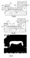
- Figure 5 is an SEM microphotograph illustrating the anisotropy of the titanium nitride etch, using a photoresist mask.
- the structure of Figure 5 illustrates such an etch, in the case where the plasma etch using carbon tetrachloride was extended 200% after clearing of the titanium nitride from the silicide layer (i.e., the etch time was doubled after detection of the clearing of the silicide). After this overetch, the titanium nitride filaments were fully removed from the gate sidewalls (not shown), and as shown in Figure 5, there was insignificant undercut of the titanium nitride under the photoresist mask.
- the selectivity of the chlorine-based etch both to the underlying silicide as well as to oxide and photoresist, as described hereinabove, is especially useful in removing the filaments, as the ability to overetch and thus take advantage of the selective anisotropy phenomenon could not be utilized if the material underlying the titanium interconnect compound (oxide, silicide, or another conductor) or if the photoresist mask (on the order of 600 nm thick over a 100 nm thick titanium nitride film) were also being etched by this etch.
- a thin veneer consisting of some sort of residual material may yet remain on the sides of steps in the structure (e.g., the sides of sidewall oxide 26).
- the composition of such material is not yet well understood, but the material is very thin and quite conductive. Accordingly, a very brief wet etch may still be useful in some cases to remove this interfacial veneer; however, since filaments of the interconnect material itself can be removed by a plasma overetch according to the selective anisotropy described above, the interfacial layer may be removed by an extremely brief etch, with minimal line width reduction of layer 43.
- the selective anisotropy thus can reduce the duration of the wet interfacial layer strip and retain substantially the full line width of layer 43.
Landscapes
- Internal Circuitry In Semiconductor Integrated Circuit Devices (AREA)
- Electrodes Of Semiconductors (AREA)
- Drying Of Semiconductors (AREA)
Applications Claiming Priority (2)
| Application Number | Priority Date | Filing Date | Title |
|---|---|---|---|
| US07/402,944 US4957590A (en) | 1988-02-22 | 1989-09-05 | Method for forming local interconnects using selective anisotropy |
| US402944 | 1989-09-05 |
Publications (2)
| Publication Number | Publication Date |
|---|---|
| EP0416287A2 true EP0416287A2 (fr) | 1991-03-13 |
| EP0416287A3 EP0416287A3 (en) | 1992-08-05 |
Family
ID=23593908
Family Applications (1)
| Application Number | Title | Priority Date | Filing Date |
|---|---|---|---|
| EP19900114835 Withdrawn EP0416287A3 (en) | 1989-09-05 | 1990-08-02 | Improved method for forming local interconnects using selective anisotropy |
Country Status (4)
| Country | Link |
|---|---|
| US (1) | US4957590A (fr) |
| EP (1) | EP0416287A3 (fr) |
| JP (1) | JP3152428B2 (fr) |
| KR (1) | KR0165541B1 (fr) |
Cited By (1)
| Publication number | Priority date | Publication date | Assignee | Title |
|---|---|---|---|---|
| EP0683514A1 (fr) * | 1994-05-19 | 1995-11-22 | International Business Machines Corporation | Masque/isolant surplombant pour interconnections locales et son procédé de fabrication |
Families Citing this family (27)
| Publication number | Priority date | Publication date | Assignee | Title |
|---|---|---|---|---|
| US5122225A (en) * | 1990-11-21 | 1992-06-16 | Texas Instruments Incorporated | Selective etch method |
| JP3185150B2 (ja) * | 1991-03-15 | 2001-07-09 | 日本テキサス・インスツルメンツ株式会社 | 半導体装置の製造方法 |
| JPH05243178A (ja) * | 1991-10-03 | 1993-09-21 | Hewlett Packard Co <Hp> | 半導体集積回路用相互接続体形成方法 |
| US5164331A (en) * | 1991-10-03 | 1992-11-17 | Hewlett-Packard Company | Method of forming and etching titanium-tungsten interconnects |
| US5420071A (en) * | 1993-06-30 | 1995-05-30 | Burke; Edmund | Methods of forming local interconnections in semiconductor devices |
| JP3256048B2 (ja) * | 1993-09-20 | 2002-02-12 | 富士通株式会社 | 半導体装置及びその製造方法 |
| US5468296A (en) * | 1993-12-17 | 1995-11-21 | Lsi Logic Corporation | Apparatus for igniting low pressure inductively coupled plasma |
| JP3238820B2 (ja) * | 1994-02-18 | 2001-12-17 | 富士通株式会社 | 半導体装置 |
| JPH07263544A (ja) * | 1994-03-17 | 1995-10-13 | Fujitsu Ltd | 半導体装置及びその製造方法 |
| US5514908A (en) * | 1994-04-29 | 1996-05-07 | Sgs-Thomson Microelectronics, Inc. | Integrated circuit with a titanium nitride contact barrier having oxygen stuffed grain boundaries |
| US5610099A (en) * | 1994-06-28 | 1997-03-11 | Ramtron International Corporation | Process for fabricating transistors using composite nitride structure |
| US5696428A (en) * | 1995-06-07 | 1997-12-09 | Lsi Logic Corporation | Apparatus and method using optical energy for specifying and quantitatively controlling chemically-reactive components of semiconductor processing plasma etching gas |
| US5935877A (en) * | 1995-09-01 | 1999-08-10 | Applied Materials, Inc. | Etch process for forming contacts over titanium silicide |
| KR0175030B1 (ko) * | 1995-12-07 | 1999-04-01 | 김광호 | 반도체 소자의 고내열 금속 배선 구조 및 그 형성 방법 |
| US6139647A (en) * | 1995-12-21 | 2000-10-31 | International Business Machines Corporation | Selective removal of vertical portions of a film |
| US5767017A (en) * | 1995-12-21 | 1998-06-16 | International Business Machines Corporation | Selective removal of vertical portions of a film |
| KR100198634B1 (ko) * | 1996-09-07 | 1999-06-15 | 구본준 | 반도체 소자의 배선구조 및 제조방법 |
| JP3129232B2 (ja) * | 1997-05-08 | 2001-01-29 | 日本電気株式会社 | 半導体装置の製造方法 |
| US6448655B1 (en) * | 1998-04-28 | 2002-09-10 | International Business Machines Corporation | Stabilization of fluorine-containing low-k dielectrics in a metal/insulator wiring structure by ultraviolet irradiation |
| US6358788B1 (en) * | 1999-08-30 | 2002-03-19 | Micron Technology, Inc. | Method of fabricating a wordline in a memory array of a semiconductor device |
| US6236091B1 (en) * | 1999-09-30 | 2001-05-22 | Advanced Micro Devices, Inc. | Method of forming a local interconnect with improved etch selectivity of silicon dioxide/silicide |
| US6352867B1 (en) * | 2000-01-05 | 2002-03-05 | Advanced Micro Devices, Inc. | Method of controlling feature dimensions based upon etch chemistry concentrations |
| US6953724B2 (en) * | 2003-09-25 | 2005-10-11 | International Business Machines Corporation | Self-limited metal recess for deep trench metal fill |
| US7091085B2 (en) * | 2003-11-14 | 2006-08-15 | Micron Technology, Inc. | Reduced cell-to-cell shorting for memory arrays |
| JP2008010679A (ja) * | 2006-06-29 | 2008-01-17 | Canon Inc | 半導体装置及び半導体装置の製造方法 |
| KR102545968B1 (ko) * | 2014-08-05 | 2023-06-20 | 도쿄엘렉트론가부시키가이샤 | 마이크로전자 기판 상에서의 드라이 하드 마스크 제거의 방법 |
| JP6823533B2 (ja) * | 2017-04-24 | 2021-02-03 | 東京エレクトロン株式会社 | チタンシリサイド領域を形成する方法 |
Family Cites Families (8)
| Publication number | Priority date | Publication date | Assignee | Title |
|---|---|---|---|---|
| US4574177A (en) * | 1982-02-01 | 1986-03-04 | Texas Instruments Incorporated | Plasma etch method for TiO2 |
| US4450042A (en) * | 1982-07-06 | 1984-05-22 | Texas Instruments Incorporated | Plasma etch chemistry for anisotropic etching of silicon |
| US4676866A (en) * | 1985-05-01 | 1987-06-30 | Texas Instruments Incorporated | Process to increase tin thickness |
| US4657628A (en) * | 1985-05-01 | 1987-04-14 | Texas Instruments Incorporated | Process for patterning local interconnects |
| US4675073A (en) * | 1986-03-07 | 1987-06-23 | Texas Instruments Incorporated | Tin etch process |
| US4690730A (en) * | 1986-03-07 | 1987-09-01 | Texas Instruments Incorporated | Oxide-capped titanium silicide formation |
| US4784973A (en) * | 1987-08-24 | 1988-11-15 | Inmos Corporation | Semiconductor contact silicide/nitride process with control for silicide thickness |
| US4793896C1 (en) * | 1988-02-22 | 2001-10-23 | Texas Instruments Inc | Method for forming local interconnects using chlorine bearing agents |
-
1989
- 1989-09-05 US US07/402,944 patent/US4957590A/en not_active Expired - Lifetime
-
1990
- 1990-08-02 EP EP19900114835 patent/EP0416287A3/en not_active Withdrawn
- 1990-09-04 JP JP23432990A patent/JP3152428B2/ja not_active Expired - Fee Related
- 1990-09-04 KR KR1019900013925A patent/KR0165541B1/ko not_active Expired - Fee Related
Cited By (1)
| Publication number | Priority date | Publication date | Assignee | Title |
|---|---|---|---|---|
| EP0683514A1 (fr) * | 1994-05-19 | 1995-11-22 | International Business Machines Corporation | Masque/isolant surplombant pour interconnections locales et son procédé de fabrication |
Also Published As
| Publication number | Publication date |
|---|---|
| JP3152428B2 (ja) | 2001-04-03 |
| EP0416287A3 (en) | 1992-08-05 |
| JPH03261139A (ja) | 1991-11-21 |
| KR910007087A (ko) | 1991-04-30 |
| US4957590A (en) | 1990-09-18 |
| KR0165541B1 (ko) | 1999-02-01 |
Similar Documents
| Publication | Publication Date | Title |
|---|---|---|
| US4957590A (en) | Method for forming local interconnects using selective anisotropy | |
| EP0332833B1 (fr) | Méthode pour la formation d'interconnexions locales avec des agents chlorés | |
| US4470189A (en) | Process for making polycide structures | |
| US5122225A (en) | Selective etch method | |
| US5318924A (en) | Nitridation of titanium-tungsten interconnects | |
| US4690730A (en) | Oxide-capped titanium silicide formation | |
| US5610099A (en) | Process for fabricating transistors using composite nitride structure | |
| KR100530401B1 (ko) | 저저항 게이트 전극을 구비하는 반도체 장치 | |
| EP0442718B1 (fr) | Procédé de fabrication d'un dispositif semi-conducteur | |
| US6846739B1 (en) | MOCVD process using ozone as a reactant to deposit a metal oxide barrier layer | |
| US5086017A (en) | Self aligned silicide process for gate/runner without extra masking | |
| US5164331A (en) | Method of forming and etching titanium-tungsten interconnects | |
| US6858934B2 (en) | Semiconductor device structures including metal silicide interconnect structures that extend at least partially over transistor gate structures and methods for making the same | |
| US6204170B1 (en) | Method for manufacturing semiconductor device having metal silicide film and metal film in which metal film can be selectively removed | |
| US4980020A (en) | Local interconnect etch technique | |
| US6277758B1 (en) | Method of etching doped silicon dioxide with selectivity to undoped silicon dioxide with a high density plasma etcher | |
| US5280190A (en) | Self aligned emitter/runner integrated circuit | |
| US6960531B2 (en) | Method of manufacturing electronic device | |
| Levy et al. | Selective LPCVD tungsten for contact barrier applications | |
| US6847085B2 (en) | High aspect ratio contact surfaces having reduced contaminants | |
| US6774029B2 (en) | Method for forming a conductive film and a conductive pattern of a semiconductor device | |
| Tsutsumi et al. | A selective LPCVD tungsten process using silane reduction for VLSI applications | |
| JPH08339987A (ja) | 配線形成方法 |
Legal Events
| Date | Code | Title | Description |
|---|---|---|---|
| PUAI | Public reference made under article 153(3) epc to a published international application that has entered the european phase |
Free format text: ORIGINAL CODE: 0009012 |
|
| AK | Designated contracting states |
Kind code of ref document: A2 Designated state(s): DE FR GB IT NL |
|
| PUAL | Search report despatched |
Free format text: ORIGINAL CODE: 0009013 |
|
| AK | Designated contracting states |
Kind code of ref document: A3 Designated state(s): DE FR GB IT NL |
|
| 17P | Request for examination filed |
Effective date: 19930107 |
|
| 17Q | First examination report despatched |
Effective date: 19940816 |
|
| STAA | Information on the status of an ep patent application or granted ep patent |
Free format text: STATUS: THE APPLICATION IS DEEMED TO BE WITHDRAWN |
|
| 18D | Application deemed to be withdrawn |
Effective date: 19950228 |