EP0416345A2 - Décodeur d'instructions pour un processeur pipeline - Google Patents
Décodeur d'instructions pour un processeur pipeline Download PDFInfo
- Publication number
- EP0416345A2 EP0416345A2 EP90115715A EP90115715A EP0416345A2 EP 0416345 A2 EP0416345 A2 EP 0416345A2 EP 90115715 A EP90115715 A EP 90115715A EP 90115715 A EP90115715 A EP 90115715A EP 0416345 A2 EP0416345 A2 EP 0416345A2
- Authority
- EP
- European Patent Office
- Prior art keywords
- purpose register
- register part
- special purpose
- processing apparatus
- register
- Prior art date
- Legal status (The legal status is an assumption and is not a legal conclusion. Google has not performed a legal analysis and makes no representation as to the accuracy of the status listed.)
- Granted
Links
Images








Classifications
-
- G—PHYSICS
- G06—COMPUTING OR CALCULATING; COUNTING
- G06F—ELECTRIC DIGITAL DATA PROCESSING
- G06F9/00—Arrangements for program control, e.g. control units
- G06F9/06—Arrangements for program control, e.g. control units using stored programs, i.e. using an internal store of processing equipment to receive or retain programs
- G06F9/30—Arrangements for executing machine instructions, e.g. instruction decode
- G06F9/38—Concurrent instruction execution, e.g. pipeline or look ahead
- G06F9/3824—Operand accessing
-
- G—PHYSICS
- G06—COMPUTING OR CALCULATING; COUNTING
- G06F—ELECTRIC DIGITAL DATA PROCESSING
- G06F9/00—Arrangements for program control, e.g. control units
- G06F9/06—Arrangements for program control, e.g. control units using stored programs, i.e. using an internal store of processing equipment to receive or retain programs
- G06F9/30—Arrangements for executing machine instructions, e.g. instruction decode
- G06F9/30098—Register arrangements
- G06F9/30101—Special purpose registers
-
- G—PHYSICS
- G06—COMPUTING OR CALCULATING; COUNTING
- G06F—ELECTRIC DIGITAL DATA PROCESSING
- G06F9/00—Arrangements for program control, e.g. control units
- G06F9/06—Arrangements for program control, e.g. control units using stored programs, i.e. using an internal store of processing equipment to receive or retain programs
- G06F9/30—Arrangements for executing machine instructions, e.g. instruction decode
- G06F9/30145—Instruction analysis, e.g. decoding, instruction word fields
- G06F9/3016—Decoding the operand specifier, e.g. specifier format
Definitions
- the present invention generally relates to information processing apparatuses, and more particularly to an information processing apparatus for processing digital data at a high data processing speed and suited for application on a general purpose microprocessor.
- the operation frequency is high and a processing such as the pipeline processing is carried out to satisfy the demands for high-speed data processing.
- the pipeline processing of the microprocessor is made up of five stages which are an instruction decode stage, an effective address calculation stage, an operand read stage, an operand process execution stage and an operand write stage.
- the read out from the register and the decoding of the instruction must be carried out in the instruction decode stage in order to enter the effective address calculation stage.
- the instruction decode stage in order to realize the high-speed data processing, the instruction decode stage must be carried out at a high speed, that is, the read out from the register and the decoding of the instruction must be carried out at a high speed.
- FIG.1 shows an example of a conventional information processing apparatus.
- An information processing apparatus 50 shown in FIG.1 includes an instruction register 51 for storing an instruction, a bus 58 for transferring the instruction, an instruction decoder 52 for decoding the transferred instruction, a register specifier part 53 for specifying a register depending on a decoded result from the instruction decoder 52, a general purpose register part 54 including a stack pointer and a plurality of general purpose registers, a special purpose register part 55 including a plurality of special purpose registers, an address calculation part 56 for calculating an effective address from the decoded result and a read out register content, and a memory 57 to which an access is made based on a calculation result.
- the information processing apparatus 50 transfers an instruction code within the instruction to the instruction decoder 52 via the bus 58.
- the instruction decoder 52 decodes the instruction code and supplies a decoded result to the register specifier part 53.
- the register specifier part 53 specifies a read operation from the general purpose register part 54 or the special purpose register part 55.
- the address calculation part 56 calculates the effective address and makes access to the memory 57 at this effective address. Thereafter, the information processing apparatus 50 carries out various processes based on the contents of the memory 57 and the like.
- the stack pointer When the stack pointer is specified by the general purpose register part 54, the stack pointer may be read out as the stack pointer itself and the stack pointer may be read out as the general purpose register depending on the decoded result. For this reason, an access to the register can only be made after the decoding of the instruction. Therefore, there is a problem in that the speed of the decoding stage cannot be reduced considerably, and it is thus difficult to set the operation frequency high.
- Another and more specific object of the present invention is to provide an information processing apparatus comprising a decoder for decoding an instruction, a general purpose register part including a stack pointer and a plurality of general purpose registers, a special purpose register part including a plurality of special purpose registers, and processing means coupled to the decoder, the general purpose register part and the special purpose register part for carrying out a predetermined process based on a decoded result from the decoder by selectively using a read out result of one of the general purpose register part and the special purpose register part.
- a decoding operation of the decoder, a read out operation of the general purpose register part and a read out operation of the special purpose register part are carried out in parallel. According to the information processing apparatus of the present invention, it is possible to increase the processing speed of the instruction decode stage of the pipeline processing and to increase the processing speed of the effective address calculation stage which follows. Therefore, the processing speed of the information processing apparatus is greatly increased.
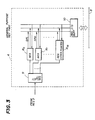
- An information processing apparatus 1 shown in FIG.2 includes an instruction register 2 for temporarily storing an instruction, an instruction decoder 3 for decoding an instruction code within the instruction and for outputting a register specifying signal 11 which selects a general purpose register or a special purpose register which will be described later, a general purpose register part 4 including a stack pointer and a plurality of general purpose registers, a special purpose register part 5 including a plurality of special purpose registers, an address calculation part 6 for calculating an address from a result of the decoded instruction and a register content, a memory to which an access is made based on the address calculated in the address calculation part 6, and a bus part 8 for transmitting and receiving data.
- an instruction register 2 for temporarily storing an instruction
- an instruction decoder 3 for decoding an instruction code within the instruction and for outputting a register specifying signal 11 which selects a general purpose register or a special purpose register which will be described later
- a general purpose register part 4 including a stack pointer and a plurality of general purpose registers
- the information processing apparatus 1 is made of a monolithic microprocessor which is formed on a single semiconductor body.
- the general purpose register part 4 includes sixteen registers R0 through R15 for storing various data, a general purpose register selection circuit 9 for selecting a predetermined one of the registers R0 through R15, and a register input/output buffer 10 for temporarily storing the data when inputting/outputting data.
- the register R15 of the general purpose register part 4 is used as the stack pointer.
- the special purpose register part 5 has a structure similar to that of the general purpose register part 4, and illustration and description thereof will be omitted.
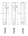
- FIGS.4A through 4C show instruction formats which may be employed in this embodiment.
- FIGS.4A and 4B show instruction formats having an effective address field ADRF within an instruction W for specifying an effective address.
- a register field RF for specifying a register is provided within the effective address field ADRF.
- FIG.4C shows an instruction format having no effective address field ADRF.
- the instruction length is L.
- the instruction decoder 3 decodes an instruction code CODE within the instruction W.
- the information processing apparatus 1 specifies a general purpose register number based on the contents of the register field RF within the instruction W in the cases shown in FIGS.4A and 4B or based on the contents at a location where a register field should exist within the instruction W when no register field RF exists as shown in FIG.4C.
- the general purpose register number is used to make access to a general purpose register which is specified by the general purpose register number.
- an access is simultaneously made to a special purpose register depending on the running state.
- the instruction decoder 3 outputs the register specifying signal 11 based on the decoded result of the instruction code CODE. Based on this register specifying signal 11, a result of the access to the general purpose register part 4 or a result of the access to the special purpose register part 5 is transferred to the address calculation part 6 via the bus part 8.
- the address calculation part 6 calculates an actual address in the memory 7 based on the decoded result of the instruction code CODE and the result of the access to the general purpose register part 4 or the result of the access to the special purpose register part 5.
- the information processing apparatus 1 carries out a processing based on the actual address calculated in the address calculation part 6.
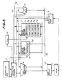
- FIG.5 a description will be given of a second embodiment of the information processing apparatus according to the present invention, by referring to FIG.5.
- the present invention is applied to an information processing apparatus having TRON (The Realtime Operating System Nucleus) specifications.
- TRON The Realtime Operating System Nucleus
- FIG.5 those parts which are essentially the same as those corresponding parts in FIG.2 are designated by the same reference numerals, and a description thereof will be omitted.
- This second embodiment differs from the first embodiment described above in that this second embodiment includes five stack pointers S1 through S5 in the special purpose register part 5 and a data input/output part 12, an arithmetic logic unit (ALU) 13, a processor status word register 15 and an address output part 19 are further provided.
- the data input/output part 12 carries out an interface operation with respect to the input/output data, and the ALU 13 carries out the actual operation process.
- the processor status word stored in the processor status word register 15 is supplied to the special purpose register part 5 responsive to the instruction decoder 3.
- the address output part 19 supplies the address from the address calculation part 6 to the memory 7.
- a ring protection method is employed in order to prevent destruction of a system region due to a bug in the program.
- the ring protection method takes measures so that a region (including program region, data region and work region) to which an access can be made differs depending on the ring level.
- the ring level "0" is the highest ring level, and the region to which an access can be made becomes larger as the ring level becomes higher. For example, an access can be made to all of the region when the ring level is "0". For this reason, the stack pointers S1 through S4 for making access are respectively provided in correspondence with the four ring levels.
- the stack pointer When making a transition between two ring levels, the stack pointer is switched so that the program having a low ring level will not rewrite the region of the program having a high ring level. In order to make access to the stack pointer, a judgement must first be made to determine the ring level which is presently running. The remaining stack pointer S5 is used as a stack pointer for interrupt processing.
- the register content which is read out is transferred to the address calculation part 6 together with the result of the decoded instruction, and the effective address of the memory 7 is calculated in the address calculation part 6. Thereafter, the data within the memory 7 at the calculated effective address is transferred to the ALU 13 via the data input/output part 12 and processed in the ALU 13.
- the information processing apparatus is made of a monolithic microprocessor which is formed on a single semiconductor body.
- FIG.6 shows an embodiment of the general purpose register part 4 shown in FIG.5.
- the general purpose register part 4 shown in FIG.6 includes a register selection circuit 61 for address calculation, a register address decoding circuit 62 for address calculation, a register data part 63, a bus output circuit 64 for address calculation, a bus output circuit 65 for operation, a register write buffer 66, a register decoding circuit 67 for writing, and a register decoding circuit 68 for operation which are coupled as shown.
- FIG.7 shows an essential part of an embodiment of the register selection circuit 61 shown in FIG.6.
- the register selection circuit 61 includes an inverter 611 which receives a switching signal IRDEC, a gate group 612 and a latch circuit group 613 which are connected as shown.
- the switching signal IRDEC switches the mode between an instruction decode mode and a microinstruction execution mode.
- the gate group 612 receives microinstructions MIAF0 through MIAF3, processor status word signals IR12 through IR15, the switching signal IRDEC and an inverted switching signal IRDEC .
- the latch circuit group 613 receives outputs of the gate group 612 and outputs register selection signals AFREG0 through AFREG3 in response to a clock signal CLK.
- FIG.8 shows an essential part of an embodiment of the register address decoding circuit 62 shown in FIG.6.
- the register address decoding circuit 62 includes an inverter group 621 and decoding circuits 6220 through 62215 having identical circuit structure. Only the circuit structure of the decoding circuit 6220 is shown for the sake of convenience.
- the decoding circuits 6220 through 62215 respectively output selection signals AFREGSEL0 through AFREGSELF in response to the register selection signals AFREG0 through AFREG3 from the register selection circuit 61 and clock signals REGPRE and REGDIS.
- FIG.9 shows an essential part of an embodiment of the register data part 63 shown in FIG.6.
- the register data part 63 includes transistors and inverters which are connected as shown for storing data.
- Signals RDBIT0 and RDBIT0X are obtained from a bus RD via the register write buffer 66.
- a signal AFBIT0 is supplied to the bus output circuit 64, and signals SSBIT0 and SDBIT0 are supplied to the bus output circuit 65.
- Signals RDREGSEL0 and RDREGSELF are obtained from the register decoding circuit 67, and signals SSREGSEL0 and SSREGSELF and signals SDREGSEL0 and SDREGSELF are obtained from the register decoding circuit 68.
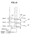
- FIG.10 shows an essential part of an embodiment of the bus output circuits 64 and 65.
- the circuit part shown in FIG.10 includes a latch circuit group 641, a AND gate group 642, a transistor group 643, and a gate circuit part 644.
- the gate circuit part 644 receives the switching signal IRDECD2 for switching the mode between the instruction decode mode and the microinstruction execution mode, a signal MIGREG for controlling the bus output, and an enable signal DECGREG for enabling the instruction decode and read out from the register data part 63.
- Output signals SD0, SS0 and AF0 are respectively output on the buses SD, SS and AF.
- FlG.11 shows an embodiment of the special purpose register part 5 shown in FIG.5.
- the special purpose register part 5 shown in FIG.11 includes a read out selection circuit 71, a register address decoding circuit 72, a special purpose register data part 73, a bus output circuit 74, a register write buffer 75, a write selection circuit 76, and a write register decoding circuit 77 which are coupled as shown.
- FIG.12 shows an essential part of an embodiment of the read out selection circuit 71 shown in FIG.11.
- the read out selection circuit 71 includes an inverter 711 which receives the switching signal IRDEC, a gate group 712 and a latch circuit group 713 which are connected as shown.
- the gate group 712 receives microinstructions MIPREG0 through MIPREG3, ring level signals PSWSM, PSWRNG0 and PSWRNG1 received from the processor status word register 15 shown in FIG.5, the switching signal IRDEC and an inverted switching signal IRDEC .
- the latch circuit group 613 receives outputs of the gate group 612 and outputs register selection signals PREGRD0 through PREGRD3 in response to the clock signal CLK.
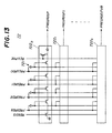
- FIG.13 shows an essential part of an embodiment of the register address decoding circuit 72 shown in FIG.11.
- the register address decoding circuit 72 includes an inverter group 721 and decoding circuits 7220 through 722 n having identical circuit structure. Only the circuit structure of the decoding circuit 7220 is shown for the sake of convenience.
- the decoding circuits 7221, 7222 and 722 n respectively output selection signals PREGRDSP, PREGRDSPI and PREGRDEITVB in response to the register selection signals PREGRD0 through PREGRD3 from the register selection circuit 71 and the clock signals REGPRE and REGDIS.
- the circuit structure of the register address decoding circuit 72 is basically the same as that of the register address decoding circuit 62 shown in FIG.6.
- FIG.14 shows an essential part of an embodiment of the special purpose register data part 73 shown in FIG.11.
- the selection signals PREGRDSPI and PREGRDEITVB are obtained from the register address decoding circuit 72, and signals PREGWRSPI and PREGWREITVB are obtained from the write register decoding circuit 77.
- Signals PWBIT0 and PWBIT0X are obtained from the register write buffer 75, and a signal PRBIT0 is supplied to the bus output circuit 74.
- the circuit structure of the special purpose register data part 73 is similar to that of the general purpose register data part 63 shown in FIG.9.
- FIG.15 shows an essential part of an embodiment of the bus output circuit 74.
- the circuit structure of the bus output circuit 74 is similar to that of the circuit part shown in FIG.10.
- the bus output circuit 74 includes a latch circuit group 741, a AND gate group 742, a transistor group 743, and a gate circuit part 744.
- the gate circuit part 644 receives the switching signal IRDECD2 for switching the mode between the instruction decode mode and the microinstruction execution mode, a signal MIPREG for controlling the bus output, and an enable signal DECPREG for enabling the instruction decode and read out from the register data part 73.
- Output signals AF0 and AF1 are output on the bus AF.
Landscapes
- Engineering & Computer Science (AREA)
- Software Systems (AREA)
- Theoretical Computer Science (AREA)
- Physics & Mathematics (AREA)
- General Engineering & Computer Science (AREA)
- General Physics & Mathematics (AREA)
- Executing Machine-Instructions (AREA)
Applications Claiming Priority (2)
| Application Number | Priority Date | Filing Date | Title |
|---|---|---|---|
| JP1213944A JP2553200B2 (ja) | 1989-08-19 | 1989-08-19 | 情報処理装置 |
| JP213944/89 | 1989-08-19 |
Publications (3)
| Publication Number | Publication Date |
|---|---|
| EP0416345A2 true EP0416345A2 (fr) | 1991-03-13 |
| EP0416345A3 EP0416345A3 (en) | 1993-03-24 |
| EP0416345B1 EP0416345B1 (fr) | 1998-07-22 |
Family
ID=16647635
Family Applications (1)
| Application Number | Title | Priority Date | Filing Date |
|---|---|---|---|
| EP90115715A Expired - Lifetime EP0416345B1 (fr) | 1989-08-19 | 1990-08-16 | Décodeur d'instructions pour un processeur pipeline |
Country Status (4)
| Country | Link |
|---|---|
| EP (1) | EP0416345B1 (fr) |
| JP (1) | JP2553200B2 (fr) |
| KR (1) | KR940009377B1 (fr) |
| DE (1) | DE69032494T2 (fr) |
Cited By (4)
| Publication number | Priority date | Publication date | Assignee | Title |
|---|---|---|---|---|
| EP0605927A1 (fr) * | 1992-12-29 | 1994-07-13 | Koninklijke Philips Electronics N.V. | Architecture améliorée pour processeur à mot d'instruction très long |
| GB2321121A (en) * | 1996-10-24 | 1998-07-15 | Nec Corp | Microprocessor has DSP functions |
| GB2421091A (en) * | 2004-12-07 | 2006-06-14 | Hewlett Packard Development Co | Processor for a memory tag |
| US11204768B2 (en) | 2019-11-06 | 2021-12-21 | Onnivation Llc | Instruction length based parallel instruction demarcator |
Families Citing this family (1)
| Publication number | Priority date | Publication date | Assignee | Title |
|---|---|---|---|---|
| JPH1091432A (ja) * | 1996-09-13 | 1998-04-10 | Sanyo Electric Co Ltd | プログラム実行方法およびプログラム実行装置 |
Family Cites Families (5)
| Publication number | Priority date | Publication date | Assignee | Title |
|---|---|---|---|---|
| JPS5824947A (ja) * | 1981-08-07 | 1983-02-15 | Hitachi Ltd | 情報処理装置 |
| JPS58142464A (ja) * | 1982-02-19 | 1983-08-24 | Hitachi Ltd | マイクロプロセツサ |
| JPS607540A (ja) * | 1983-06-24 | 1985-01-16 | Mitsubishi Electric Corp | 割込制御回路 |
| JPH0744877B2 (ja) * | 1986-04-18 | 1995-05-15 | 富士通株式会社 | パルスモ−タ駆動回路 |
| EP0314079B1 (fr) * | 1987-10-27 | 1992-05-06 | Siemens Nixdorf Informationssysteme Aktiengesellschaft | Disposition de circuit pour les unités d'éxécution d'une unité centrale comprenant une pluralité de registres à usage général |
-
1989
- 1989-08-19 JP JP1213944A patent/JP2553200B2/ja not_active Expired - Fee Related
-
1990
- 1990-08-16 EP EP90115715A patent/EP0416345B1/fr not_active Expired - Lifetime
- 1990-08-16 DE DE69032494T patent/DE69032494T2/de not_active Expired - Fee Related
- 1990-08-17 KR KR1019900012698A patent/KR940009377B1/ko not_active Expired - Fee Related
Cited By (6)
| Publication number | Priority date | Publication date | Assignee | Title |
|---|---|---|---|---|
| EP0605927A1 (fr) * | 1992-12-29 | 1994-07-13 | Koninklijke Philips Electronics N.V. | Architecture améliorée pour processeur à mot d'instruction très long |
| GB2321121A (en) * | 1996-10-24 | 1998-07-15 | Nec Corp | Microprocessor has DSP functions |
| GB2321121B (en) * | 1996-10-24 | 2001-06-20 | Nec Corp | Microprocessor |
| GB2421091A (en) * | 2004-12-07 | 2006-06-14 | Hewlett Packard Development Co | Processor for a memory tag |
| GB2421091B (en) * | 2004-12-07 | 2008-09-03 | Hewlett Packard Development Co | Central processor for a memory tag |
| US11204768B2 (en) | 2019-11-06 | 2021-12-21 | Onnivation Llc | Instruction length based parallel instruction demarcator |
Also Published As
| Publication number | Publication date |
|---|---|
| EP0416345A3 (en) | 1993-03-24 |
| KR940009377B1 (ko) | 1994-10-07 |
| DE69032494D1 (de) | 1998-08-27 |
| JPH0377137A (ja) | 1991-04-02 |
| EP0416345B1 (fr) | 1998-07-22 |
| JP2553200B2 (ja) | 1996-11-13 |
| KR910005152A (ko) | 1991-03-30 |
| DE69032494T2 (de) | 1999-02-18 |
Similar Documents
| Publication | Publication Date | Title |
|---|---|---|
| US5511173A (en) | Programmable logic array and data processing unit using the same | |
| EP0169565B1 (fr) | Microprocesseur compatible avec chaque logiciel représenté par différents types de formats d'instructions | |
| EP0740249B1 (fr) | Dispositif de traitement de données avec coprocesseur | |
| US5511207A (en) | Program control circuit determining the designated number of times a sequence of instructions is repetitively executed to prevent further execution of a jump instruction | |
| EP0220684B1 (fr) | Système de traitement de données | |
| US4774688A (en) | Data processing system for determining min/max in a single operation cycle as a result of a single instruction | |
| EP0533337A1 (fr) | Dispositif et procédé pour résoudre les dépendances entre plusieurs instructions dans une mémoire | |
| EP0199173B1 (fr) | Système de traitement de données | |
| US4523277A (en) | Priority interrupt system for microcomputer | |
| EP0323140B1 (fr) | Dispositif de traitement de données | |
| US6581120B1 (en) | Interrupt controller | |
| US5274792A (en) | Information processing apparatus with parallel instruction decoding | |
| EP0223150B1 (fr) | Dispositif de traitement d'information | |
| EP0338564B1 (fr) | Méthode de branchement d'un microprogramme et microséquenceur l'utilisant | |
| KR920003180B1 (ko) | 바이패스(bypass)회로를 갖는 데이타 처리장치 | |
| EP0416345B1 (fr) | Décodeur d'instructions pour un processeur pipeline | |
| US5539900A (en) | Information processing system | |
| US5742842A (en) | Data processing apparatus for executing a vector operation under control of a master processor | |
| US5604876A (en) | Apparatus for handling differing data length instructions using either directly specified or indirectly specified data lengths | |
| EP0325226B1 (fr) | Appareil et méthode de traitement et d'information | |
| EP0334131B1 (fr) | Processeur de données exécutant une opération sur des données de longueur inférieure à un mot | |
| US5931941A (en) | Interface for a modularized computational unit to a CPU | |
| EP0343668B1 (fr) | Système de commande de normalisation pour des opérations arithmétiques à virgule flottante | |
| EP0136699A2 (fr) | Unité de commande programmable | |
| EP0352745A2 (fr) | Microprocesseur |
Legal Events
| Date | Code | Title | Description |
|---|---|---|---|
| PUAI | Public reference made under article 153(3) epc to a published international application that has entered the european phase |
Free format text: ORIGINAL CODE: 0009012 |
|
| AK | Designated contracting states |
Kind code of ref document: A2 Designated state(s): DE FR GB |
|
| PUAL | Search report despatched |
Free format text: ORIGINAL CODE: 0009013 |
|
| AK | Designated contracting states |
Kind code of ref document: A3 Designated state(s): DE FR GB |
|
| 17P | Request for examination filed |
Effective date: 19930921 |
|
| 17Q | First examination report despatched |
Effective date: 19951221 |
|
| GRAG | Despatch of communication of intention to grant |
Free format text: ORIGINAL CODE: EPIDOS AGRA |
|
| GRAG | Despatch of communication of intention to grant |
Free format text: ORIGINAL CODE: EPIDOS AGRA |
|
| GRAH | Despatch of communication of intention to grant a patent |
Free format text: ORIGINAL CODE: EPIDOS IGRA |
|
| RBV | Designated contracting states (corrected) |
Designated state(s): DE |
|
| GRAH | Despatch of communication of intention to grant a patent |
Free format text: ORIGINAL CODE: EPIDOS IGRA |
|
| GRAA | (expected) grant |
Free format text: ORIGINAL CODE: 0009210 |
|
| AK | Designated contracting states |
Kind code of ref document: B1 Designated state(s): DE |
|
| REF | Corresponds to: |
Ref document number: 69032494 Country of ref document: DE Date of ref document: 19980827 |
|
| PLBE | No opposition filed within time limit |
Free format text: ORIGINAL CODE: 0009261 |
|
| STAA | Information on the status of an ep patent application or granted ep patent |
Free format text: STATUS: NO OPPOSITION FILED WITHIN TIME LIMIT |
|
| 26N | No opposition filed | ||
| PGFP | Annual fee paid to national office [announced via postgrant information from national office to epo] |
Ref country code: DE Payment date: 20060810 Year of fee payment: 17 |
|
| PG25 | Lapsed in a contracting state [announced via postgrant information from national office to epo] |
Ref country code: DE Free format text: LAPSE BECAUSE OF NON-PAYMENT OF DUE FEES Effective date: 20080301 |