EP0416488A2 - Méthode et dispositif fournissant un signal de blocage de coupure pour un semi-conducteur de puissance à extinction - Google Patents
Méthode et dispositif fournissant un signal de blocage de coupure pour un semi-conducteur de puissance à extinction Download PDFInfo
- Publication number
- EP0416488A2 EP0416488A2 EP90116824A EP90116824A EP0416488A2 EP 0416488 A2 EP0416488 A2 EP 0416488A2 EP 90116824 A EP90116824 A EP 90116824A EP 90116824 A EP90116824 A EP 90116824A EP 0416488 A2 EP0416488 A2 EP 0416488A2
- Authority
- EP
- European Patent Office
- Prior art keywords
- current
- converter
- load
- load current
- phase
- Prior art date
- Legal status (The legal status is an assumption and is not a legal conclusion. Google has not performed a legal analysis and makes no representation as to the accuracy of the status listed.)
- Withdrawn
Links
Images
Classifications
-
- H—ELECTRICITY
- H02—GENERATION; CONVERSION OR DISTRIBUTION OF ELECTRIC POWER
- H02M—APPARATUS FOR CONVERSION BETWEEN AC AND AC, BETWEEN AC AND DC, OR BETWEEN DC AND DC, AND FOR USE WITH MAINS OR SIMILAR POWER SUPPLY SYSTEMS; CONVERSION OF DC OR AC INPUT POWER INTO SURGE OUTPUT POWER; CONTROL OR REGULATION THEREOF
- H02M1/00—Details of apparatus for conversion
- H02M1/06—Circuits specially adapted for rendering non-conductive gas discharge tubes or equivalent semiconductor devices, e.g. thyratrons, thyristors
-
- H—ELECTRICITY
- H02—GENERATION; CONVERSION OR DISTRIBUTION OF ELECTRIC POWER
- H02M—APPARATUS FOR CONVERSION BETWEEN AC AND AC, BETWEEN AC AND DC, OR BETWEEN DC AND DC, AND FOR USE WITH MAINS OR SIMILAR POWER SUPPLY SYSTEMS; CONVERSION OF DC OR AC INPUT POWER INTO SURGE OUTPUT POWER; CONTROL OR REGULATION THEREOF
- H02M7/00—Conversion of AC power input into DC power output; Conversion of DC power input into AC power output
- H02M7/42—Conversion of DC power input into AC power output without possibility of reversal
- H02M7/44—Conversion of DC power input into AC power output without possibility of reversal by static converters
- H02M7/48—Conversion of DC power input into AC power output without possibility of reversal by static converters using discharge tubes with control electrode or semiconductor devices with control electrode
- H02M7/505—Conversion of DC power input into AC power output without possibility of reversal by static converters using discharge tubes with control electrode or semiconductor devices with control electrode using devices of a thyratron or thyristor type requiring extinguishing means
- H02M7/515—Conversion of DC power input into AC power output without possibility of reversal by static converters using discharge tubes with control electrode or semiconductor devices with control electrode using devices of a thyratron or thyristor type requiring extinguishing means using semiconductor devices only
- H02M7/5152—Conversion of DC power input into AC power output without possibility of reversal by static converters using discharge tubes with control electrode or semiconductor devices with control electrode using devices of a thyratron or thyristor type requiring extinguishing means using semiconductor devices only with separate extinguishing means
- H02M7/5155—Conversion of DC power input into AC power output without possibility of reversal by static converters using discharge tubes with control electrode or semiconductor devices with control electrode using devices of a thyratron or thyristor type requiring extinguishing means using semiconductor devices only with separate extinguishing means wherein each commutation element has its own extinguishing means
Definitions
- the invention relates to a method for forming an erase inhibit signal for power semiconductors which can be switched off in power converters to suppress inadmissible attempts to erase and to a device therefor.
- One application is e.g. possible with GTO pulse inverters for traction drives.
- Such a method is known from DE-OS 37 27 996.
- the method described there for suppressing inadmissible extinguishing attempts in the case of power semiconductors which can be switched off in power converters is characterized in that a measured variable composed of the current anode current or load current of the semiconductor and the product of the time derivative of the current anode current and the maximum switch-off delay time is formed and can be set with an adjustable value , maximum switchable anode current is compared, with occurring Deletion commands are suppressed when the measured variable formed reaches or exceeds the maximum switchable anode current.
- ITQ periodically switchable anode current of a GTO thyristor
- a GTO thyristor only interrupts the current for a certain time - the so-called storage time - after the switch-off command.
- the anode current of the GTO thyristor can increase further during the storage time.
- the method of the predictive extinguishing block according to DE-OS 37 27 996 therefore estimates the current to be expected from the current GTO current and its current increase (di / dt) during the storage time at the moment of switching off the GTO thyristor and compares it with ITQ.
- the load current of the converter can be used in the known method, since this is measured anyway for control purposes and usually differs only slightly from the GTO current.
- the di / dt values of the GTO currents are measured individually by detection coils (current rise detection devices) for each GTO thyristor.
- the di / dt detection coils can only be installed in such a way that they are also exposed to the currents of the relief networks for the GTO thyristors.
- the relief networks are LC structures (L: inductance, C: condensate gate), which vibrate more or less depending on the circuit used in the power unit. Since the di / dt detection coils measure the wiring currents in the known method, in practice, errors in the formation of the extinguishing blocking signal can occur due to the high di / dt values of the wiring vibrations.
- the extinguishing block is triggered incorrectly and unnecessarily. These false triggers have to be filtered out again at the signal processing level. If the di / dt value of the wiring current is opposite to that of the GTO current, the extinguishing barrier assumes that the di / dt value is too small and therefore may not trigger, although this would be necessary. The consequence is a risk of destruction for the affected GTO thyristor.
- the invention has for its object to provide a method for forming an erase inhibit signal for power semiconductors that can be switched off, which ensures maximum utilization in a simple manner without risk of destruction for the power semiconductors and largely avoids malfunctions due to wiring currents in relief networks for the power semiconductors. Furthermore, a device for this purpose is to be developed.
- This object is achieved with respect to the method for forming an extinguishing block signal for power semiconductors which can be switched off in power converters to suppress inadmissible attempts to extinguish them, in that an extinguishing block signal is emitted when the sum of the current load current of a phase of the converter and the product of the time derivative of the load current and the maximum storage time of a power semiconductor is greater than the maximum, periodically switchable anode current of a power semiconductor.
- the advantages that can be achieved with the invention are, in particular, that the analog measured values of the current rise detection devices in the power semiconductor branches (GTO branches) do not directly contribute to the generation of the predictive extinguishing barrier, and thus the disturbing influences of the circuit transients (di / dt values of the circuit currents in the relief networks for the power semiconductors or GTO thyristors) are eliminated.
- the digitally generated short-circuit message is hardly disturbed by wiring currents because of the relatively high comparator threshold of the comparator to be used.
- the effort for the measurement value acquisition is reduced by the invention, because a single current rise detection device is sufficient for each string of a three-phase GTO inverter in bridge circuit having two GTO thyristors.
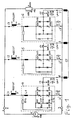
- FIG. 1 shows the diagram of a GTO inverter with various measuring devices for the formation of extinguishing blocking signals.
- a DC voltage source 1 can be seen, between the positive pole 2 or negative pole 3 of which three strands 4, 5, 6 of a three-phase GTO inverter to be operated on a DC voltage intermediate circuit are connected.
- the three-phase bridge GTO inverter has six branches, each with a GTO thyristor V11, V21, V31, V12, V22, V32 (generally: power semiconductors that can be switched off) as main valves.
- Each GTO thyristor has a diode V13, V23, V33, V14, V24, V34 anti-parallel.
- the control device for igniting and extinguishing the GTO thyristors is not shown in FIG. 1 for reasons of clarity.
- Each string 4, 5, 6 of the GTO inverter has a relief network consisting of a generally known arrangement of diodes V15, V16 ...., capacitors C11, C12, C13 ..., resistors R11, R12, .... and chokes L1 ..., only the components of the relief network for line 4 being numbered in FIG. 1 for reasons of clarity.
- the exact structure of the relief networks is insignificant for the understanding and the functioning of the method for forming extinguishing blocking signals and is only indicated by way of example in FIG. 1.
- the GTO inverter can also be equipped with differently constructed, generally known relief networks.
- the branch currents flowing from the positive pole 2 of the DC voltage source 1 with the direct voltage Ud into the strands 4, 5, 6 are marked with i1, i2, i3 and the branch currents flowing from the strands 4, 5, 6 to the negative pole 3 are marked with i1 ', i2 ′, i3 ′ denotes.
- Current rise detection devices 7, 8, 9 are provided for detecting the current rise measured values MDI1DT, MDI2DT, MDI3DT of the branch currents i1, i2, i3.
- current rise detection devices 10, 11, 12 can be provided for detecting the current rise measured values of the branch currents i1 ', i2', i3 '.
- the three AC voltage outputs of the inverter act at the common connection point of the two GTO branches of each line 4, 5, 6 to form the three phases R, S, T.
- Current detection devices 13, 14, 15 are provided for detecting the three load currents (phase currents) iph1, iph2, iph3 flowing on the alternating voltage side.
- the corresponding load current measured values are designated MIPH1, MIPH2, MIPH3.
- current rise detection devices 18, 19, 20 can be provided at the three AC voltage outputs of the inverter for detecting the current rise measurement values of the load currents iph1, iph2, iph3.
- the DC link voltage UZK applied to the inverter is detected with the aid of a voltage detection device 16.
- the corresponding DC link measured voltage value is designated MUZK.
- a three-phase, inductive load 17 is connected to the three AC voltage outputs of the inverter, for example an asynchronous machine serving as a traction drive.
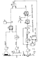
- the current rise detection device 7 which is connected to an amplifier 21 and serves to form the current rise measured value MDI1DT of the branch current i1, can be seen.
- the value MDI1DT is fed to the x input of a comparator 22.
- the voltage detection device 16 for measuring the DC link voltage UZK is designed, for example, as a voltage divider (two resistors 161, 162 are arranged between the poles 2, 3), the voltage divider tap (common connection point of both resistors 161, 162) being connected to an amplifier 23 to which the DC link DC voltage measurement value MUZK can be removed on the output side.
- This value MUZK is divided in a computing unit 24 by LK and multiplied by A, LK representing the total commutation inductance of a phase and A representing a predeterminable evaluation factor between 0 and 1.
- the factor A / LK is "calibrated" in practice in the amplification of the amplifier 23, so that the additional arithmetic unit 24 is only shown for clarification.
- the expression MUZK ⁇ A / LK is applied to the y input of comparator 22.
- the comparator 22 always issues a short-circuit message KM when the value of the signal at the x input exceeds the value of the signal at the y input, ie when MDI1DT is greater than MUZK ⁇ A / LK.
- the short-circuit message kM becomes one in Short-circuit protection device 25 which is of no further interest in this connection and is fed to the first input of an OR gate 26.
- the current detection device 13 measuring the load current iph1 is connected to an amplifier 27.
- the load current measurement value MIPH1 which can be taken from the amplifier 27, is fed to a control device 28, a differentiating element 29 and an addition point 31, which are of no further interest in this context.
- the load current rise measured value MDIPH1Dt which can be derived from the differentiator 29, is multiplied by TS with the aid of a multiplier 30, TS representing the maximum storage time of a GTO thyristor.
- the multiplicative constant factor TS is in practice suitably "calibrated" in the differentiator 29, so that the additional multiplier 30 is only shown for clarification.
- the addition point 31 adds the values MIPH1 and MDIPH1DT ⁇ TS and supplies the sum formed to an amount generator 32.
- is the x'-input of a comparator 33.
- the y'-input of this comparator 33 is subjected to SITQ, the maximum periodically switchable anode current of a GTO thyristor.
- SITQ is e.g. easily adjustable at the tap of a potentiometer 34 connected between a positive voltage and ground.
- the comparator 33 always gives a predictive erase lock LSP to the second input of the OR gate 26 when the value of the signal at the x'-input exceeds the value of the signal at the y'-input, ie when
- the OR gate 26 outputs an erase lock signal LS to a control device 35 Ignition and deletion of the GTO thyristors, whereupon the corresponding GTO thyristors V11 and V12 are not deleted even if the control device 35 is sent corresponding delete signals from the control device 28.
- control device 35 is connected on the output side to the control connections of all GTO thyristors V11 ... V32 and on the input side signals both from the control device 28 and from the OR gate 26 (or from the further OR gates ) of the evaluation electronics.
- the control device 28 receives u. a. Load current measured values MIPH1 .... MIPH3 and forms the appropriate ignition and extinguishing signals for the individual GTO thyristors.
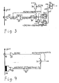
- FIG. 3 shows a first variant of the evaluation electronics.
- the amount of the sum MIPH1 + MDIPH1DT ⁇ TS formed by the addition point 31 is dispensed with, ie the amount generator 32 according to FIG. 2 is omitted.
- the sum MIPH1 + MDIPH1DT ⁇ TS for the GTO thyristors V11, V21, V31 carrying the current from the DC link to the load is directly a first comparator 331 and the sum inverted via an inverter 36 - (MIPH1 + MDIPH1DT ⁇ TS) for the Current from the load to the DC link GTO thyristors V12, V22, V32 fed to a second comparator 332.
- the comparators 331, 332 each have SITQ, the maximum periodically switchable anode current of a GTO, as the second input variable. On the output side, the comparators 331, 332 feed the predictive erase lock LSP to the OR gate 26. The rest of the arrangement is as described under Fig. 2.
- FIG. 4 shows a second variant of the evaluation electronics.
- the derivation of the signal MIPH1 by the differentiator 29 is dispensed with.
- a current rise detection device 18, indicated by dashed lines in FIG. 1 is used, which outputs the load current rise measured value MDIPH1DT via a downstream amplifier 37.
- This value multiplied by the storage time TS is fed to the addition point 31, which, on the other hand, is applied to the load current measurement value MIPH1 formed by the arrangement of the current detection device 13 / amplifier 27. The rest of the arrangement is as described under Fig. 2.
- an extinguishing block signal is a protective measure to counteract the damaging consequences of overcurrents in the GTO thyristors of a converter.
- the causes of the overcurrents can be divided into three main cases.
- the power section of the converter itself is OK.
- Incorrect control of the converter (e.g. as a result of inadequate tax laws or errors in the Control technology), however, excessive load currents occur.
- both the power section and the control system of the converter are OK.
- the load (motor) or the connecting cables between the converter and the load are faulty.
- the first rule is that an erase inhibit signal LS is issued when the amount of the sum of the current load current of the phase and the product of its time derivative (current increase) and the maximum storage time of a GTO thyristor is greater than the permissible switch-off capacity of the GTO -Thyristor is.
- the deletion lock is activated when iph + diph / dt ⁇ TS is larger than ITQ.
- the slope (time derivative) of the load current diph / dt can be obtained, for example, by electronic differentiation (differentiator 29) from the measured value of the load current (alternative: see FIG. 4).
- the accuracy of the diph / dt signal among other things, not very large at high di / dt values.
- the di / dt signal can be both limited and smoothed.
- the extinguishing block In the event of an internal short circuit (third case), the extinguishing block must prevent attempts to switch off the overloaded GTO thyristors until the actual short circuit detection (short circuit protection device 25) triggers protective ignition.
- the short-circuit protection device 25 is activated by the short-circuit message KM, but this must be delayed, filtered and evaluated in order to avoid unnecessary protective ignitions. Protective ignition is therefore delayed. If there is an internal short circuit, the predictive effect of the extinguishing block is not required. The fact of the short circuit as such is sufficient as a trigger criterion.
- the activation according to the first rule is ineffective in the event of an internal short circuit, since the short circuit current does not flow through the output current transformers (current detection devices 13 to 15). Therefore, the existing "fast" unfiltered short-circuit message KM is used to trigger the deletion block.
- the second rule is that an erase inhibit signal LS is issued when the unfiltered short-circuit message KM of the phase is present.
- the short-circuit message is then issued when the current steepness of the branch current, measured with the phase rise detection device of the phase, exceeds a predeterminable threshold value which is in principle proportional to the current intermediate circuit DC voltage UZK of the converter.
- the deletion lock is activated when di / dt is greater than UZK ⁇ A / LK.
- both GTO thyristors conducts at any time in a converter phase. Only in the event of an internal short circuit or a protective firing do both GTO thyristors in a line conduct at the same time. In these special cases, both GTO thyristors also need an extinguishing lock. An erase inhibit signal acting on both GTO thyristors of one phase is therefore sufficient.
- the trigger criteria for the extinguishing block must be equally suitable for both GTO thyristors in one phase. This is the case with the short-circuit message KM. In the case of a predictive delete lock according to the first rule, this is ensured by the amount formation (amount generator 32).
- the third rule is that a single quench inhibit signal LS acts on both GTO thyristors of a bridge phase (string).
- the steepness of the load currents diph / dt never exceeds a limit value G1 when the load circuit is free of defects.
- This limit value G1 can be determined solely from the machine data of the load 17.
- the load currents of the traction inverter essentially expose themselves with a fault-free load circuit the "actual" machine currents and the currents over the winding capacities of the machine together.
- the steepness of the "actual" machine currents is determined by the leakage inductance of the machine in connection with the DC link voltage UZK of the converter and the current EMF (induced electromotive force) of the machine. For example, it is a maximum of 5A / ⁇ s.
- the steepness of the currents over the winding capacity of the machine usually does not exceed 5A / ⁇ s either.
- the limit value G1 can thus be selected to be 10 A / ⁇ s, for example. Since the limit value G1 is so small, the size iph + diph / dt ⁇ TS required for the extinguishing block can be estimated replaced by the size iph + G1 ⁇ TS without reducing the utilization of the converter.
- the extinguishing block is therefore activated with a fault-free load circuit and a suitable drive if iph + G1 ⁇ TS is greater than ITQ, the load current rise measured value being replaced by a "worst-case value" G1.
- the extinguishing block can be triggered if diph / dt is greater than a limit value G2, the limit value G2 being greater than the limit value G1, but clearly below the threshold value relevant for the short-circuit protection device 25.
- a typical limit value G2 is e.g. 25 A / ⁇ s.
- ⁇ G2 are to be replaced, whereby both criteria have to be linked in the sense of an OR link.
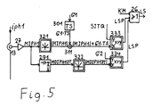
- This fourth variant of the evaluation electronics is shown in FIG. 5.
- the addition point 311 receives the amount of the load current measured value
- + G1 ⁇ TS passes to the comparator 333.
- the comparator 333 outputs a predictive erase lock LSP to the OR gate 26 if the sum
- the load current rise measured value MDIPH1DT which is formed from the load current measured value MIPH1 by means of a differentiating element 291, reaches the comparator 334 via the amount generator 322.
- the comparator 334 outputs a predictive deletion lock LSP to the OR gate 26 if the amount
- the rest of the arrangement is as described under Fig. 2.
Landscapes
- Engineering & Computer Science (AREA)
- Power Engineering (AREA)
- Inverter Devices (AREA)
- Rectifiers (AREA)
Applications Claiming Priority (4)
| Application Number | Priority Date | Filing Date | Title |
|---|---|---|---|
| DE3929861 | 1989-09-08 | ||
| DE3929861 | 1989-09-08 | ||
| DE3934044A DE3934044A1 (de) | 1989-09-08 | 1989-10-12 | Verfahren und vorrichtung zur bildung eines loeschsperrsignals fuer abschaltbare leistungshalbleiter |
| DE3934044 | 1989-10-12 |
Publications (2)
| Publication Number | Publication Date |
|---|---|
| EP0416488A2 true EP0416488A2 (fr) | 1991-03-13 |
| EP0416488A3 EP0416488A3 (en) | 1991-04-24 |
Family
ID=25884895
Family Applications (1)
| Application Number | Title | Priority Date | Filing Date |
|---|---|---|---|
| EP19900116824 Withdrawn EP0416488A3 (en) | 1989-09-08 | 1990-09-01 | Method and means for provinding a turn-off blocking signal for a turn-off power semiconductor device |
Country Status (5)
| Country | Link |
|---|---|
| US (1) | US5053940A (fr) |
| EP (1) | EP0416488A3 (fr) |
| AU (1) | AU6100290A (fr) |
| DE (1) | DE3934044A1 (fr) |
| NO (1) | NO903890L (fr) |
Cited By (3)
| Publication number | Priority date | Publication date | Assignee | Title |
|---|---|---|---|---|
| EP0482504A1 (fr) * | 1990-10-23 | 1992-04-29 | ABBPATENT GmbH | Méthode de protection de semi-conducteurs de puissance à extinction commandable dans un onduleur lors de court-circuits de sortie |
| WO1994003523A1 (fr) * | 1992-08-03 | 1994-02-17 | Henkel Kommanditgesellschaft Auf Aktien | Procede permettant de modifier des polymeres |
| US9285135B2 (en) | 2010-03-16 | 2016-03-15 | Siemens Schweiz Ag | Method for regulating room comfort variables |
Families Citing this family (5)
| Publication number | Priority date | Publication date | Assignee | Title |
|---|---|---|---|---|
| DE69210940T2 (de) * | 1991-10-21 | 1996-11-14 | Toshiba Kawasaki Kk | Leistungsumrichter |
| JP2940843B2 (ja) * | 1992-01-23 | 1999-08-25 | 三菱電機株式会社 | 過電流保護方法及びその装置及び過電流検出装置 |
| JPH07298627A (ja) * | 1994-04-27 | 1995-11-10 | Toshiba Corp | 電力変換器の制御装置 |
| JP2000139085A (ja) * | 1998-08-24 | 2000-05-16 | Shibafu Engineering Kk | 電力変換装置 |
| US10879652B2 (en) | 2018-09-21 | 2020-12-29 | Infineon Technologies Ag | Auxiliary power outlet with load inductance measurement system |
Family Cites Families (7)
| Publication number | Priority date | Publication date | Assignee | Title |
|---|---|---|---|---|
| US4597038A (en) * | 1984-07-26 | 1986-06-24 | Westinghouse Electric Corp. | Switching overlap protection by control gate impedance monitoring |
| DE3434607A1 (de) * | 1984-09-18 | 1986-03-27 | Siemens AG, 1000 Berlin und 8000 München | Verfahren und vorrichtung zum betreiben eines abschalthyristors |
| JPH0753037B2 (ja) * | 1985-01-26 | 1995-06-05 | 株式会社日立製作所 | インバータの保護装置 |
| US4641231A (en) * | 1985-12-06 | 1987-02-03 | General Electric Company | Apparatus and method for failure testing of a control turn-off semiconductor |
| DE3727996A1 (de) * | 1987-08-22 | 1989-03-02 | Asea Brown Boveri | Verfahren und vorrichtung zur unterdrueckung von unzulaessigen loeschversuchen bei abschaltbaren leistungshalbleitern |
| US4775925A (en) * | 1987-11-23 | 1988-10-04 | General Electric Company | Method and apparatus for determining the control electrode to cathode junction voltage of a control turn-off semiconductor device and use of such determined voltage in the control of the device |
| EP0328941A1 (fr) * | 1988-02-16 | 1989-08-23 | Siemens Aktiengesellschaft | Procédé et dispositif de commutation du courant entre des valves déconnectables dans un redresseur de courant |
-
1989
- 1989-10-12 DE DE3934044A patent/DE3934044A1/de not_active Withdrawn
-
1990
- 1990-08-14 AU AU61002/90A patent/AU6100290A/en not_active Abandoned
- 1990-09-01 EP EP19900116824 patent/EP0416488A3/de not_active Withdrawn
- 1990-09-06 NO NO90903890A patent/NO903890L/no unknown
- 1990-09-07 US US07/579,047 patent/US5053940A/en not_active Expired - Fee Related
Cited By (3)
| Publication number | Priority date | Publication date | Assignee | Title |
|---|---|---|---|---|
| EP0482504A1 (fr) * | 1990-10-23 | 1992-04-29 | ABBPATENT GmbH | Méthode de protection de semi-conducteurs de puissance à extinction commandable dans un onduleur lors de court-circuits de sortie |
| WO1994003523A1 (fr) * | 1992-08-03 | 1994-02-17 | Henkel Kommanditgesellschaft Auf Aktien | Procede permettant de modifier des polymeres |
| US9285135B2 (en) | 2010-03-16 | 2016-03-15 | Siemens Schweiz Ag | Method for regulating room comfort variables |
Also Published As
| Publication number | Publication date |
|---|---|
| NO903890D0 (no) | 1990-09-06 |
| NO903890L (no) | 1991-03-11 |
| EP0416488A3 (en) | 1991-04-24 |
| US5053940A (en) | 1991-10-01 |
| AU6100290A (en) | 1991-03-14 |
| DE3934044A1 (de) | 1991-03-21 |
Similar Documents
| Publication | Publication Date | Title |
|---|---|---|
| DE3036619C2 (de) | Schaltungsanordnung für den Kurzschlußschutz von Transistoren | |
| EP3257147B1 (fr) | Ensemble convertisseur et procédé de protection contre les court-circuits dudit ensemble convertisseur | |
| DE2914313A1 (de) | Fehlerstrom-begrenzungsschaltung | |
| DE112011103585T5 (de) | Stromumformervorrichtung | |
| EP0571644A1 (fr) | Procédé et dispositif de delestage d'un condensateur dans un compensateur série commandé en fonction de la charge de son shunt de protection | |
| DE3640546C2 (fr) | ||
| DE69112908T2 (de) | Verfahren und Vorrichtung zum Schutz von Thyristoren. | |
| DE2349161A1 (de) | Anordnung zum schutz eines von einem gleichspannungszwischenkreis gespeisten selbstgefuehrten wechselrichters | |
| DE3040577C2 (fr) | ||
| DE2114284A1 (de) | Selbstregulierter Gleichstrom-Gleichstrom-Konverter | |
| EP0416488A2 (fr) | Méthode et dispositif fournissant un signal de blocage de coupure pour un semi-conducteur de puissance à extinction | |
| DE3338301C2 (fr) | ||
| DE3405793A1 (de) | Verfahren und vorrichtung zum kurzschlussschutz eines stromrichtergeraetes mit gto-thyristoren | |
| DE1488859B2 (de) | Schutzeinrichtung für Asynchronmotoren speisende Wechselrichter | |
| DE4403008A1 (de) | Stromrichteranlage mit Überspannungsschutzschaltung | |
| DE3033916C2 (fr) | ||
| DE3015161C2 (de) | Zwischenkreisumrichter | |
| DE60132418T2 (de) | Verfahren und System zur Nullstrompegeldetektion in einem netzseitig-kommutierten Umrichter | |
| DE2355603A1 (de) | Schutzschaltung | |
| DE3442607C2 (fr) | ||
| DE3512834C2 (fr) | ||
| DE2856268C2 (de) | Schutzeinrichtung für eine Gleichrichterschaltung | |
| DE2724815A1 (de) | Drehzahlregler fuer einen universalmotor | |
| AT404414B (de) | Thyristorschutz durch wechselrichterkipperkennung | |
| EP0482504B1 (fr) | Méthode de protection de semi-conducteurs de puissance à extinction commandable dans un onduleur lors de court-circuits de sortie |
Legal Events
| Date | Code | Title | Description |
|---|---|---|---|
| PUAI | Public reference made under article 153(3) epc to a published international application that has entered the european phase |
Free format text: ORIGINAL CODE: 0009012 |
|
| PUAL | Search report despatched |
Free format text: ORIGINAL CODE: 0009013 |
|
| AK | Designated contracting states |
Kind code of ref document: A2 Designated state(s): AT DE DK IT NL SE |
|
| AK | Designated contracting states |
Kind code of ref document: A3 Designated state(s): AT DE DK IT NL SE |
|
| 17P | Request for examination filed |
Effective date: 19910523 |
|
| 17Q | First examination report despatched |
Effective date: 19930422 |
|
| STAA | Information on the status of an ep patent application or granted ep patent |
Free format text: STATUS: THE APPLICATION IS DEEMED TO BE WITHDRAWN |
|
| 18D | Application deemed to be withdrawn |
Effective date: 19941006 |