EP0416532A2 - Dispositif de mémoire à semi-conducteur associé à des portes logiques ayant un mode opératoire de diagnostic "scan-path" - Google Patents
Dispositif de mémoire à semi-conducteur associé à des portes logiques ayant un mode opératoire de diagnostic "scan-path" Download PDFInfo
- Publication number
- EP0416532A2 EP0416532A2 EP90116966A EP90116966A EP0416532A2 EP 0416532 A2 EP0416532 A2 EP 0416532A2 EP 90116966 A EP90116966 A EP 90116966A EP 90116966 A EP90116966 A EP 90116966A EP 0416532 A2 EP0416532 A2 EP 0416532A2
- Authority
- EP
- European Patent Office
- Prior art keywords
- signal
- write
- circuit
- address
- logic gates
- Prior art date
- Legal status (The legal status is an assumption and is not a legal conclusion. Google has not performed a legal analysis and makes no representation as to the accuracy of the status listed.)
- Withdrawn
Links
Images


Classifications
-
- G—PHYSICS
- G01—MEASURING; TESTING
- G01R—MEASURING ELECTRIC VARIABLES; MEASURING MAGNETIC VARIABLES
- G01R31/00—Arrangements for testing electric properties; Arrangements for locating electric faults; Arrangements for electrical testing characterised by what is being tested not provided for elsewhere
- G01R31/28—Testing of electronic circuits, e.g. by signal tracer
- G01R31/317—Testing of digital circuits
- G01R31/3181—Functional testing
- G01R31/3185—Reconfiguring for testing, e.g. LSSD, partitioning
- G01R31/318533—Reconfiguring for testing, e.g. LSSD, partitioning using scanning techniques, e.g. LSSD, Boundary Scan, JTAG
- G01R31/318555—Control logic
-
- G—PHYSICS
- G11—INFORMATION STORAGE
- G11C—STATIC STORES
- G11C29/00—Checking stores for correct operation ; Subsequent repair; Testing stores during standby or offline operation
- G11C29/04—Detection or location of defective memory elements, e.g. cell constructio details, timing of test signals
- G11C29/08—Functional testing, e.g. testing during refresh, power-on self testing [POST] or distributed testing
- G11C29/12—Built-in arrangements for testing, e.g. built-in self testing [BIST] or interconnection details
- G11C29/18—Address generation devices; Devices for accessing memories, e.g. details of addressing circuits
- G11C29/30—Accessing single arrays
- G11C29/32—Serial access; Scan testing
-
- G—PHYSICS
- G11—INFORMATION STORAGE
- G11C—STATIC STORES
- G11C29/00—Checking stores for correct operation ; Subsequent repair; Testing stores during standby or offline operation
- G11C29/52—Protection of memory contents; Detection of errors in memory contents
Definitions
- This invention relates to a semiconductor memory device associated with peripheral logic gates and, more particularly, to a write-in controlling circuit of the semiconductor memory device responsive to a write enable signal for allowing the peripheral logic gates to rewrite a piece of data information memorized in the memory cell array.
- the semiconductor memory device is of the bipolar SRAM (Static Random Access Memory Device) and comprises a memory cell array MCA for bits of data information associated with peripheral circuits.
- the peripheral circuits include an address latching circuit ALT providing a temporal storage for an address signal ADD, an address decoder circuit DEC selecting an accessible memory cell from the memory cell array MCA, a sense amplifier circuit SA for quick decision of the logic level of a data bit to be read out from the accessible memory cell, and an output buffer circuit OUT producing an output data signal Dout on the basis of the data bit.
- the peripheral circuits further comprise an input buffer circuit DIB for an input data signal Din, a write-in amplifier circuit WA responsive to a write-in controlling signal Wp ′ and supplying an input data bit and the complementary data bit thereof to an accessible memory cell, and a write-in controlling circuit WCL responsive to a write enable signal WE and producing the write-in controlling signal Wp ′.
- the write-in controlling circuit WCL has a latching circuit LT, three delay circuits DLY1, DLY2 and DLY3 and a NAND gate NA.
- the semiconductor memory device thus arranged is associated with peripheral logic gates (not shown) which form flip flop circuits for producing the address signal, the write enable signal WE and the input data signal Din.
- peripheral logic gates are hereinbelow referred to as "logic gate array”.
- the clock signal CLK is delayed by the delay circuit DLY, and the write enable signal WE of the active low level is latched in the latching circuit LT in the presence of the delayed clock signal fed from the delay circuit DLY1.
- the latching circuit LT produces an output signal A complementary to the write enable signal WE but a time delay is introduced in production of the output signal A due to the delay circuit DLY1.
- the latching circuit LT further produces an output signal B in phase with the write enable signal WE but a further time delay is introduced therein due to the delay circuit DLY2.
- the output signal A is NANDed with the output signal B, and the NAND gate NA yields the write-in controlling signal Wp ′ of an active low level at time t2.
- the write-in amplifier circuit WA supplies a data bit and the complementary data bit to the data path in the presence of the write-in controlling signal Wp ′, and the data bit is written into the memory cell.
- the write-in controlling signal Wp ′ is recovered to the inactive high level at time t3, because the delay circuit DLY2 shifts the output signal B to the high level.
- the delay circuit DLY3 introduces a time delay Tset into a propagation of the output signal B, and the output signal thus delayed returns to the latching circuit LT at time t4. Then, the latching circuit LT is reset for the subsequent write-in request.
- a set-up time Tsa is defined by the delay circuit DLY1, and the write-in controlling signal Wp ′ continues to be in the active low level for a time period Tw.
- a memory cycle Tcyc is equivalent to each pulse period of the clock signal CLK.
- the logic gate array is subjected to a diagnosis, and one of the simple diagnoses is known as "scan-path method".
- scan-path diagnostic mode of operation the flip flop circuits in the peripheral logic gate array are coupled as if they form shift registers propagating a testing bit pattern.
- the peripheral logic gate array produces the address signal ADD, the write enable signal WE and the input data signal Din on the basis of the testing bit pattern.
- the address signal ADD, the write enable signal WE and the input data signal Din thus produced in the scan-path diagnostic mode of operation are supplied to the address latching circuit ALT, the latching circuit LT and the input data buffer circuit DIB, respectively, as similar to the usual data write-in mode of operation.
- a problem is encountered in the prior art semiconductor memory device in that a piece of data information memorized in the memory cell is destroyed by the data bit produced on the basis of the input data signal Din during the scan-path diagnostic mode of operation.
- the present invention proposes to prohibit a write-in controlling circuit from supplying a write-in controlling signal to a memory cell array during in a scan-path diagnostic mode of operation.
- a semiconductor memory device associated with peripheral logic gates producing at least an address signal representative of an address, a write enable signal and an input data signal indicative of a piece of data information, the peripheral logic gates selectively entering an usual mode of operation and a scan-path diagnostic mode of operation, comprising: a) a memory cell array having a plurality of memory cells each having an address and memorizing a piece of data information, and b) peripheral circuits having a write-in controlling circuit responsive to the write enable signal and supplying a write-in controlling signal to the memory cell array for allowing a piece of data information indicated by the input data signal to be memorized in one of the memory cells designated by the address signal, in which the peripheral circuits further has a prohibiting circuit operative to prohibit the write-in controlling circuit from supplying the write-in controlling signal in the scan-path diagnostic mode of operation.
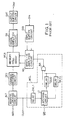
- a semiconductor memory device 100 embodying the present invention is provided in association with peripheral logic gates 101 and comprises a memory cell array 100a having a plurality of memory cells MC11, MC1n, MCm1 and MCmn and various peripheral circuits.
- the memory cells MC11, MCm1, MC1n and MCmn memorize pieces of data information, respectively.
- each of the memory cells MC11, MC1n, MCm1 and MCmn is implemented by bipolar transistors, and is of the SRAM cell.
- the memory cells MC11, MC1n, MCm1 and MCmn may have another memory cell structure.
- the peripheral circuits include an address latching circuit 100b responsive to a clock signal CLK and providing a temporal storage for an address signal ADD fed from the peripheral logic gates 101, an address decoder circuit 100c for designating one of the memory cells MC11, MCm1, MC1n and MCmn, a sense amplifier circuit 100d for the piece of data information read out from one of the memory cells MC11, MCm, MC1n and MCmn designated by the address signal ADD, and an output buffer circuit 100e for producing an output data signal Dout on the basis of the piece of data information.
- These circuits 100b, 100c, 100d and 100e participate a read-out mode of operation.
- the peripheral circuits further include an input buffer circuit 100f supplied with an input data signal Din from the peripheral logic gates 101, and a write-in amplifier circuit 100g responsive to a write-in controlling signal Wp and supplying a data bit and the complementary data bit to one of the memory cells designated by the address signal ADD.
- a prohibiting circuit 100h and a write-in controlling circuit 100i are further incorporated in the peripheral circuits, and the circuits 100b, 100c, 100f, 100g, 100h and 100i participate a write-in mode of operation.
- the write-in controlling circuit 100i is similar to that of the prior art semiconductor memory device, and no further description is incorporated for the sake of simplicity.
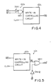
- the arrangement of the prohibiting circuit 100h is illustrated in Fig. 4 in detail.
- the prohibiting circuit 100h comprises a two-input NAND gate NA11 and an inverter circuit INV11 coupled to one of the input nodes of the NAND gate NA11.
- the write enable signal WE is supplied from the peripheral logic gates 101 to the inverter circuit INV11.
- a mode signal SE is supplied to the other input node of the NAND gate NA11, and the mode signal SE of a low level is indicative of a scan-path diagnostic mode of operation.
- the mode signal SE remains in a high level in so far as the peripheral logic gates 101 is in an usual mode of operation.
- the prohibiting circuit 100h propagates the write enable signal WE fed from the peripheral logic gates 101 in the absence of the mode signal SE of the low level; however, the write enable signal WE is blocked by the NAND gate NA in the presence of the mode signal SE of the low level indicative of the scan-path diagnostic mode of operation.
- the prohibiting circuit 100h prohibits the write-in controlling circuit 100i from supplying the write-in controlling signal Wp to the write-in amplifier circuit 100g when the peripheral logic gates 101 enter the scan-path diagnostic mode of operation with the mode signal SE of the low level.
- the peripheral logic gates 101 enter the usual mode of operation and shift the semiconductor memory device 100 between the read-out mode and the write-in mode of operation with the write enable signal WE .
- the write enable signal WE remains in the inactive high level
- the semiconductor memory device 100 allows the peripheral logic gates 101 to access the pieces of data information memorized in the memory cell array 100a, and a piece of data information is read out from one of the memory cells MC11, MCm1, MC1n and MCmn having an address designated by the address signal ADD.
- the write-in controlling signal Wp remains in the inactive high level.
- the address signal ADD indicative of the address assigned to the memory cell is supplied from the peripheral logic gates 101 to the address latching circuit 100b.
- the address signal ADD is latched in the address latching circuit 100b at the trailing edge of the next clock signal CLK as similar to the prior art semiconductor memory device.
- the address signal ADD is decoded by the address decoder circuit 100c, and a data path is established from the write-in amplifier circuit 100g to the memory cell designated by the address signal ADD.
- the peripheral logic gates 101 shifts the write enable signal WE to the active low level, and the prohibiting circuit 100h transfers the write enable signal WE of the active low level to the write-in controlling circuit 100i in the presence of the mode signal SE of the high level.
- the write enable signal WE is latched in the write-in controlling circuit 100i in synchronism with the delayed clock signal CLK, and the write-in controlling signal Wp of the active low level is produced therein as similar to the prior art semiconductor memory device.
- the peripheral logic gates 101 further supplies the input data signal Din representative of a new piece of data information to the input buffer circuit 100f, and a data bit and the complementary data bit is produced therein on the basis of the input data signal Din. While the write-in controlling signal Wp is in the active low level, the data bit and the complementary data bit are transferred from the input buffer circuit 100f to the memory cell array 100a, and the new piece of data information is memorized in the memory cell designated by the address signal ADD. Thus, the memory cells MC11, MCm1, MC1n and MCmn are accessible from the peripheral logic gates 101 as long as the mode signal SE indicates the usual mode of operation.
- the NAND gate NA11 continues to yield the high level signal regardless of the write enable signal WE .
- the output signal in the inactive high level causes the write-in controlling circuit 100i to shift the write-in controlling signal Wp in the inactive high level at all times, and, for this reason, no data write-in operation is carried out even if the input data signal Din and the address signal ADD are fed to the semiconductor memory device 100 in the scan-path diagnostic mode of operation.
- the memory cells MC11, MCm1, MC1n and MCmn are free from any destruction of the pieces of data information which have been already memorized in the usual mode of operation.
- FIG. 5 of the drawings another prohibiting circuit 110h according to the present invention comprises a two-input NOR gate NR11 and an inverter circuit INV12 coupled to one of the input nodes of the NOR gate NR11.
- the prohibiting circuit 110h is incorporated to a semiconductor memory device embodying the present invention, but the other component circuits thereof are similar to those of the first embodiment with the exception that the write-in amplifier circuit 100g transfers the data bit and the complementary data bit in the presence of the write-in controlling signal Wp ⁇ of the active high level. For this reason, detailed description on the other component circuits is omitted for the sake of simplicity.
- the prohibiting circuit 100h is inserted between the peripheral logic gates 101 and the write-in controlling circuit 100i; however, the prohibiting circuit 110h is inserted between the write-in controlling circuit 100i and the write-in amplifier circuit 100g. If the peripheral logic gates 101 enter the usual mode of operation with the mode signal SE of the high level, the inverter circuit INV2 supplies an output signal of the low level, and the NOR gate NR11 serves as an inverter circuit.
- the write-in controlling circuit 100i produces the write-in controlling signal Wp of the inactive high voltage signal, and, accordingly, the NOR gate supplies the write-in controlling signal Wp ⁇ of the inactive low level.
- the write enable signal WE of the active low level results in the write-in controlling signal Wp ⁇ of the active high level.
- the inverter circuit INV2 supplies the high level signal to the NOR gate NR11, and the NOR gate NR11 never responds to the write-in controlling signal Wp .
- the write-in controlling signal Wp ⁇ is fixed to the inactive low level regardless of the write-in controlling signal Wp . In this situation, even though the address signal ADD and the input data signal Din are supplied from the peripheral logic gates 101 during the scan-path diagnostic mode of operation, no data destruction takes place in any memory cell, because the prohibiting circuit 110h blocks the write-in controlling signal Wp .
- the semiconductor memory device is free from any data destruction even if an address signal and an input data signal are fed from the peripheral logic gates in the scan-path diagnostic mode of operation.
Landscapes
- Engineering & Computer Science (AREA)
- General Engineering & Computer Science (AREA)
- Physics & Mathematics (AREA)
- General Physics & Mathematics (AREA)
- Static Random-Access Memory (AREA)
- Techniques For Improving Reliability Of Storages (AREA)
Applications Claiming Priority (2)
| Application Number | Priority Date | Filing Date | Title |
|---|---|---|---|
| JP232113/89 | 1989-09-07 | ||
| JP1232113A JPH0394350A (ja) | 1989-09-07 | 1989-09-07 | 半導体記憶装置 |
Publications (2)
| Publication Number | Publication Date |
|---|---|
| EP0416532A2 true EP0416532A2 (fr) | 1991-03-13 |
| EP0416532A3 EP0416532A3 (en) | 1992-06-24 |
Family
ID=16934211
Family Applications (1)
| Application Number | Title | Priority Date | Filing Date |
|---|---|---|---|
| EP19900116966 Withdrawn EP0416532A3 (en) | 1989-09-07 | 1990-09-04 | Semiconductor memory device associated with peripheral logic gates having a scan-path diagnostic mode of operation |
Country Status (3)
| Country | Link |
|---|---|
| US (1) | US5124946A (fr) |
| EP (1) | EP0416532A3 (fr) |
| JP (1) | JPH0394350A (fr) |
Cited By (1)
| Publication number | Priority date | Publication date | Assignee | Title |
|---|---|---|---|---|
| CN109508303A (zh) * | 2018-09-30 | 2019-03-22 | 中国科学院上海微系统与信息技术研究所 | 一种用于并行数据存储的超导高速缓冲存储器 |
Families Citing this family (4)
| Publication number | Priority date | Publication date | Assignee | Title |
|---|---|---|---|---|
| IL96808A (en) * | 1990-04-18 | 1996-03-31 | Rambus Inc | Introductory / Origin Circuit Agreed Using High-Performance Brokerage |
| US5315549A (en) * | 1991-06-11 | 1994-05-24 | Dallas Semiconductor Corporation | Memory controller for nonvolatile RAM operation, systems and methods |
| US5381369A (en) * | 1993-02-05 | 1995-01-10 | Kabushiki Kaisha Toshiba | Nonvolatile semiconductor memory device using a command control system |
| US7441164B2 (en) * | 2002-12-26 | 2008-10-21 | Broadcom Corporation | Memory bypass with support for path delay test |
Family Cites Families (3)
| Publication number | Priority date | Publication date | Assignee | Title |
|---|---|---|---|---|
| JPS58144954A (ja) * | 1982-02-24 | 1983-08-29 | Fujitsu Ltd | 診断方式 |
| JPS59124091A (ja) * | 1982-12-29 | 1984-07-18 | Fujitsu Ltd | 半導体メモリ |
| JPS6124091A (ja) * | 1984-07-12 | 1986-02-01 | Nec Corp | メモリ回路 |
-
1989
- 1989-09-07 JP JP1232113A patent/JPH0394350A/ja active Pending
-
1990
- 1990-09-04 EP EP19900116966 patent/EP0416532A3/en not_active Withdrawn
- 1990-09-06 US US07/578,111 patent/US5124946A/en not_active Expired - Fee Related
Cited By (2)
| Publication number | Priority date | Publication date | Assignee | Title |
|---|---|---|---|---|
| CN109508303A (zh) * | 2018-09-30 | 2019-03-22 | 中国科学院上海微系统与信息技术研究所 | 一种用于并行数据存储的超导高速缓冲存储器 |
| CN109508303B (zh) * | 2018-09-30 | 2022-12-23 | 中国科学院上海微系统与信息技术研究所 | 一种用于并行数据存储的超导高速缓冲存储器 |
Also Published As
| Publication number | Publication date |
|---|---|
| US5124946A (en) | 1992-06-23 |
| JPH0394350A (ja) | 1991-04-19 |
| EP0416532A3 (en) | 1992-06-24 |
Similar Documents
| Publication | Publication Date | Title |
|---|---|---|
| US5473574A (en) | Multi-port static random access memory with fast write-thru scheme | |
| US7215588B2 (en) | Apparatus for controlling self-refresh period in memory device | |
| US7573778B2 (en) | Semiconductor memory device | |
| EP0954866B1 (fr) | Procedure de controle d'une sdram par un signal d'horloge | |
| US4616344A (en) | Static memory circuit | |
| US4766572A (en) | Semiconductor memory having a bypassable data output latch | |
| KR100328161B1 (ko) | 집적 회로 메모리 | |
| US6061282A (en) | Semiconductor memory having an improved test circuit | |
| US6078527A (en) | Pipelined dual port integrated circuit memory | |
| EP0253161A1 (fr) | Circuit d'essai pour des dispositifs de mémoire à accès direct | |
| KR100338084B1 (ko) | 데이터출력타이밍을 제어하는 회로를 갖는 반도체메모리장치 | |
| US20110317478A1 (en) | Method and Circuit Arrangement for Performing a Write Through Operation, and SRAM Array With Write Through Capability | |
| US5726950A (en) | Synchronous semiconductor memory device performing input/output of data in a cycle shorter than an external clock signal cycle | |
| US6249468B1 (en) | Semiconductor memory device with switching element for isolating bit lines during testing | |
| JP2001028192A (ja) | フラッシュメモリ装置 | |
| US5383155A (en) | Data output latch control circuit and process for semiconductor memory system | |
| EP0416532A2 (fr) | Dispositif de mémoire à semi-conducteur associé à des portes logiques ayant un mode opératoire de diagnostic "scan-path" | |
| EP0325105A1 (fr) | Mémoire multiporte | |
| US6014341A (en) | Synchronous-type semiconductor storage | |
| US6990038B1 (en) | Clock driver and boundary latch for a multi-port SRAM | |
| US6294939B1 (en) | Device and method for data input buffering | |
| EP1784834B1 (fr) | Dispositif de pile de registres et procede a blocage de lecture apres ecriture au moyen de cellules de detection | |
| US20020034102A1 (en) | Semiconductor memory device | |
| KR100340067B1 (ko) | 데이터에 대한 읽기 및 쓰기 동작을 동시에 수행할 수있는 단일 포트 메모리 구조의 메모리 장치 | |
| JPH01116992A (ja) | センス増幅器制御回路 |
Legal Events
| Date | Code | Title | Description |
|---|---|---|---|
| PUAI | Public reference made under article 153(3) epc to a published international application that has entered the european phase |
Free format text: ORIGINAL CODE: 0009012 |
|
| 17P | Request for examination filed |
Effective date: 19900904 |
|
| AK | Designated contracting states |
Kind code of ref document: A2 Designated state(s): DE FR GB |
|
| PUAL | Search report despatched |
Free format text: ORIGINAL CODE: 0009013 |
|
| AK | Designated contracting states |
Kind code of ref document: A3 Designated state(s): DE FR GB |
|
| 17Q | First examination report despatched |
Effective date: 19940531 |
|
| STAA | Information on the status of an ep patent application or granted ep patent |
Free format text: STATUS: THE APPLICATION HAS BEEN WITHDRAWN |
|
| 18W | Application withdrawn |
Withdrawal date: 19941118 |