EP0416645A2 - Plaque de nettoyage pour dispositif de fabrication de semi-conducteurs - Google Patents
Plaque de nettoyage pour dispositif de fabrication de semi-conducteurs Download PDFInfo
- Publication number
- EP0416645A2 EP0416645A2 EP90117281A EP90117281A EP0416645A2 EP 0416645 A2 EP0416645 A2 EP 0416645A2 EP 90117281 A EP90117281 A EP 90117281A EP 90117281 A EP90117281 A EP 90117281A EP 0416645 A2 EP0416645 A2 EP 0416645A2
- Authority
- EP
- European Patent Office
- Prior art keywords
- wafer
- layer
- cleaning plate
- cleaning
- contact faces
- Prior art date
- Legal status (The legal status is an assumption and is not a legal conclusion. Google has not performed a legal analysis and makes no representation as to the accuracy of the status listed.)
- Granted
Links
Images


Classifications
-
- H—ELECTRICITY
- H10—SEMICONDUCTOR DEVICES; ELECTRIC SOLID-STATE DEVICES NOT OTHERWISE PROVIDED FOR
- H10P—GENERIC PROCESSES OR APPARATUS FOR THE MANUFACTURE OR TREATMENT OF DEVICES COVERED BY CLASS H10
- H10P72/00—Handling or holding of wafers, substrates or devices during manufacture or treatment thereof
- H10P72/04—Apparatus for manufacture or treatment
- H10P72/0402—Apparatus for fluid treatment
- H10P72/0406—Apparatus for fluid treatment for cleaning followed by drying, rinsing, stripping, blasting or the like
Definitions
- This invention relates to a cleaning plate for a semiconductor fabricating device, more particularly, it relates to a cleaning plate for cleaning contact faces of components, such as a conveyer, and a hot plate for heating a wafer, etc., in a semiconductor fabricating device contacted with the surfaces of the wafer when it is transferred.
- a cloth moistened with organic solvent such as alcohol is used in order to remove dust which adhere on contact faces of components (such as a conveyer for transferring a wafer, and a hot plate for heating the wafer, etc.) in a semiconductor fabricating device contacted with the surfaces of the wafer when it is transferred.
- the dust can be removed by directly wiping on the contact faces with the cloth.
- the visible dust of more than 100 ⁇ m in diameter can be removed by the use of the above mentioned method. But, the dust of approximately 100 ⁇ m or less in diameter can not be removed with the cloth.
- the dust can be eliminated by contacting between the mirror surface of a wafer for cleaning and the contact faces. In this case, only some dust of 10 ⁇ m in diameter can be take off.
- the contact faces contacted with the wafer is further contaminated.
- a step for cleaning the contact faces is performed repeatedly many times until the contact faces become purity. Thereby, many manufacturing time is required for fabricating the semiconductor device.
- An object of this invention is to provide a cleaning plate for efficiently removing a dust attached on contact faces of components, such as a conveyer, and a hot plate etc., in a semiconductor fabricating device contacted with the surfaces of a wafer when it is transferred.
- a cleaning plate for cleaning the contact faces of the components contacted with the wafer comprises a first layer having the shape equal that of the wafer, and a second layer made up of a fine-grained absorbent formed on at least one of the surface of the first layer.
- the first layer is composed of a wafer and the second layer is made up of a resin having an absorbability of fine dust.
- the first layer is composed of an aluminum plate.
- the first layer comprises a plastic plate and the shape of the cleaning plate of the invention, for example, is equal to a shape of the wafer.
- the cleaning plate of the invention comprises, for example the wafer as the first layer and the fine-grained absorbent as the second layer.
- the second layer is formed on the first layer.
- the cleaning process can be performed by using the transfer process for transferring the wafer without adding a new cleaning process or a new cleaning system for cleaning the contact faces of the components in the semiconductor fabricating device.
- the dust of more than 0.3 ⁇ m in diameter can be removed by using the cleaning plate according to the invention.
- the cleaning plate of this invention When compared to the wafer as the conventional cleaning means, the cleaning plate of this invention has a cleaning ability of twenty two (22) times than that of the conventional cleaning means.
- the frequencies of the cleaning process can be decreased by using the cleaning plate according to the invention.
- a cleaning plate for cleaning contact faces of components such as a conveyer, and a hot plate for heating a wafer, etc.
- components such as a conveyer, and a hot plate for heating a wafer, etc.
- Fig. 1 shows a sectional view of a cleaning plate as a first embodiment of this invention.
- a numerical number 1 denotes a wafer as a first layer of the cleaning plate.
- a numerical number 2 designates a fine-dust absorbability means or absorbent as a second layer. The first layer is covered with the second layer 2.
- the cleaning plate of the embodiment having above mentioned construction was formed by using a spin coating process as shown in Fig. 2.
- the-wafer 1 was installed on the spin-chuck 21.
- the thickness of the wafer 1 was approximately 0.625 mm.
- an absorbent 23 was coated on the wafer 1 from a dispense nozzle 24 keeping a rotation of the spin chuck 21 at 1,000 to 5,000 r.p.m. .
- TSE3033 as a Si absorbent No.1 and TSE3250 as a Si absorbent No.2 are used as the absorbent 23, which are manufactured by TOSHIBA SILICON Corp.
- the spin coating was performed for approximately 30 to 60 seconds.
- the thickness of the absorbent 23 formed by using the spin coating method was less than 1 mm.
- the shape of the cleaning plate 3 was formed as same as that of the wafer transferred on the transfer surface.
- the cleaning plate was dried by keeping it in atmosphere for approximately 30 minutes. Then, the cleaning plate was heated at temperature range of 150 to 160 °C .
- a coating roller 30 instead of the spinner used in the spin coating method could be used for fabricating the absorbent 23 on the wafer 1. In this case, the drying and heating processes after the fabrication of the absorbent 23 on the wafer 1 were performed just as like the spin coating method as described above.
- a dust removable ability of the cleaning plate 3 formed by the above described fabricating process is measured on the contact faces of the components in the semiconductor fabricating device.
- the cleaning method in which the absorbent 2 is transferred on the contact faces of the components is used for the measurement of the dust removable ability.
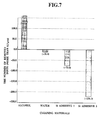
- Fig. 7 is a diagram showing the difference of the dust removable ability between the conventional cleaning plate (only a wafer) and the cleaning plate of the present embodiment.
- the measurement of the dust on the surface of the conveyer is performed with the dust counter WM-II (manufactured by TOKYO KOUGAKU Corp.).
- the vertical line shows the number of dust removed by the cleaning plate and the horizontal line shows the type of cleaning material.
- Si-absorbent 1 Si-adhesive 1
- Si-adhesive 2 Si-adhesive 2
- the dust removable ability of the cleaning plate of the embodiment has about 22 times as high as that of the conventional cleaning plate.
- Dust of less than 0.3 ⁇ m can not be detected by the measurement limitation of the dust counter WM-II
- the cleaning plate comprising the wafer and the absorbent formed on the wafer is disclosed.
- FIg. 4 shows a cross sectional view of a second embodiment of the cleaning plate 40 according to the invention.
- a fine-grained absorbent 41 is covered on the both surface of the wafer 1.
- the shape of the cleaning plate of the second embodiment is formed as same as that of the cleaning plate of the first embodiment.
- the wafer 1 is dipped in a melted absorbent 51 for a predetermined time (the dip method).
- the absorbent is formed on the both surface of the wafer 1.
- the cleaning plate of the third embodiment may be formed only with the absorbent without the wafer.
- Fig. 6 is a sectional diagram of a cleaning plate of a third embodiment according to the invention.
- the cleaning plate 60 is formed only by the absorbent of the second layer as shown in Fig. 4.
- the cleaning plate is fabricated with a rapping plate.
- the shape of the cleaning plate of the third embodiment is formed as same as that of the cleaning plates of the first and second embodiment as shown in Figs. 1 and 4.
- the dust of less than 10 ⁇ m can be eliminated effectively from the transfer surface of the conveyer.
- the wafer as the first layer is used in the first and second embodiments.
- an aluminum plate as a metal plate or a plastic plate as a polymeric material as the first layer can be used for obtaining the same cleaning effect.
- a cleaning plate with a natural rubber, an acrylic resin or a copolymer of an epoxy resin and a nylon as the second layer has the same cleaning ability.
- the second layer is not limited to the type of resin as far as it has the fine-grained absorbability.
- the shape of the cleaning plate is required as same as that of the wafer for most efficiently transferring it on the transfer surface of the conveyer.
- a cleaning plate having another shape for example a perfect disk without an orientation flat, can also be used as far as it can be transferred on the contact faces of the components in the semiconductor fabricating device. This can be used without departing from the scope of the invention.
- the cleaning plate of these embodiment according to the invention can withstand use of several times in cleaning operation for the semiconductor fabricating device.
Landscapes
- Container, Conveyance, Adherence, Positioning, Of Wafer (AREA)
- Cleaning Or Drying Semiconductors (AREA)
- Cleaning In General (AREA)
Applications Claiming Priority (2)
| Application Number | Priority Date | Filing Date | Title |
|---|---|---|---|
| JP23164989A JPH0612784B2 (ja) | 1989-09-08 | 1989-09-08 | 半導体製造装置クリーニング用基体 |
| JP231649/89 | 1989-09-08 |
Publications (3)
| Publication Number | Publication Date |
|---|---|
| EP0416645A2 true EP0416645A2 (fr) | 1991-03-13 |
| EP0416645A3 EP0416645A3 (en) | 1991-04-03 |
| EP0416645B1 EP0416645B1 (fr) | 1998-12-23 |
Family
ID=16926808
Family Applications (1)
| Application Number | Title | Priority Date | Filing Date |
|---|---|---|---|
| EP90117281A Expired - Lifetime EP0416645B1 (fr) | 1989-09-08 | 1990-09-07 | Utilisation d'une plaque de nettoyage pour dispositif de fabrication de semi-conducteurs |
Country Status (4)
| Country | Link |
|---|---|
| EP (1) | EP0416645B1 (fr) |
| JP (1) | JPH0612784B2 (fr) |
| KR (1) | KR930011028B1 (fr) |
| DE (1) | DE69032849T2 (fr) |
Cited By (4)
| Publication number | Priority date | Publication date | Assignee | Title |
|---|---|---|---|---|
| US7713356B2 (en) | 2000-06-06 | 2010-05-11 | Nitto Denko Corporation | Cleaning sheet, conveying member using the same, and substrate processing equipment cleaning method using them |
| US7718255B2 (en) | 2003-08-19 | 2010-05-18 | Nitto Denko Corporation | Cleaning sheets and method of cleaning with the same |
| US7793668B2 (en) | 2000-06-06 | 2010-09-14 | Nitto Denko Corporation | Cleaning sheet, conveying member using the same, and substrate processing equipment cleaning method using them |
| US8460783B2 (en) | 2002-06-19 | 2013-06-11 | Nitto Denko Corporation | Cleaning sheets, transfer member having cleaning function, and method of cleaning substrate-processing apparatus with these |
Families Citing this family (2)
| Publication number | Priority date | Publication date | Assignee | Title |
|---|---|---|---|---|
| AU6368896A (en) * | 1995-07-10 | 1997-02-10 | Precision System Science Co., Ltd. | Measuring instrument |
| JP4557229B2 (ja) * | 2006-05-30 | 2010-10-06 | 日東電工株式会社 | クリーニング機能付搬送部材の製造方法 |
Family Cites Families (6)
| Publication number | Priority date | Publication date | Assignee | Title |
|---|---|---|---|---|
| JPS61124139A (ja) * | 1984-11-21 | 1986-06-11 | Hitachi Ltd | 電子素子の製造方法 |
| JPS61242389A (ja) * | 1985-04-19 | 1986-10-28 | Hitachi Ltd | 電磁記憶デバイスの異物除去方法 |
| JPS61245536A (ja) * | 1985-04-24 | 1986-10-31 | Hitachi Ltd | 電子素子の製造方法 |
| JPS63124531A (ja) * | 1986-11-14 | 1988-05-28 | Hitachi Ltd | 平滑面清掃方法 |
| JPH0695508B2 (ja) * | 1986-11-28 | 1994-11-24 | 大日本スクリ−ン製造株式会社 | 基板の両面洗浄装置 |
| JPH01135574A (ja) * | 1987-11-24 | 1989-05-29 | Osaka Shinku Kogyo Kk | 蒸着薄膜形成用基板の清浄方法 |
-
1989
- 1989-09-08 JP JP23164989A patent/JPH0612784B2/ja not_active Expired - Lifetime
-
1990
- 1990-09-07 DE DE69032849T patent/DE69032849T2/de not_active Expired - Fee Related
- 1990-09-07 KR KR1019900014128A patent/KR930011028B1/ko not_active Expired - Lifetime
- 1990-09-07 EP EP90117281A patent/EP0416645B1/fr not_active Expired - Lifetime
Cited By (4)
| Publication number | Priority date | Publication date | Assignee | Title |
|---|---|---|---|---|
| US7713356B2 (en) | 2000-06-06 | 2010-05-11 | Nitto Denko Corporation | Cleaning sheet, conveying member using the same, and substrate processing equipment cleaning method using them |
| US7793668B2 (en) | 2000-06-06 | 2010-09-14 | Nitto Denko Corporation | Cleaning sheet, conveying member using the same, and substrate processing equipment cleaning method using them |
| US8460783B2 (en) | 2002-06-19 | 2013-06-11 | Nitto Denko Corporation | Cleaning sheets, transfer member having cleaning function, and method of cleaning substrate-processing apparatus with these |
| US7718255B2 (en) | 2003-08-19 | 2010-05-18 | Nitto Denko Corporation | Cleaning sheets and method of cleaning with the same |
Also Published As
| Publication number | Publication date |
|---|---|
| KR910007091A (ko) | 1991-04-30 |
| EP0416645A3 (en) | 1991-04-03 |
| JPH0395951A (ja) | 1991-04-22 |
| DE69032849D1 (de) | 1999-02-04 |
| DE69032849T2 (de) | 1999-06-02 |
| EP0416645B1 (fr) | 1998-12-23 |
| JPH0612784B2 (ja) | 1994-02-16 |
| KR930011028B1 (ko) | 1993-11-19 |
Similar Documents
| Publication | Publication Date | Title |
|---|---|---|
| KR100298632B1 (ko) | 기판부착방법 | |
| EP1391265B1 (fr) | Serviette de nettoyage de contacteur et procede de nettoyage de contacteur | |
| IL90122A (en) | Optically flat surfaces on processed silicon wafers | |
| US5753563A (en) | Method of removing particles by adhesive | |
| US20040083568A1 (en) | Device for cleaning tip and side surfaces of a probe | |
| EP0416645B1 (fr) | Utilisation d'une plaque de nettoyage pour dispositif de fabrication de semi-conducteurs | |
| US20060272676A1 (en) | Cleaning method and a cleaning device for cleaning an edge portion and back face of a wafer | |
| JP3046003B2 (ja) | 電子デバイス用ガラス基板及びその製造方法 | |
| KR100471742B1 (ko) | 세정방법및그것을이용한반도체장치의제조방법 | |
| US6837941B2 (en) | Cleaning and handling methods of electronic component and cleaning apparatus thereof | |
| WO2001031691A1 (fr) | Procede et dispositif de nettoyage de tranche de semi-conducteur | |
| CN213845245U (zh) | 用于竖直地保持半导体晶圆的优化的基板夹持器组件 | |
| JPH07130637A (ja) | 半導体製造装置 | |
| WO2002071461A1 (fr) | Procede de fabrication de semi-conducteurs composes | |
| JP2000260671A (ja) | ダスト吸着用ウエハ及び半導体装置内のクリーニング方法 | |
| US5278104A (en) | Semiconductor wafer carrier having a dust cover | |
| JP3581579B2 (ja) | キャリブレーションウェーハおよびその製造方法 | |
| US5762688A (en) | Particle removal wafer | |
| JPH07148660A (ja) | ウェーハ貼付け方法とウェーハ貼付け装置 | |
| KR20070074398A (ko) | 오염 물질 제거부를 포함하는 반도체 웨이퍼 | |
| EP0410421B1 (fr) | L'utilisation d'un support pour dispositif semi-conducteur | |
| JPS6315250A (ja) | フォトマスク上の粒状物質を減少させる方法およびその装置 | |
| US4588379A (en) | Configuration for temperature treatment of substrates, in particular semi-conductor crystal wafers | |
| US7489494B2 (en) | Guard wafer for semiconductor structure fabrication | |
| JP3362539B2 (ja) | ウェーハの洗浄方法、リンス処理方法及び半導体の製造方法 |
Legal Events
| Date | Code | Title | Description |
|---|---|---|---|
| PUAI | Public reference made under article 153(3) epc to a published international application that has entered the european phase |
Free format text: ORIGINAL CODE: 0009012 |
|
| PUAL | Search report despatched |
Free format text: ORIGINAL CODE: 0009013 |
|
| PUAF | Information related to the publication of a search report (a3 document) modified or deleted |
Free format text: ORIGINAL CODE: 0009199SEPU |
|
| 17P | Request for examination filed |
Effective date: 19900907 |
|
| AK | Designated contracting states |
Kind code of ref document: A2 Designated state(s): DE FR GB |
|
| AK | Designated contracting states |
Kind code of ref document: A3 Designated state(s): DE FR GB |
|
| D17D | Deferred search report published (deleted) | ||
| PUAL | Search report despatched |
Free format text: ORIGINAL CODE: 0009013 |
|
| AK | Designated contracting states |
Kind code of ref document: A3 Designated state(s): DE FR GB |
|
| 17Q | First examination report despatched |
Effective date: 19930621 |
|
| GRAG | Despatch of communication of intention to grant |
Free format text: ORIGINAL CODE: EPIDOS AGRA |
|
| GRAG | Despatch of communication of intention to grant |
Free format text: ORIGINAL CODE: EPIDOS AGRA |
|
| GRAH | Despatch of communication of intention to grant a patent |
Free format text: ORIGINAL CODE: EPIDOS IGRA |
|
| GRAH | Despatch of communication of intention to grant a patent |
Free format text: ORIGINAL CODE: EPIDOS IGRA |
|
| GRAA | (expected) grant |
Free format text: ORIGINAL CODE: 0009210 |
|
| AK | Designated contracting states |
Kind code of ref document: B1 Designated state(s): DE FR GB |
|
| REF | Corresponds to: |
Ref document number: 69032849 Country of ref document: DE Date of ref document: 19990204 |
|
| ET | Fr: translation filed | ||
| PLBE | No opposition filed within time limit |
Free format text: ORIGINAL CODE: 0009261 |
|
| STAA | Information on the status of an ep patent application or granted ep patent |
Free format text: STATUS: NO OPPOSITION FILED WITHIN TIME LIMIT |
|
| 26N | No opposition filed | ||
| REG | Reference to a national code |
Ref country code: GB Ref legal event code: IF02 |
|
| PGFP | Annual fee paid to national office [announced via postgrant information from national office to epo] |
Ref country code: DE Payment date: 20070830 Year of fee payment: 18 |
|
| PGFP | Annual fee paid to national office [announced via postgrant information from national office to epo] |
Ref country code: GB Payment date: 20070905 Year of fee payment: 18 |
|
| PGFP | Annual fee paid to national office [announced via postgrant information from national office to epo] |
Ref country code: FR Payment date: 20070914 Year of fee payment: 18 |
|
| GBPC | Gb: european patent ceased through non-payment of renewal fee |
Effective date: 20080907 |
|
| REG | Reference to a national code |
Ref country code: FR Ref legal event code: ST Effective date: 20090529 |
|
| PG25 | Lapsed in a contracting state [announced via postgrant information from national office to epo] |
Ref country code: DE Free format text: LAPSE BECAUSE OF NON-PAYMENT OF DUE FEES Effective date: 20090401 |
|
| PG25 | Lapsed in a contracting state [announced via postgrant information from national office to epo] |
Ref country code: FR Free format text: LAPSE BECAUSE OF NON-PAYMENT OF DUE FEES Effective date: 20080930 |
|
| PG25 | Lapsed in a contracting state [announced via postgrant information from national office to epo] |
Ref country code: GB Free format text: LAPSE BECAUSE OF NON-PAYMENT OF DUE FEES Effective date: 20080907 |