EP0417295A1 - Element de circuit optique du type guide d'ondes - Google Patents
Element de circuit optique du type guide d'ondes Download PDFInfo
- Publication number
- EP0417295A1 EP0417295A1 EP90901661A EP90901661A EP0417295A1 EP 0417295 A1 EP0417295 A1 EP 0417295A1 EP 90901661 A EP90901661 A EP 90901661A EP 90901661 A EP90901661 A EP 90901661A EP 0417295 A1 EP0417295 A1 EP 0417295A1
- Authority
- EP
- European Patent Office
- Prior art keywords
- mode
- electrodes
- waveguides
- length
- directional coupler
- Prior art date
- Legal status (The legal status is an assumption and is not a legal conclusion. Google has not performed a legal analysis and makes no representation as to the accuracy of the status listed.)
- Granted
Links
- 230000003287 optical effect Effects 0.000 title claims abstract description 57
- 230000008878 coupling Effects 0.000 claims abstract description 43
- 238000010168 coupling process Methods 0.000 claims abstract description 43
- 238000005859 coupling reaction Methods 0.000 claims abstract description 43
- 230000005684 electric field Effects 0.000 claims abstract description 18
- 230000000694 effects Effects 0.000 abstract description 6
- 230000010287 polarization Effects 0.000 abstract description 4
- 238000004891 communication Methods 0.000 abstract description 3
- 239000013307 optical fiber Substances 0.000 abstract description 3
- 239000000758 substrate Substances 0.000 description 15
- 239000010936 titanium Substances 0.000 description 7
- 238000009792 diffusion process Methods 0.000 description 6
- 238000010586 diagram Methods 0.000 description 5
- 239000013078 crystal Substances 0.000 description 4
- 238000004519 manufacturing process Methods 0.000 description 3
- 230000005693 optoelectronics Effects 0.000 description 3
- 229920002120 photoresistant polymer Polymers 0.000 description 3
- 238000010276 construction Methods 0.000 description 2
- 239000002184 metal Substances 0.000 description 2
- 229910052751 metal Inorganic materials 0.000 description 2
- 238000000034 method Methods 0.000 description 2
- 230000005855 radiation Effects 0.000 description 2
- 229910003327 LiNbO3 Inorganic materials 0.000 description 1
- RTAQQCXQSZGOHL-UHFFFAOYSA-N Titanium Chemical compound [Ti] RTAQQCXQSZGOHL-UHFFFAOYSA-N 0.000 description 1
- 230000031700 light absorption Effects 0.000 description 1
- GQYHUHYESMUTHG-UHFFFAOYSA-N lithium niobate Chemical compound [Li+].[O-][Nb](=O)=O GQYHUHYESMUTHG-UHFFFAOYSA-N 0.000 description 1
- 239000003960 organic solvent Substances 0.000 description 1
- 229910052719 titanium Inorganic materials 0.000 description 1
Images





Classifications
-
- G—PHYSICS
- G02—OPTICS
- G02F—OPTICAL DEVICES OR ARRANGEMENTS FOR THE CONTROL OF LIGHT BY MODIFICATION OF THE OPTICAL PROPERTIES OF THE MEDIA OF THE ELEMENTS INVOLVED THEREIN; NON-LINEAR OPTICS; FREQUENCY-CHANGING OF LIGHT; OPTICAL LOGIC ELEMENTS; OPTICAL ANALOGUE/DIGITAL CONVERTERS
- G02F1/00—Devices or arrangements for the control of the intensity, colour, phase, polarisation or direction of light arriving from an independent light source, e.g. switching, gating or modulating; Non-linear optics
- G02F1/29—Devices or arrangements for the control of the intensity, colour, phase, polarisation or direction of light arriving from an independent light source, e.g. switching, gating or modulating; Non-linear optics for the control of the position or the direction of light beams, i.e. deflection
- G02F1/31—Digital deflection, i.e. optical switching
- G02F1/313—Digital deflection, i.e. optical switching in an optical waveguide structure
- G02F1/3132—Digital deflection, i.e. optical switching in an optical waveguide structure of directional coupler type
-
- G—PHYSICS
- G02—OPTICS
- G02F—OPTICAL DEVICES OR ARRANGEMENTS FOR THE CONTROL OF LIGHT BY MODIFICATION OF THE OPTICAL PROPERTIES OF THE MEDIA OF THE ELEMENTS INVOLVED THEREIN; NON-LINEAR OPTICS; FREQUENCY-CHANGING OF LIGHT; OPTICAL LOGIC ELEMENTS; OPTICAL ANALOGUE/DIGITAL CONVERTERS
- G02F2201/00—Constructional arrangements not provided for in groups G02F1/00 - G02F7/00
- G02F2201/12—Constructional arrangements not provided for in groups G02F1/00 - G02F7/00 electrode
- G02F2201/125—Constructional arrangements not provided for in groups G02F1/00 - G02F7/00 electrode delta-beta
-
- G—PHYSICS
- G02—OPTICS
- G02F—OPTICAL DEVICES OR ARRANGEMENTS FOR THE CONTROL OF LIGHT BY MODIFICATION OF THE OPTICAL PROPERTIES OF THE MEDIA OF THE ELEMENTS INVOLVED THEREIN; NON-LINEAR OPTICS; FREQUENCY-CHANGING OF LIGHT; OPTICAL LOGIC ELEMENTS; OPTICAL ANALOGUE/DIGITAL CONVERTERS
- G02F2203/00—Function characteristic
- G02F2203/06—Polarisation independent
Definitions
- This invention relates to waveguide type optical circuit element using a directional coupler, and particularly to a waveguide type optical circuit for use in optical fiber communication, which has an excellent effect of shutting light in optical wave-guides and has reduced polarity-dependence.
- this type of waveguide type optical circuit element includes, as a principal part thereof, a directional coupler as schematically shown in Fig. 10.
- a conventional waveguide type optical circuit element such as a polarity-independent optical switch, has a lithium niobate (LiNb0 3 hereinafter) substrate 1 defining two wave-guides 2 and 3, parts of the waveguides 2 and 3 being close to each other to form a coupling section 6.
- LiNb0 3 lithium niobate
- TE mode refers to a polarization state in which electric field components are parallel to the substrate 1
- TM mode refers to a polarization state in which the electric field components are vertical to the substrate 1. It is to be noted that the two wave-guides 2 and 3 have an identical structure.
- the conventional directional coupler of the polarity-independent optical switch acting as a wave-guide type optical circuit element includes a pair of electrodes (not shown) in the coupling section 6 to be the uniform ⁇ type, and is capable of switching incident light in accordance with the electro-optical effect produced by applying an electric field.
- This switching state is shown in Fig. 11(B) as a uniform ⁇ switching diagram.
- ⁇ state bar state
- PB 0
- the , ⁇ estate appears on a plurality of circular arcs when an electric field ( ⁇ L/ ⁇ ) is applied.
- the conventional polarity-independent optical switch comprising a waveguide type optical circuit element is described in ELECTRONICS LETTERS 8th October 1987 Vol. 23, No. 21, pages 1167-1168, which is shown in Fig. 13.
- the conventional polarity-independent optical switch has a LiNb0 3 substrate 1 defining two waveguides 2 and 3, a pair of electrodes 4 and 5 arranged on the two waveguides 2 and 3, and another pair of electrodes 45 and 55 arranged outwardly of the pair of electrodes 4 and 5.
- Fig. 14 shows the crosstalk of the TE and TM modes for ⁇ (corresponding to the applied voltage) in this case.
- ⁇ ⁇ TE/ ⁇ TM( ⁇ TE, ⁇ TM being phase mismatches of the directional coupler for the TE and TM modes, respectively).
- ⁇ ⁇ TE/ ⁇ TM( ⁇ TE, ⁇ TM being phase mismatches of the directional coupler for the TE and TM modes, respectively).
- ⁇ ⁇ TE/ ⁇ TM( ⁇ TE, ⁇ TM being phase mismatches of the directional coupler for the TE and TM modes, respectively.
- the crosstalk can be made -20dB or less for both modes by adjusting the applied voltage.
- Still another conventional polarity-independent optical switch comprising a waveguide type optical circuit element is described in ELECTRONICS LETTERS 15th September 1988 Vol. 24, No. 19, pages 1198-1200.
- This conventional polarity-independent optical switch secures the polarity independence by using an X-cut crystal which produces the electro-optical effect equally for both the TE and TM modes in the case of an optical crystal such as LiNbO 3 .
- the conventional waveguide type optical circuit element is constructed as noted above, ⁇ L/ ⁇ for mode switching is different between the TE mode and TM mode as shown in the switching diagram of Fig. 12, which has the problem that polarity independence cannot be made perfect.
- an equal complete coupling length for the TE and TM modes is obtained relatively close to a cut-off condition.
- the optical waveguides are thin and produces a weak confinement effect, waveguide propagation loss and radiation loss at curved portions of the wave- guides tend to be large.
- the waveguide type optical circuit element using the X-cut crystal has a weak electro-optical effect available, and therefore has the problem of necessitating a high drive voltage.
- This invention has been made to solve such problems, and its object is to provide a waveguide type optical circuit element which has reduced polarity dependence, provides waveguides that have excellent light confining effect, and requires a reduced drive voltage.
- a directional coupler formed on a waveguide type optical circuit element has a coupling section length which is in a TE mode about three times a complete coupling length of the TE mode, and in a TM mode about one time a complete coupling length of the TM mode.
- electric field applying electrodes formed on the waveguide constituting the directional coupler comprise three-part electrodes which act as reverse A;8 electrodes for alternately reversing a direction of an electric field. This reduces the drive voltage necessary for carrying out an optical switching operation, and realizes optimal element characteristics by varying lengths of the three electrodes in accordance with a ratio of variations in the propagation coefficient in the TE mode and TM mode of the directional coupler manufactured.
- Fig. 1 is a schematic view showing the principle of a waveguide type optical circuit element according to this invention.
- Fig. 2 is a graph of relationship of channel output intensity in (9 state with perfect coupling length.
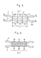
- Fig. 3 is a plan view of an element according to one embodiment of this invention.
- Fig. 4 is a plan view showing the way in which electrodes in the same element are charged.
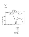
- Fig. 5(A), (B) are graphs showing element characteristics of the element according to this embodiment.
- Fig. 6 is a plan view of an element according to another embodiment of this invention.
- Figs. 7(A), (B), (C) and Figs. 8(A), (B) are graphs showing element characteristics of elements according to different embodiments of this invention.
- FIG. 9(A)-(F) are front views of an element showing a manufacturing process of the element.
- Fig. 10 is a schematic view of a conventional waveguide type optical circuit element.
- Fig. 11 (A) is a graph of relationship of exit light intensity with complete coupling length.
- Fig. 11 (B) is a switching diagram of uniform ⁇ .
- Fig. 12 is a switching diagram of TE and TM modes.
- Fig. 13 is a schematic view of another conventional element.
- Fig. 14 is a view showing a graph of relationship of input loss with switching voltage in the TE mode.
- Fig. 1 is a schematic view, for illustrating the principle of this invention, of polarity-independent optical switch acting as a waveguide type optical circuit element.
- the waveguide type optical circuit element comprises a directional coupler having a LiNb0 3 substrate 1 defining two wave-guides 2 and 3, parts of the waveguides 2 and 3 being close to each other to form a coupling section 6.
- the coupling section 6 has coupling section length L for the TE mode about three times complete coupling length tTE for the TE mode, and for the TN mode about one time complete coupling length t TM for the TM mode.
- Electrodes 4 and 5 for applying a switching voltage V are formed on the waveguides 2 and 3 constituting the coupling section 6 to convert light intensity between the two waveguides 2 and 3.
- FIG. 2 is a light intensity graph showing relationship of channel output intensity in a state with the complete coupling length.
- numerical ranges are defined as 2.7 ⁇ L/lTE ⁇ 3.3 for the TE mode and 0.75 L/lTM ⁇ 1.3 for the TM mode, and these numerical ranges are defined from the view point of input loss.
- these complete coupling lengths are 2.75 L/lTE ⁇ 3.3 and 0.7 ⁇ L/lTM ⁇ 1.3
- the channel output light intensity in o state may have a lower limit at about 75%.
- the complete coupling lengths for the TE and TM modes may be 2.6 ⁇ L/lTE ⁇ 3.4 and 0.6 ⁇ L/lTM ⁇ 1.4.
- Ti (titanium) diffusion is most commonly used as a method of forming the wave-guides 2 and 3 on the LiNb0 3 substrate 1.
- Ti diffusion method it is easy to increase refractive index variation one for extraordinary rays over refractive index variation ⁇ n o for ordinary rays.
- the coupling section length L of the directional coupler By appropriately setting the width of the waveguides 2 and 3, spacing between the two waveguides 2 and 3, and conditions for the Ti diffusion, it is easy to make the coupling section length L of the directional coupler about three times and one time the complete coupling lengths in the TE and TM modes. This allows the wave-guides to be formed thick on the substrate for a sufficient light confinement effect.
- this embodiment has electrodes 4 and 5 divided into three electrodes 11, 12 and 13 acting as reverse ⁇ electrodes for alternately reversing the direction of the electric field. That is, this directional coupler has a coupling section length L, with each of the electrodes 11-13 having a length U3, and an equal voltage of opposite polarity is applied to an adjacent pair of electrodes. This enables a reduction of the drive voltage necessary for an optical switching operation.
- the above directional coupler is manufactured so that the coupling section length L satisfies the relations of 2.7 ⁇ L/lTE ⁇ 3.3 and 0.7 ⁇ L/lTM ⁇ 1.3 with complete coupling lengths TE and TM for the TE mode and the TM mode as already described.
- the waveguides undergo variations in the propagation constant such as + ⁇ , - ⁇ and + ⁇ between the respective divisions as shown in Fig. 3. These propagation coefficient variations differ between the TE mode and TM mode, and the difference is expressed by the following equation:
- Figs. 5(A) and (B) show element characteristics of this embodiment having the electrodes divided into three parts as shown in Figs. 3 and 4.
- the horizontal axis represents ⁇ L/ ⁇ for the TM mode
- the vertical axis represents the power ratio -10Iog(S/Ro) of output light power from wave-guide 3a with intensity S in the TE mode and TM mode with respect to the incident light power of Ro where light power "1 enters the waveguide 2 with intensity Ro and light power "0" enters the waveguide 3.
- the solid lines indicate the light in the TM mode
- the broken lines indicate the light in the TE mode.
- the output light intensities in the TE and TM modes vary in a manner substantially corresponding to variations of ⁇ L/ ⁇ .
- Waveguide type optical circuit elements such as a branching ratio variable optical divider and an information distributing optical switch can be realized by utilizing this characteristic.
- a 3.8 is made with the length of each electrode equally divided into L/3.
- the optimal element characteristic may be obtained by noting the value "a" of the directional coupler manufactured and setting the length of each electrode on the basis of this value.
- Fig. 6 shows a directional coupler designed from the above point of view. It differs from the directional coupler shown in Fig. 3 in that the length of each electrode is not equally divided into L/3 but the length of each is divided into different lengths in accordance with the value of "a".
- the optimal characteristic of an optical switch may be obtained by determining the values of u, v and w after noting the value of a.
- the output intensities of light vary equally with the variations of ⁇ L/ ⁇ for the TM and TE modes.
- the output intensities of light vary equally with the variations of ⁇ L/ ⁇ for the TM and TE modes.
- Figs. 9(A)-(F) show a process of manufacturing the element in this embodiment.
- a photoresist 61 defining waveguide patterns is formed on the Z-cut LiNb0 3 substrate 1 (Fig. 9(A)).
- Ti 62 is deposited as a diffusion source on the substrate 1 having the photoresist 61 (Fig. 9(B)).
- the photoresist 61 is removed from the substrate 1 by using an organic solvent whereby the Ti forms lift-off parts 63 having a width W, a gap G and a height T (Fig. 9(C)).
- the substrate 1 having the lift-off parts 63 of the optical waveguide patterns is heated to a high temperature to spread the Ti acting as the diffusion source, thereby forming the optical waveguides 64 (Fig. 9(D)).
- a Si0 2 film 65 having a thickness of 4000A for example is formed as a buffer layer on the surface of the substrate 1 defining the optical waveguides 64 (Fig. 9(E))
- electrodes 66 are formed on the Si0 2 film 65 above and opposite the optical waveguides 64 (Fig. 9(F)). Since the electrodes 66 comprise a metal, the Si0 2 film 65 is formed in order to avoid light absorption by the metal. In order to satisfy the conditions of the above coupling section, it is necessary to appropriately set the dimensions W, G and T in Fig. 9(C) and conditions for diffusion.
- the waveguide type optical circuit element according to this invention is useful as a polarity-independent optical switch or a variable optical divider for optical fiber communications and the like.
Landscapes
- Physics & Mathematics (AREA)
- Nonlinear Science (AREA)
- General Physics & Mathematics (AREA)
- Optics & Photonics (AREA)
- Optical Integrated Circuits (AREA)
Abstract
Applications Claiming Priority (5)
| Application Number | Priority Date | Filing Date | Title |
|---|---|---|---|
| JP8245889 | 1989-03-31 | ||
| JP82458/89 | 1989-03-31 | ||
| JP1219246A JP2754774B2 (ja) | 1989-03-31 | 1989-08-25 | 導波路型光回路素子 |
| JP219246/89 | 1989-08-25 | ||
| PCT/JP1990/000005 WO1990012341A1 (fr) | 1989-03-31 | 1990-01-04 | Element de circuit optique du type guide d'ondes |
Publications (3)
| Publication Number | Publication Date |
|---|---|
| EP0417295A1 true EP0417295A1 (fr) | 1991-03-20 |
| EP0417295A4 EP0417295A4 (en) | 1992-07-22 |
| EP0417295B1 EP0417295B1 (fr) | 1995-03-08 |
Family
ID=26423468
Family Applications (1)
| Application Number | Title | Priority Date | Filing Date |
|---|---|---|---|
| EP90901661A Expired - Lifetime EP0417295B1 (fr) | 1989-03-31 | 1990-01-04 | Element de circuit optique du type guide d'ondes |
Country Status (5)
| Country | Link |
|---|---|
| US (1) | US5103491A (fr) |
| EP (1) | EP0417295B1 (fr) |
| JP (1) | JP2754774B2 (fr) |
| DE (1) | DE69017564T2 (fr) |
| WO (1) | WO1990012341A1 (fr) |
Cited By (1)
| Publication number | Priority date | Publication date | Assignee | Title |
|---|---|---|---|---|
| EP0646832A3 (fr) * | 1993-10-04 | 1995-12-27 | At & T Corp | Coupleur directionnel delta bêta inversé peu dépendant du procédé de fabrication. |
Families Citing this family (6)
| Publication number | Priority date | Publication date | Assignee | Title |
|---|---|---|---|---|
| FR2668615B1 (fr) * | 1990-10-31 | 1992-12-11 | France Etat | Separateur de polarisations pour lumiere guidee. |
| JPH07318986A (ja) * | 1994-05-25 | 1995-12-08 | Nec Corp | 導波路型光スイッチ |
| US7236708B2 (en) * | 2001-10-25 | 2007-06-26 | Nippon Telegraph And Telephone Corporation | Optical communication system with optical output level control function |
| CN108307658B (zh) * | 2013-09-12 | 2020-11-13 | 罗格斯(新泽西州立)大学 | 高密度光子集成的波导超晶格 |
| JP6662616B2 (ja) * | 2015-11-26 | 2020-03-11 | ダイキョーニシカワ株式会社 | 車両の内装構造 |
| WO2022051021A2 (fr) * | 2020-07-02 | 2022-03-10 | President And Fellows Of Harvard College | Guides d'ondes électromagnétiques utilisant une conversion de mode en cascade |
Family Cites Families (12)
| Publication number | Priority date | Publication date | Assignee | Title |
|---|---|---|---|---|
| US4291939A (en) * | 1978-03-24 | 1981-09-29 | The United States Of America As Represented By The Secretary Of The Navy | Polarization-independent optical switches/modulators |
| US4243295A (en) * | 1979-09-19 | 1981-01-06 | Bell Telephone Laboratories, Incorporated | Polarization-independent optical directional coupler switch/modulator |
| JPS56110916A (en) * | 1980-02-06 | 1981-09-02 | Nec Corp | Magnetic-optical thin film optical switch |
| US4390236A (en) * | 1981-03-19 | 1983-06-28 | Bell Telephone Laboratories, Incorporated | Tunable polarization independent wavelength filter |
| US4679893A (en) * | 1983-08-26 | 1987-07-14 | Hughes Aircraft Company | High switching frequency optical waveguide switch, modulator, and filter devices |
| US4711515A (en) * | 1984-05-29 | 1987-12-08 | American Telephone And Telegraph Company, At&T Bell Laboratories | Electrooptic polarization multiplexer/demultiplexer |
| JPH0785151B2 (ja) * | 1986-06-19 | 1995-09-13 | 富士通株式会社 | 導波路光スイツチ |
| JPS63142333A (ja) * | 1986-12-05 | 1988-06-14 | Oki Electric Ind Co Ltd | 導波型光スイツチ |
| JPH01118821A (ja) * | 1987-11-02 | 1989-05-11 | Oki Electric Ind Co Ltd | 導波型光スイッチ |
| DE3883492T2 (de) * | 1987-11-20 | 1993-12-23 | Ericsson Telefon Ab L M | Verfahren zur Anordnung eines polarisationsrichtenden optoelektronischen Schalters und ein Schalter dafür. |
| US4865408A (en) * | 1989-01-09 | 1989-09-12 | American Telephone And Telegraph Company | Low crosstalk reversed Δβ electrodes for directional coupler switch |
| US4997245A (en) * | 1990-01-04 | 1991-03-05 | Smiths Industries Aerospace & Defense Systems Incorporated | Polarization independent optical switches |
-
1989
- 1989-08-25 JP JP1219246A patent/JP2754774B2/ja not_active Expired - Lifetime
-
1990
- 1990-01-04 DE DE69017564T patent/DE69017564T2/de not_active Expired - Fee Related
- 1990-01-04 US US07/566,460 patent/US5103491A/en not_active Expired - Fee Related
- 1990-01-04 EP EP90901661A patent/EP0417295B1/fr not_active Expired - Lifetime
- 1990-01-04 WO PCT/JP1990/000005 patent/WO1990012341A1/fr not_active Ceased
Non-Patent Citations (3)
| Title |
|---|
| IEEE JOURNAL OF QUANTUM ELECTRONICS vol. QE-13, no. 4, April 1977, pages 122 - 128; R.A.STEINBERG ET AL.: 'DESIGN OF INTEGRATED OPTICAL SWITCHES FOR USE INFIBER DATA TRANSMISSION SYSTEMS' * |
| IEEE JOURNAL OF QUANTUM ELECTRONICS vol. QE-14, no. 8, August 1978, pages 577 - 579; P.S.CROSS ET AL.: 'OPTICALLY CONTROLLED TWO CHANNEL INTEGRATED OPTICAL SWITCH' * |
| See also references of WO9012341A1 * |
Cited By (1)
| Publication number | Priority date | Publication date | Assignee | Title |
|---|---|---|---|---|
| EP0646832A3 (fr) * | 1993-10-04 | 1995-12-27 | At & T Corp | Coupleur directionnel delta bêta inversé peu dépendant du procédé de fabrication. |
Also Published As
| Publication number | Publication date |
|---|---|
| US5103491A (en) | 1992-04-07 |
| JPH037910A (ja) | 1991-01-16 |
| EP0417295A4 (en) | 1992-07-22 |
| DE69017564T2 (de) | 1995-11-02 |
| JP2754774B2 (ja) | 1998-05-20 |
| EP0417295B1 (fr) | 1995-03-08 |
| WO1990012341A1 (fr) | 1990-10-18 |
| DE69017564D1 (de) | 1995-04-13 |
Similar Documents
| Publication | Publication Date | Title |
|---|---|---|
| US4679893A (en) | High switching frequency optical waveguide switch, modulator, and filter devices | |
| KR100261230B1 (ko) | 집적광학 광 강도 변조기 및 그 제조방법 | |
| JP4703627B2 (ja) | 1×2偏波スプリッタおよび1×2偏波無依存型光スイッチ | |
| US7088875B2 (en) | Optical modulator | |
| US4866406A (en) | Wide-band optical modulator | |
| EP1155355B1 (fr) | Reseau de diffraction a reglage electrique | |
| US7522784B2 (en) | Asymmetric directional coupler having a reduced drive voltage | |
| US4983006A (en) | Polarization-independent optical waveguide switch | |
| US4818063A (en) | Optical modulating/switching device | |
| JPH03203716A (ja) | 電気光学変調器 | |
| EP0153312B1 (fr) | Dispositif de filtre électro-optique | |
| EP0417295B1 (fr) | Element de circuit optique du type guide d'ondes | |
| US5679291A (en) | Method of fabricating optical waveguide device | |
| EP1403692A1 (fr) | Dispositifs electro-optique | |
| US6363189B1 (en) | Directional coupler | |
| EP0478226A1 (fr) | Commutateur optique à guides d'ondes | |
| US6374018B1 (en) | Optical switch, method of operating optical switch, and method of designing optical switch | |
| EP0558801B1 (fr) | Dispositif de conversion de longeur d'onde | |
| JPS57158616A (en) | Optical coupler | |
| KR100207599B1 (ko) | 저전압 광스위치 및 그 제조방법 | |
| El-Den et al. | Voltage Controlled-Bandwidth Electrooptic Push-Pull Mach Zehnder Modulator with Coplanar Electrodes | |
| JPH05341243A (ja) | モード変換器及び光フィルタ | |
| Pan et al. | Field-effect electro-optic modulators | |
| Tsao et al. | Combined FD-CM numerical analysis of coplanar electrode waveguide for LiNbO3 automatic polarization controller | |
| JPH02262129A (ja) | 導波路型光スイッチ |
Legal Events
| Date | Code | Title | Description |
|---|---|---|---|
| PUAI | Public reference made under article 153(3) epc to a published international application that has entered the european phase |
Free format text: ORIGINAL CODE: 0009012 |
|
| 17P | Request for examination filed |
Effective date: 19900829 |
|
| AK | Designated contracting states |
Kind code of ref document: A1 Designated state(s): DE FR GB |
|
| A4 | Supplementary search report drawn up and despatched |
Effective date: 19920605 |
|
| AK | Designated contracting states |
Kind code of ref document: A4 Designated state(s): DE FR GB |
|
| 17Q | First examination report despatched |
Effective date: 19930728 |
|
| GRAA | (expected) grant |
Free format text: ORIGINAL CODE: 0009210 |
|
| AK | Designated contracting states |
Kind code of ref document: B1 Designated state(s): DE FR GB |
|
| REF | Corresponds to: |
Ref document number: 69017564 Country of ref document: DE Date of ref document: 19950413 |
|
| ET | Fr: translation filed | ||
| REG | Reference to a national code |
Ref country code: GB Ref legal event code: 746 Effective date: 19951115 |
|
| PLBE | No opposition filed within time limit |
Free format text: ORIGINAL CODE: 0009261 |
|
| STAA | Information on the status of an ep patent application or granted ep patent |
Free format text: STATUS: NO OPPOSITION FILED WITHIN TIME LIMIT |
|
| 26N | No opposition filed | ||
| REG | Reference to a national code |
Ref country code: FR Ref legal event code: D6 |
|
| PGFP | Annual fee paid to national office [announced via postgrant information from national office to epo] |
Ref country code: GB Payment date: 19990107 Year of fee payment: 10 |
|
| PGFP | Annual fee paid to national office [announced via postgrant information from national office to epo] |
Ref country code: DE Payment date: 19990108 Year of fee payment: 10 |
|
| PGFP | Annual fee paid to national office [announced via postgrant information from national office to epo] |
Ref country code: FR Payment date: 19990111 Year of fee payment: 10 |
|
| PG25 | Lapsed in a contracting state [announced via postgrant information from national office to epo] |
Ref country code: GB Free format text: LAPSE BECAUSE OF NON-PAYMENT OF DUE FEES Effective date: 20000104 |
|
| GBPC | Gb: european patent ceased through non-payment of renewal fee |
Effective date: 20000104 |
|
| PG25 | Lapsed in a contracting state [announced via postgrant information from national office to epo] |
Ref country code: FR Free format text: LAPSE BECAUSE OF NON-PAYMENT OF DUE FEES Effective date: 20000929 |
|
| PG25 | Lapsed in a contracting state [announced via postgrant information from national office to epo] |
Ref country code: DE Free format text: LAPSE BECAUSE OF NON-PAYMENT OF DUE FEES Effective date: 20001101 |
|
| REG | Reference to a national code |
Ref country code: FR Ref legal event code: ST |