EP0418148A1 - Verfahren zur Herstellung eines metallisierten Trägers auf Basis von Polymethylpenten - Google Patents
Verfahren zur Herstellung eines metallisierten Trägers auf Basis von Polymethylpenten Download PDFInfo
- Publication number
- EP0418148A1 EP0418148A1 EP90402502A EP90402502A EP0418148A1 EP 0418148 A1 EP0418148 A1 EP 0418148A1 EP 90402502 A EP90402502 A EP 90402502A EP 90402502 A EP90402502 A EP 90402502A EP 0418148 A1 EP0418148 A1 EP 0418148A1
- Authority
- EP
- European Patent Office
- Prior art keywords
- layer
- pmp
- support
- face
- layers
- Prior art date
- Legal status (The legal status is an assumption and is not a legal conclusion. Google has not performed a legal analysis and makes no representation as to the accuracy of the status listed.)
- Granted
Links
Images
Classifications
-
- B—PERFORMING OPERATIONS; TRANSPORTING
- B32—LAYERED PRODUCTS
- B32B—LAYERED PRODUCTS, i.e. PRODUCTS BUILT-UP OF STRATA OF FLAT OR NON-FLAT, e.g. CELLULAR OR HONEYCOMB, FORM
- B32B27/00—Layered products comprising a layer of synthetic resin
- B32B27/32—Layered products comprising a layer of synthetic resin comprising polyolefins
-
- B—PERFORMING OPERATIONS; TRANSPORTING
- B32—LAYERED PRODUCTS
- B32B—LAYERED PRODUCTS, i.e. PRODUCTS BUILT-UP OF STRATA OF FLAT OR NON-FLAT, e.g. CELLULAR OR HONEYCOMB, FORM
- B32B7/00—Layered products characterised by the relation between layers; Layered products characterised by the relative orientation of features between layers, or by the relative values of a measurable parameter between layers, i.e. products comprising layers having different physical, chemical or physicochemical properties; Layered products characterised by the interconnection of layers
- B32B7/04—Interconnection of layers
- B32B7/12—Interconnection of layers using interposed adhesives or interposed materials with bonding properties
-
- B—PERFORMING OPERATIONS; TRANSPORTING
- B32—LAYERED PRODUCTS
- B32B—LAYERED PRODUCTS, i.e. PRODUCTS BUILT-UP OF STRATA OF FLAT OR NON-FLAT, e.g. CELLULAR OR HONEYCOMB, FORM
- B32B38/00—Ancillary operations in connection with laminating processes
- B32B38/0008—Electrical discharge treatment, e.g. corona, plasma treatment; wave energy or particle radiation
-
- H—ELECTRICITY
- H01—ELECTRIC ELEMENTS
- H01P—WAVEGUIDES; RESONATORS, LINES, OR OTHER DEVICES OF THE WAVEGUIDE TYPE
- H01P11/00—Apparatus or processes specially adapted for manufacturing waveguides or resonators, lines, or other devices of the waveguide type
- H01P11/001—Manufacturing waveguides or transmission lines of the waveguide type
- H01P11/003—Manufacturing lines with conductors on a substrate, e.g. strip lines, slot lines
-
- H—ELECTRICITY
- H01—ELECTRIC ELEMENTS
- H01P—WAVEGUIDES; RESONATORS, LINES, OR OTHER DEVICES OF THE WAVEGUIDE TYPE
- H01P3/00—Waveguides; Transmission lines of the waveguide type
- H01P3/02—Waveguides; Transmission lines of the waveguide type with two longitudinal conductors
- H01P3/08—Microstrips; Strip lines
- H01P3/081—Microstriplines
-
- H—ELECTRICITY
- H01—ELECTRIC ELEMENTS
- H01Q—ANTENNAS, i.e. RADIO AERIALS
- H01Q21/00—Antenna arrays or systems
- H01Q21/0006—Particular feeding systems
- H01Q21/0075—Stripline fed arrays
-
- H—ELECTRICITY
- H05—ELECTRIC TECHNIQUES NOT OTHERWISE PROVIDED FOR
- H05K—PRINTED CIRCUITS; CASINGS OR CONSTRUCTIONAL DETAILS OF ELECTRIC APPARATUS; MANUFACTURE OF ASSEMBLAGES OF ELECTRICAL COMPONENTS
- H05K1/00—Printed circuits
- H05K1/02—Details
- H05K1/0213—Electrical arrangements not otherwise provided for
- H05K1/0237—High frequency adaptations
- H05K1/024—Dielectric details, e.g. changing the dielectric material around a transmission line
-
- H—ELECTRICITY
- H05—ELECTRIC TECHNIQUES NOT OTHERWISE PROVIDED FOR
- H05K—PRINTED CIRCUITS; CASINGS OR CONSTRUCTIONAL DETAILS OF ELECTRIC APPARATUS; MANUFACTURE OF ASSEMBLAGES OF ELECTRICAL COMPONENTS
- H05K1/00—Printed circuits
- H05K1/02—Details
- H05K1/03—Use of materials for the substrate
- H05K1/0313—Organic insulating material
- H05K1/032—Organic insulating material consisting of one material
-
- H—ELECTRICITY
- H05—ELECTRIC TECHNIQUES NOT OTHERWISE PROVIDED FOR
- H05K—PRINTED CIRCUITS; CASINGS OR CONSTRUCTIONAL DETAILS OF ELECTRIC APPARATUS; MANUFACTURE OF ASSEMBLAGES OF ELECTRICAL COMPONENTS
- H05K3/00—Apparatus or processes for manufacturing printed circuits
- H05K3/38—Improvement of the adhesion between the insulating substrate and the metal
- H05K3/381—Improvement of the adhesion between the insulating substrate and the metal by special treatment of the substrate
-
- H—ELECTRICITY
- H05—ELECTRIC TECHNIQUES NOT OTHERWISE PROVIDED FOR
- H05K—PRINTED CIRCUITS; CASINGS OR CONSTRUCTIONAL DETAILS OF ELECTRIC APPARATUS; MANUFACTURE OF ASSEMBLAGES OF ELECTRICAL COMPONENTS
- H05K3/00—Apparatus or processes for manufacturing printed circuits
- H05K3/38—Improvement of the adhesion between the insulating substrate and the metal
- H05K3/382—Improvement of the adhesion between the insulating substrate and the metal by special treatment of the metal
- H05K3/385—Improvement of the adhesion between the insulating substrate and the metal by special treatment of the metal by conversion of the surface of the metal, e.g. by oxidation, whether or not followed by reaction or removal of the converted layer
-
- H—ELECTRICITY
- H05—ELECTRIC TECHNIQUES NOT OTHERWISE PROVIDED FOR
- H05K—PRINTED CIRCUITS; CASINGS OR CONSTRUCTIONAL DETAILS OF ELECTRIC APPARATUS; MANUFACTURE OF ASSEMBLAGES OF ELECTRICAL COMPONENTS
- H05K3/00—Apparatus or processes for manufacturing printed circuits
- H05K3/46—Manufacturing multilayer circuits
- H05K3/4688—Composite multilayer circuits, i.e. comprising insulating layers having different properties
-
- B—PERFORMING OPERATIONS; TRANSPORTING
- B32—LAYERED PRODUCTS
- B32B—LAYERED PRODUCTS, i.e. PRODUCTS BUILT-UP OF STRATA OF FLAT OR NON-FLAT, e.g. CELLULAR OR HONEYCOMB, FORM
- B32B38/00—Ancillary operations in connection with laminating processes
- B32B2038/0052—Other operations not otherwise provided for
- B32B2038/0092—Metallizing
-
- B—PERFORMING OPERATIONS; TRANSPORTING
- B32—LAYERED PRODUCTS
- B32B—LAYERED PRODUCTS, i.e. PRODUCTS BUILT-UP OF STRATA OF FLAT OR NON-FLAT, e.g. CELLULAR OR HONEYCOMB, FORM
- B32B2255/00—Coating on the layer surface
- B32B2255/10—Coating on the layer surface on synthetic resin layer or on natural or synthetic rubber layer
-
- B—PERFORMING OPERATIONS; TRANSPORTING
- B32—LAYERED PRODUCTS
- B32B—LAYERED PRODUCTS, i.e. PRODUCTS BUILT-UP OF STRATA OF FLAT OR NON-FLAT, e.g. CELLULAR OR HONEYCOMB, FORM
- B32B2255/00—Coating on the layer surface
- B32B2255/20—Inorganic coating
- B32B2255/205—Metallic coating
-
- B—PERFORMING OPERATIONS; TRANSPORTING
- B32—LAYERED PRODUCTS
- B32B—LAYERED PRODUCTS, i.e. PRODUCTS BUILT-UP OF STRATA OF FLAT OR NON-FLAT, e.g. CELLULAR OR HONEYCOMB, FORM
- B32B2307/00—Properties of the layers or laminate
- B32B2307/20—Properties of the layers or laminate having particular electrical or magnetic properties, e.g. piezoelectric
- B32B2307/204—Di-electric
-
- B—PERFORMING OPERATIONS; TRANSPORTING
- B32—LAYERED PRODUCTS
- B32B—LAYERED PRODUCTS, i.e. PRODUCTS BUILT-UP OF STRATA OF FLAT OR NON-FLAT, e.g. CELLULAR OR HONEYCOMB, FORM
- B32B2307/00—Properties of the layers or laminate
- B32B2307/20—Properties of the layers or laminate having particular electrical or magnetic properties, e.g. piezoelectric
- B32B2307/206—Insulating
-
- B—PERFORMING OPERATIONS; TRANSPORTING
- B32—LAYERED PRODUCTS
- B32B—LAYERED PRODUCTS, i.e. PRODUCTS BUILT-UP OF STRATA OF FLAT OR NON-FLAT, e.g. CELLULAR OR HONEYCOMB, FORM
- B32B2309/00—Parameters for the laminating or treatment process; Apparatus details
- B32B2309/12—Pressure
-
- H—ELECTRICITY
- H05—ELECTRIC TECHNIQUES NOT OTHERWISE PROVIDED FOR
- H05K—PRINTED CIRCUITS; CASINGS OR CONSTRUCTIONAL DETAILS OF ELECTRIC APPARATUS; MANUFACTURE OF ASSEMBLAGES OF ELECTRICAL COMPONENTS
- H05K2201/00—Indexing scheme relating to printed circuits covered by H05K1/00
- H05K2201/01—Dielectrics
- H05K2201/0137—Materials
- H05K2201/0158—Polyalkene or polyolefin, e.g. polyethylene [PE], polypropylene [PP]
-
- H—ELECTRICITY
- H05—ELECTRIC TECHNIQUES NOT OTHERWISE PROVIDED FOR
- H05K—PRINTED CIRCUITS; CASINGS OR CONSTRUCTIONAL DETAILS OF ELECTRIC APPARATUS; MANUFACTURE OF ASSEMBLAGES OF ELECTRICAL COMPONENTS
- H05K2201/00—Indexing scheme relating to printed circuits covered by H05K1/00
- H05K2201/01—Dielectrics
- H05K2201/0183—Dielectric layers
- H05K2201/0191—Dielectric layers wherein the thickness of the dielectric plays an important role
-
- H—ELECTRICITY
- H05—ELECTRIC TECHNIQUES NOT OTHERWISE PROVIDED FOR
- H05K—PRINTED CIRCUITS; CASINGS OR CONSTRUCTIONAL DETAILS OF ELECTRIC APPARATUS; MANUFACTURE OF ASSEMBLAGES OF ELECTRICAL COMPONENTS
- H05K2201/00—Indexing scheme relating to printed circuits covered by H05K1/00
- H05K2201/03—Conductive materials
- H05K2201/0332—Structure of the conductor
- H05K2201/0335—Layered conductors or foils
- H05K2201/0355—Metal foils
-
- H—ELECTRICITY
- H05—ELECTRIC TECHNIQUES NOT OTHERWISE PROVIDED FOR
- H05K—PRINTED CIRCUITS; CASINGS OR CONSTRUCTIONAL DETAILS OF ELECTRIC APPARATUS; MANUFACTURE OF ASSEMBLAGES OF ELECTRICAL COMPONENTS
- H05K2201/00—Indexing scheme relating to printed circuits covered by H05K1/00
- H05K2201/07—Electric details
- H05K2201/0707—Shielding
- H05K2201/0715—Shielding provided by an outer layer of PCB
-
- H—ELECTRICITY
- H05—ELECTRIC TECHNIQUES NOT OTHERWISE PROVIDED FOR
- H05K—PRINTED CIRCUITS; CASINGS OR CONSTRUCTIONAL DETAILS OF ELECTRIC APPARATUS; MANUFACTURE OF ASSEMBLAGES OF ELECTRICAL COMPONENTS
- H05K2203/00—Indexing scheme relating to apparatus or processes for manufacturing printed circuits covered by H05K3/00
- H05K2203/03—Metal processing
- H05K2203/0315—Oxidising metal
-
- H—ELECTRICITY
- H05—ELECTRIC TECHNIQUES NOT OTHERWISE PROVIDED FOR
- H05K—PRINTED CIRCUITS; CASINGS OR CONSTRUCTIONAL DETAILS OF ELECTRIC APPARATUS; MANUFACTURE OF ASSEMBLAGES OF ELECTRICAL COMPONENTS
- H05K2203/00—Indexing scheme relating to apparatus or processes for manufacturing printed circuits covered by H05K3/00
- H05K2203/09—Treatments involving charged particles
- H05K2203/092—Particle beam, e.g. using an electron beam or an ion beam
-
- H—ELECTRICITY
- H05—ELECTRIC TECHNIQUES NOT OTHERWISE PROVIDED FOR
- H05K—PRINTED CIRCUITS; CASINGS OR CONSTRUCTIONAL DETAILS OF ELECTRIC APPARATUS; MANUFACTURE OF ASSEMBLAGES OF ELECTRICAL COMPONENTS
- H05K2203/00—Indexing scheme relating to apparatus or processes for manufacturing printed circuits covered by H05K3/00
- H05K2203/09—Treatments involving charged particles
- H05K2203/095—Plasma, e.g. for treating a substrate to improve adhesion with a conductor or for cleaning holes
- H05K2203/097—Corona discharge
-
- H—ELECTRICITY
- H05—ELECTRIC TECHNIQUES NOT OTHERWISE PROVIDED FOR
- H05K—PRINTED CIRCUITS; CASINGS OR CONSTRUCTIONAL DETAILS OF ELECTRIC APPARATUS; MANUFACTURE OF ASSEMBLAGES OF ELECTRICAL COMPONENTS
- H05K3/00—Apparatus or processes for manufacturing printed circuits
- H05K3/46—Manufacturing multilayer circuits
- H05K3/4611—Manufacturing multilayer circuits by laminating two or more circuit boards
Definitions
- the present invention relates to a metallized support and a method of manufacturing this support. It applies in particular to the production of microwave electronic circuits and planar antennas (transmitters or receivers) and even credit cards.
- microwave electronic circuits or radiating elements such as planar antennas requires the use of dielectric materials meeting in particular the following conditions: - lowest possible dielectric constant, - low dielectric losses, - possibility and ease of metallization with electrically conductive metals, whose adhesion to the dielectric is good, - lowest possible cost.
- Polypropylene correctly meets the conditions listed above. However, it has the drawback of having a melting temperature of the order of 150 ° C. and therefore of not allowing soldering of electronic components using a conventional alloy, of SnPb 63/37 type, commonly used in the electronics industry. Indeed, this welding technique requires that the dielectric material withstand a temperature at least equal to 200 ° C.
- the object of the present invention is to remedy this drawback by proposing a metallized support based on an electrically insulating material, namely poly (4-methyl-pentene-1), the melting temperature of which is greater than 200 ° C.
- the present invention also solves the problem of manufacturing a metallized support based on poly (4-methyl-pentene-1) by proposing a manufacturing process which makes it possible to coat the selected insulating material with metal layers of thicknesses generally greater than 5 micrometers, to obtain good adhesion of the metal to this insulating material and to produce multilayer supports possibly comprising internal metallic layers engraved according to determined patterns.
- the present invention firstly relates to a metallized support comprising at least one electrically insulating layer, at least one of the two faces of which is covered, at least partially, by a metal layer, support characterized in that the electrically insulating layer is made of poly (4-methyl-pentene-1) and has a thickness greater than 100 micrometers.
- a polyolefin type thermoplastic material namely poly (4-methyl-pentene-1), more simply called polymethylpentene and denoted PMP, is used.
- the support object of the present invention may comprise a single layer of PMP (support of the monolayer type) or, on the contrary, a plurality of layers of PMP (support of the multilayer type).
- the thickness of a PMP layer which has a dielectric function, is important: it can range from a few hundred micrometers to several tens of millimeters.
- the thickness of a metal layer can range from a few tens of micrometers to several millimeters.
- PMP layers alternate with metallic layers, the latter being etched or not and all combinations of thicknesses between insulators and conductors are possible, within the limits of the given values above.
- the support object of the invention may further comprise at least one other metallic layer and a bonding layer which is electrically insulating and which connects said metallic layer to said other metallic layer.
- Each metallic layer can be made of a metal preferably chosen from the group comprising copper, copper alloys, aluminum and aluminum alloys.
- the PMP can be loaded with at least one material capable of modifying its mechanical and / or dielectric characteristics.
- the present invention also relates to a method of manufacturing a metallized support comprising at least one electrically insulating layer whose thickness is greater than 100 micrometers and at least one of the two faces of which is covered, at least partially, by a layer metallic, characterized in that it comprises the following stages: at least one face of at least one layer of poly (4-methyl-pentene-1), denoted PMP, is subjected to a surface treatment capable of opening molecular chains on said face of the PMP layer, at least one face of at least one metal layer is subjected to a surface treatment capable of promoting the adhesion of this face of the metal layer to the treated face of the PMP layer, and a hot plating is carried out, at a temperature at least equal to the melting point of the PMP used at the contact surfaces, of the treated face of the metal layer on the treated face of the PMP layer, and in that the thickness of the layer, at least one face of which is subjected to a surface treatment, is slightly greater than that which it is desired to obtain once the
- the hot plating of the layers can be hot rolling or hot pressing.
- the method which is the subject of the invention may further comprise a step of etching the metal layer thus plated on the PMP layer.
- said support is manufactured in a plurality of copies, each copy comprising a layer of PMP whose thickness is greater than 100 micrometers, - the copies thus produced are superimposed by interposing between each copy and an adjacent copy an intermediate layer of PMP, the melting temperature of which is lower than the melting temperature of the layers of PMP of the copies produced, the face of each metallic layer, intended to be located opposite a face of an intermediate layer, and this face of intermediate layer being previously subjected to the corresponding surface treatments, and - hot plating is carried out, one on the others, copies and intermediate layers, this plating being carried out at a temperature at least equal to the melting temperature of the PMP of the intermediate layers and lower than the melting temperature of the PMP layers of the copies.
- the support obtained comprising at least one external metallic layer, another metallic layer is also fixed, by means of an adhesive layer, to this metallic layer external.
- each layer of PMP can be chosen from the group comprising the action of an oxidizing solution, the flame treatment, the corona discharge treatment, irradiation with ultraviolet radiation and electronic bombardment.
- the surface treatment of each metal layer can be a surface oxidation.
- this surface treatment can be anodic oxidation without clogging.
- the plating pressure is preferably at least equal to approximately 10 kg / cm2, to guarantee good adhesion of the layers.
- PMP Compared to polypropylene, PMP has, in addition to better temperature resistance, greater mechanical rigidity, which is advantageous for the manufacture of large surface supports (of the order of 200 mm ⁇ 200 mm or more).
- a hot plating of metal sheets (thin layers) or metal plates (thick layers) on PMP is carried out without the use of an intermediate adhesive.
- This operation can be done by pressing or by rolling, but obtaining good adhesion, an essential quality for the applications of the invention, requires a prior surface treatment of the PMP and of the metal to be fixed thereto.
- the rolling manufacturing technique requires only an adaptation of the rolling parameters (rise in temperature and pressure, temperature, rolling speed, in particular) to the rolling equipment used.
- the PMP should be prepared. This product is available in the form of granules, plates or sheets. In all cases, it is advisable to produce, from the product thus available, a plate of thickness slightly greater (from 0.1 mm to 0.2 mm) than that which it is desired to obtain once the metallization completed and whose thickness is greater than 100 micrometers.
- This plate is obtained by pressing the PMP in a bezel or in a suitable mold.
- the work cycle is as follows: the press is closed with a low key pressure, of the order of 0.2 kg / cm2; the temperature of the press plates is raised to 250 ° C; when this temperature is reached, a pressure of a few kg / cm2 is applied (for example of the order of 10 kg / cm2) for a time of at least 15 minutes; then, the press platens are slowly cooled to a temperature of about 50 ° C while maintaining the pressure; when this temperature of about 50 ° C is reached, the pressure is reduced to zero; then, the press is opened and the PMP plate thus obtained is removed from the mold.
- the metal usually copper or a copper alloy or aluminum or an aluminum alloy
- This surface treatment can be carried out in various ways: actions of oxidizing solutions, flame treatment, treatment by corona discharge, irradiation with ultraviolet radiation, electronic bombardment in particular.
- the face of the PMP plate to be metallized is passed through the oxidizing flame of a Bunsen burner, if one wishes to metallize only this face, or the two faces of this plate, if one wishes to metallize. these two faces.
- a Bunsen burner with flattened nozzle allows the flame to be distributed over the entire surface to be treated. The operation is carried out in a few successive passes, without bringing the PMP to its melting point.
- the flaming operation must be carried out just before the pressing operation of the metal on the PMP because the lifetime of its effect is limited in time, to about one hour.
- This treatment consists of a surface oxidation of copper, allowing the creation of physical and molecular bonds with PMP.
- Each layer (sheet or plate) of copper is first degreased using solvents and then possibly pickled by a mechanical or chemical method. Then, the oxidation is for example obtained by immersion of the layer for about 15 minutes in an aqueous solution at a temperature of 95 ° C., the composition of which is as follows: - sodium chlorite NaClO2: 30 g / l, - NaPO4H2O trisodium phosphate: 10 g / l, - NaOH soda: 50 g / l, - Demineralized Water.
- the layer After treatment in this solution, the layer has a black surface state with a velvety but not powdery appearance. Proper drying is necessary before pressing on the PMP.
- any surface treatment leading to this result can be taken into account, but the simplest treatment to implement consists in creating on the metal (aluminum or alloy thereof) an alumina layer by anodic oxidation not followed by '' a clogging, so that the pores of the alumina layer remain open.
- the thickness of the alumina layer can be of the order of 5 micrometers to 10 micrometers, but any other thickness can be envisaged depending on the intended application.
- the metal plating operation on the PMP is carried out by introducing between the plates of the press a tool in which the treated PMP sheet has been superimposed and the or the treated metal plates or sheets.
- the pressing cycle is then identical to the working cycle which leads to the PMP plate and which has been described above.
- the pressing tool is removed from the press, the laminate obtained is removed from the mold and the edges thereof are cut.
- the face of the latter which is not in contact with the PMP, presents, after pressing, a black appearance due to the preliminary treatment that the copper has undergone, unless only a treatment of the side intended to adhere to the PMP has been completed. If the black oxide layer on the copper is to be removed, it is sufficient, for example, to immerse the laminate in a hydrochloric acid solution diluted to 30%.
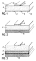
- This support includes a layer 2 of PMP and two metallic layers 4 and 6, made of the same metal. Layer 4 completely covers one face 8 of layer 2 while layer 6 partially covers the other face 10 of this layer 2.
- FIG. 2 differs from FIG. 1 by the fact that layer 4 is replaced there by a metal layer 16 made of a metal different from the metal which constitutes layer 6: the latter is for example made of copper and the layer 16 made of aluminum .
- a multilayer support a plurality of monolayer supports are produced (a single layer of PMP), as explained above, etching, if necessary, some of the corresponding metal layers by conventional techniques of manufacturing of printed circuits, these supports, called “elementary supports”, are superimposed, interposing between them layers of PMP called “intermediate layers” and the layers are pressed together using hot pressing .
- this pressing should be carried out at a temperature below the melting temperature of the elementary supports.
- a PMP of different grade is used for the intermediate layers than that which constitutes the elementary supports, and more precisely a PMP of which the softening temperature is lower than that of the PMP of elementary supports, but which has the same electrical properties.
- TPX the PMP marketed by the MITSUI Company, under the name TPX
- the elementary supports are made of TPX grade RT 18 (Vicat point 173 ° C) and pressed at 240 ° C
- intermediate layers are made of TPX grade MX 002 (Vicat point 145 ° C) and all of the layers are pressed at 235 ° C.
- the pressing of a multilayer support is carried out with the same pressure and cooling conditions as for elementary supports. Only the pressing tool must be adapted to take into account the thickness of the final support, or laminate, and the centering of the layers.
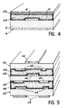
- FIGS. 3 to 5 schematically represent supports comprising several layers of PMP.
- an elementary support of the kind of that of FIG. 1 is produced, which comprises the metallic layers 4 and 6, and another metallic layer 18 is fixed on the layer 4 by means of an intermediate layer 20 of PMP.
- the metal layer 18 can be fixed to the metal layer 4 by means of any other adhesive. appropriate.
- an elementary support of the same type as that of FIG. 1 is still used and another metallic layer 22 is fixed on the face 10 of the layer 2, which carries the etched layer 6, by intermediate of an intermediate layer 24 of PMP.
- the support 26 carries, on one side, two etched metal layers 32 and, on the other side, two other etched metal layers 34.
- the support 28 carries, on one side, two etched metal layers 36 and, on the other side, another etched metal layer 38.
- the support 30 carries, on one side, two etched metal layers 42 and, on the other side, an etched metal layer 40.
- the elementary supports 26, 28 and 30 are fixed to each other by means of two intermediate layers 44 and 46 of PMP.
- the layers 34, 36, 38 and 42 are internal metallic layers while the layers 32 and 40 are external metallic layers.
- each of the layers 24 (FIG. 4), 44 and 46 (FIG. 5) can have not only an adhesive function but also a dielectric function and then have a thickness greater than 100 micrometers, which can range from a few hundreds of micrometers to several tens of mm.
- the characteristics of the PMP be modified, to adapt its mechanical and / or electrical characteristics for a given application. This must be done in such a way that the techniques for making supports which have been previously explained are retained. This can be achieved by adding various fillers, including mineral fillers, to the PMP.
- Metallic supports were produced in accordance with the present invention and these supports were subjected to standardized climato-mechanical tests and underwent these tests without degradation, inter alia the so-called “rapid temperature variation -65 ° C + 165 ° test C "and the test known as” climatic combination -30 ° C + 125 ° C, 90% relative humidity at 55 ° C ".
Landscapes
- Engineering & Computer Science (AREA)
- Microelectronics & Electronic Packaging (AREA)
- Manufacturing & Machinery (AREA)
- Physics & Mathematics (AREA)
- Plasma & Fusion (AREA)
- Thermal Sciences (AREA)
- Chemical & Material Sciences (AREA)
- Chemical Kinetics & Catalysis (AREA)
- Laminated Bodies (AREA)
Applications Claiming Priority (2)
| Application Number | Priority Date | Filing Date | Title |
|---|---|---|---|
| FR8911888 | 1989-09-12 | ||
| FR8911888A FR2651953B1 (fr) | 1989-09-12 | 1989-09-12 | Support metallise a base de polymethylpentene et procede de fabrication de ce support. |
Publications (2)
| Publication Number | Publication Date |
|---|---|
| EP0418148A1 true EP0418148A1 (de) | 1991-03-20 |
| EP0418148B1 EP0418148B1 (de) | 1995-12-27 |
Family
ID=9385348
Family Applications (1)
| Application Number | Title | Priority Date | Filing Date |
|---|---|---|---|
| EP90402502A Expired - Lifetime EP0418148B1 (de) | 1989-09-12 | 1990-09-11 | Verfahren zur Herstellung eines metallisierten Trägers auf Basis von Polymethylpenten |
Country Status (3)
| Country | Link |
|---|---|
| EP (1) | EP0418148B1 (de) |
| DE (1) | DE69024436T2 (de) |
| FR (1) | FR2651953B1 (de) |
Cited By (2)
| Publication number | Priority date | Publication date | Assignee | Title |
|---|---|---|---|---|
| FR2713139A1 (fr) * | 1993-12-03 | 1995-06-09 | Demeure Loic | Support métallisé à base de mousse organique, assemblage d'au moins deux de ces supports et procédé de fabrication de ce support. |
| EP2394814A1 (de) * | 2001-08-28 | 2011-12-14 | Avery Dennison Corporation | Kartenbogenkonstruktion |
Families Citing this family (1)
| Publication number | Priority date | Publication date | Assignee | Title |
|---|---|---|---|---|
| JP4029759B2 (ja) * | 2003-04-04 | 2008-01-09 | 株式会社デンソー | 多層回路基板およびその製造方法 |
Citations (4)
| Publication number | Priority date | Publication date | Assignee | Title |
|---|---|---|---|---|
| GB1186218A (en) * | 1966-06-08 | 1970-04-02 | Dynamit Nobel Ag | Improvements in or relating to Printed Circuits. |
| EP0149394A2 (de) * | 1983-12-29 | 1985-07-24 | Loic Demeure | Verfahren zur Herstellung eines aus Polypropylen bestehenden, mehrere metallische Schichten enthaltenden Trägers und durch dieses Verfahren erhaltener Träger |
| EP0262931A2 (de) * | 1986-09-30 | 1988-04-06 | Mitsubishi Kasei Corporation | Planare Antenne |
| EP0309143A2 (de) * | 1987-09-24 | 1989-03-29 | Mitsui Petrochemical Industries, Ltd. | Schichtstoffplatte für Hochfrequenz und Verfahren zu ihrer Herstellung |
-
1989
- 1989-09-12 FR FR8911888A patent/FR2651953B1/fr not_active Expired - Lifetime
-
1990
- 1990-09-11 DE DE69024436T patent/DE69024436T2/de not_active Expired - Fee Related
- 1990-09-11 EP EP90402502A patent/EP0418148B1/de not_active Expired - Lifetime
Patent Citations (4)
| Publication number | Priority date | Publication date | Assignee | Title |
|---|---|---|---|---|
| GB1186218A (en) * | 1966-06-08 | 1970-04-02 | Dynamit Nobel Ag | Improvements in or relating to Printed Circuits. |
| EP0149394A2 (de) * | 1983-12-29 | 1985-07-24 | Loic Demeure | Verfahren zur Herstellung eines aus Polypropylen bestehenden, mehrere metallische Schichten enthaltenden Trägers und durch dieses Verfahren erhaltener Träger |
| EP0262931A2 (de) * | 1986-09-30 | 1988-04-06 | Mitsubishi Kasei Corporation | Planare Antenne |
| EP0309143A2 (de) * | 1987-09-24 | 1989-03-29 | Mitsui Petrochemical Industries, Ltd. | Schichtstoffplatte für Hochfrequenz und Verfahren zu ihrer Herstellung |
Non-Patent Citations (1)
| Title |
|---|
| DATABASE DERWENT WPI, résumé no. 89-337619, Derwent Publications Ltd, Londres, GB; & JP-A-1 253 436 (SUMITOMO CHEM. IND. K.K.) 09-10-1989 * |
Cited By (2)
| Publication number | Priority date | Publication date | Assignee | Title |
|---|---|---|---|---|
| FR2713139A1 (fr) * | 1993-12-03 | 1995-06-09 | Demeure Loic | Support métallisé à base de mousse organique, assemblage d'au moins deux de ces supports et procédé de fabrication de ce support. |
| EP2394814A1 (de) * | 2001-08-28 | 2011-12-14 | Avery Dennison Corporation | Kartenbogenkonstruktion |
Also Published As
| Publication number | Publication date |
|---|---|
| FR2651953B1 (fr) | 1993-09-10 |
| FR2651953A1 (fr) | 1991-03-15 |
| DE69024436T2 (de) | 1996-07-25 |
| DE69024436D1 (de) | 1996-02-08 |
| EP0418148B1 (de) | 1995-12-27 |
Similar Documents
| Publication | Publication Date | Title |
|---|---|---|
| FR2527036A1 (fr) | Procede pour connecter un semiconducteur a des elements d'un support, notamment d'une carte portative | |
| WO1999046728A1 (fr) | Procede de fabrication de cartes sans contact | |
| CA2712381C (fr) | Procede de fabrication d'un element chauffant par depot de couches minces sur un substrat isolant, et l'element obtenu | |
| US5110387A (en) | Method for laminating polymer films | |
| FR2766618A1 (fr) | Procede de fabrication d'un film conducteur anisotrope a inserts conducteurs | |
| EP0418148B1 (de) | Verfahren zur Herstellung eines metallisierten Trägers auf Basis von Polymethylpenten | |
| WO2006037915A1 (fr) | Composant muni d'un ensemble de micropointes conductrices dures et procede de connexion electrique entre ce composant et un composant muni de protuberances conductrices ductiles | |
| EP0395544B1 (de) | Isolierte metallische Substrate und Verfahren zur Herstellung dieser Substrate | |
| EP0305267B1 (de) | Herstellungsverfahren der Gesamtheit von elektrisch leitenden Mustern auf einer Fläche aus isolierendem Material von komplexer Form | |
| CA1294861C (fr) | Procede de realisation d'un support a base de polypropylene comportant plusieurs couches metalliques et support obtenu par ce procede | |
| FR2674988A1 (fr) | Procede de fabrication d'un support de film a connexions electriques d'excellente solidite. | |
| EP0651458B1 (de) | Verfahren zur Herstellung einer ebenen Antenne | |
| EP0059206B1 (de) | Gedruckte schaltungsplatte und verfahren zu deren herstellung | |
| FR2713139A1 (fr) | Support métallisé à base de mousse organique, assemblage d'au moins deux de ces supports et procédé de fabrication de ce support. | |
| EP0140746B1 (de) | Verfahren zur Hitzebehandlung von elektrischleitenden Beschichtungen auf dielektrischen Trägern mittels Mikrowellen | |
| JPH05214511A (ja) | プラスチック部品の表面の金属被覆方法及び当該方法による部品 | |
| KR100461465B1 (ko) | Cu판을 포함하는 다층의 클래드 판재 제조 방법 | |
| FR2541826A1 (fr) | Procede de fabrication d'une cavite hyperfrequence et cavite obtenue par ce procede | |
| EP0056668A1 (de) | Verfahren zur Herstellung von Schichten von gedruckten Schaltungen und benutzbares Gerät | |
| CH620545A5 (en) | Method of manufacturing electrical resistors from a metal foil or film, application to obtaining thermoelectrical probes or strain gauges | |
| CN113905520A (zh) | 一种高结合力精细线路的制作方法及系统 | |
| CN119300232A (zh) | 一种可解决无机基板与金属线路结合力差问题的结构及其制作方法 | |
| WO2003019640A2 (fr) | Procede de mise en forme d'une couche mince et de formation d'une prise de contact | |
| WO2001030929A1 (fr) | Procede et moyens pour l'amelioration du collage entre materiaux polymeres, notamment pour carte a puce | |
| FR2524705A1 (fr) | Procede composite de fabrication de circuit hybride et circuit hybride obtenu par un tel procede |
Legal Events
| Date | Code | Title | Description |
|---|---|---|---|
| PUAI | Public reference made under article 153(3) epc to a published international application that has entered the european phase |
Free format text: ORIGINAL CODE: 0009012 |
|
| AK | Designated contracting states |
Kind code of ref document: A1 Designated state(s): DE GB |
|
| 17P | Request for examination filed |
Effective date: 19910822 |
|
| 17Q | First examination report despatched |
Effective date: 19930503 |
|
| RAP1 | Party data changed (applicant data changed or rights of an application transferred) |
Owner name: FRANCE TELECOM |
|
| GRAA | (expected) grant |
Free format text: ORIGINAL CODE: 0009210 |
|
| AK | Designated contracting states |
Kind code of ref document: B1 Designated state(s): DE GB |
|
| REF | Corresponds to: |
Ref document number: 69024436 Country of ref document: DE Date of ref document: 19960208 |
|
| GBT | Gb: translation of ep patent filed (gb section 77(6)(a)/1977) |
Effective date: 19960305 |
|
| PLBE | No opposition filed within time limit |
Free format text: ORIGINAL CODE: 0009261 |
|
| STAA | Information on the status of an ep patent application or granted ep patent |
Free format text: STATUS: NO OPPOSITION FILED WITHIN TIME LIMIT |
|
| 26N | No opposition filed | ||
| REG | Reference to a national code |
Ref country code: GB Ref legal event code: IF02 |
|
| PGFP | Annual fee paid to national office [announced via postgrant information from national office to epo] |
Ref country code: GB Payment date: 20080827 Year of fee payment: 19 |
|
| PGFP | Annual fee paid to national office [announced via postgrant information from national office to epo] |
Ref country code: DE Payment date: 20081002 Year of fee payment: 19 |
|
| GBPC | Gb: european patent ceased through non-payment of renewal fee |
Effective date: 20090911 |
|
| PG25 | Lapsed in a contracting state [announced via postgrant information from national office to epo] |
Ref country code: DE Free format text: LAPSE BECAUSE OF NON-PAYMENT OF DUE FEES Effective date: 20100401 |
|
| PG25 | Lapsed in a contracting state [announced via postgrant information from national office to epo] |
Ref country code: GB Free format text: LAPSE BECAUSE OF NON-PAYMENT OF DUE FEES Effective date: 20090911 |