EP0418492A2 - Schaltnetzteil - Google Patents
Schaltnetzteil Download PDFInfo
- Publication number
- EP0418492A2 EP0418492A2 EP90113784A EP90113784A EP0418492A2 EP 0418492 A2 EP0418492 A2 EP 0418492A2 EP 90113784 A EP90113784 A EP 90113784A EP 90113784 A EP90113784 A EP 90113784A EP 0418492 A2 EP0418492 A2 EP 0418492A2
- Authority
- EP
- European Patent Office
- Prior art keywords
- power supply
- magnetic path
- winding
- voltage
- control
- Prior art date
- Legal status (The legal status is an assumption and is not a legal conclusion. Google has not performed a legal analysis and makes no representation as to the accuracy of the status listed.)
- Withdrawn
Links
Images









Classifications
-
- H—ELECTRICITY
- H02—GENERATION; CONVERSION OR DISTRIBUTION OF ELECTRIC POWER
- H02M—APPARATUS FOR CONVERSION BETWEEN AC AND AC, BETWEEN AC AND DC, OR BETWEEN DC AND DC, AND FOR USE WITH MAINS OR SIMILAR POWER SUPPLY SYSTEMS; CONVERSION OF DC OR AC INPUT POWER INTO SURGE OUTPUT POWER; CONTROL OR REGULATION THEREOF
- H02M3/00—Conversion of DC power input into DC power output
- H02M3/22—Conversion of DC power input into DC power output with intermediate conversion into AC
- H02M3/24—Conversion of DC power input into DC power output with intermediate conversion into AC by static converters
- H02M3/28—Conversion of DC power input into DC power output with intermediate conversion into AC by static converters using discharge tubes with control electrode or semiconductor devices with control electrode to produce the intermediate AC
- H02M3/325—Conversion of DC power input into DC power output with intermediate conversion into AC by static converters using discharge tubes with control electrode or semiconductor devices with control electrode to produce the intermediate AC using devices of a triode or a transistor type requiring continuous application of a control signal
- H02M3/335—Conversion of DC power input into DC power output with intermediate conversion into AC by static converters using discharge tubes with control electrode or semiconductor devices with control electrode to produce the intermediate AC using devices of a triode or a transistor type requiring continuous application of a control signal using semiconductor devices only
- H02M3/337—Conversion of DC power input into DC power output with intermediate conversion into AC by static converters using discharge tubes with control electrode or semiconductor devices with control electrode to produce the intermediate AC using devices of a triode or a transistor type requiring continuous application of a control signal using semiconductor devices only in push-pull configuration
- H02M3/3376—Conversion of DC power input into DC power output with intermediate conversion into AC by static converters using discharge tubes with control electrode or semiconductor devices with control electrode to produce the intermediate AC using devices of a triode or a transistor type requiring continuous application of a control signal using semiconductor devices only in push-pull configuration with automatic control of output voltage or current
Definitions
- the present invention is directed to an improvement of control characteristics of a switching power supply for controlling an output voltage to a constant value with respect to fluctuations in input or in load.
- a switching power supply serves to supply a constant DC voltage with respect to a variety of loads by inputting a DC voltage which fluctuates.
- a voltage resonant type switching power supply is based on a system for switching by converting variations in voltages of semiconductor switches such as MOSFETs into sine waveforms which smoothly vary while utilizing an LC resonance.
- This type of switching power supply exhibits a characteristic of having a smaller switching loss and less noises caused during a switching operation than in prior art switching systems.
- FIG. 1 is a circuit diagram showing one example of the prior art switching power supply.
- the symbol Vi represents an input voltage
- 3 and 4 semiconductor switches such as MOSFETs connected in series to both ends of the input voltage Vi
- 5 and 6 excitation power sources connected between gate/source terminals of the MOSFETs 3 and 4, for driving the MOSFETs 3 and 4
- 11 a voltage resonant inductor one end of which is connected to a connecting point between the dividing capacitors 1 and 2
- 12 a transformer having a primary winding both ends of which are connected to a connecting point between the MOSFETs 3 and 4 as well as to the other end of the voltage resonant inductor 11
- 13 and 14 rectifying diodes having anodes
- Designated at 18 and 19 are a filter capacitor and a load resistor which are connected between the other end of the choke coil 17 and a mid-point of the secondary winding of the transformer 12.
- the choke coil 17 and the filter capacitor 18 are combined to constitute an output filter.
- the symbol Vo denotes an output voltage impressed on both ends of the load resistor 19.
- Indicated at Vh is an output voltage of a Half-bridge circuit constructed of components ranging from the dividing capacitors 1 and 2 to the voltage resonant capacitors 9 and 10.
- the numeral 20 represents an output feedback circuit, consisting of dividing resistors 21 and 22, a reference voltage 23, a comparator 24 and an ON time control circuit 25, for changing an ON time of switching of the MOSFETs 3 and 4, corresponding to a difference between the output voltage Vo and a reference voltage.
- FIG. 2 is an operating waveform diagram of assistance in explaining an operation of the device depicted in FIG. 1.
- FIG. 2(1) indicates an output of the excitation power source 5, i.g., a gate drive signal of a MOSFET 3 which is turned ON at a high level thereof;
- FIG. 2(2) an output of the excitation power source 6, viz., a gate drive signal of a MOSFET 4 which is turned ON at a high level thereof;
- FIG. 2(3) a drain-source voltage of the MOSFET 3;
- FIG. 2(4) a drain current of the MOSFET 3;
- FIG. 2(5) a drain current of the MOSFET 4;
- FIG. 2(6) a current flowing in the primary winding of the transformer 12 and the voltage resonant inductor 11;
- FIG. 2(7) a current flowing in the dividing capacitors 1 and 2; and
- FIG. 2(8) a current flowing in the voltage resonant capacitors 9 and 10.
- the MOSFETs 3 and 4 are turned ON alternately for a given period of time by the excitation power sources 5 and 6.
- the MOSFET 3 is turned ON at a timing t0, the current depicted in FIG. 2(4) flows in the MOSFET 3.
- a negative current flows in the parasitic diode 7 and works to regenerate the energy to an input.
- a resonant state is developed during a period ranging from t1 to t2 by use of the voltage resonant capacitors 9 and 10 in combination with the voltage resonant inductor 11.
- a voltage at both ends of the voltage resonant capacitor 10 is, though a period from t2 to t3 originally assumes the resonant state, held at substantially zero for the parasitic diode 8.
- an input voltage Vi is applied to both ends of the MOSFET 3, while both ends of the MOSFET 4 assume substantially zero voltage.
- the MOSFET 4 is turned ON (timing t3), and a switching loss is thereby remarkably reduced (zero voltage switching ).
- the MOSFET 4 is kept ON during a period from t3 to t4.
- the ON time of the MOSFETs 3 and 4 is changed by use of the ON-time control circuit 25 in accordance with an output error detected by the dividing resistors 21 and 22 in combination with the reference voltage 23 and the comparator 24. That is, if the output voltage is small, the ON time is increased (both a switching cycle and a duty become large), and much input power is conveyed to the output side. Whereas if large, the ON time is decreased. Note that an OFF time is determined by a resonant frequency and is therefore invariable. As a result, the switching frequency has to be changed for the output control.
- the secondary side can be replaced by a current source lo.
- the Half-bridge circuit consisting of the components ranging from the dividing capacitors 1 and 2 to the voltage resonant capacitors 9 and 10
- its circuitry can be expressed in a simplified circuit block diagram where the circuit is, as shown in FIG. 3, composed of the input voltage Vi, the DC-AC converter 26, the voltage resonant inductor 11, the load resistor 19 and the current source lo.
- the arrangement that the load resistor 19 and the voltage resonant inductor 11 are connected in series causes an increment in output impedance, whereby the output voltage Vo undergoes a great influence exerted by the fluctuations in load.
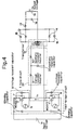
- FIG. 4 there is shown a circuit block diagram of a first embodiment of a switching power supply according to the present invention.
- a difference in arrangement between FIG. 4 and FIG. 1 lies in provision of a T type circuit 30 composed of two pieces of resonant inductors (one is referred to as a voltage resonant inductor 31, and the other is an auxiliary resonant inductor 32) which are employed in place of the voltage resonant inductor 11 and connected in series between a connecting point of MOSFETs 3 and 4 and one end of a primary winding of a transformer 12, and an auxiliary resonant capacitor 33 having one end connected a connecting point of the two resonant inductors 31 and 32 and the other end connected to a connecting point of the other end of the primary winding of the transformer 12 to a connecting point of dividing capacitors 1 and 2.
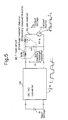
- the circuitry thereof can be expressed in a simplified circuit block diagram where the circuit is, as illustrated in FIG. 5, constructed of an input voltage Vi, a DC-AC converter 26, a T type circuit 30, a load resistor 19 and the current source lo.
- a voltage Vh between a connecting point of the dividing capacitors 1 and 2 and a connecting point of semiconductor switches 3 and 4-i. e., an output voltage of the DC-AC converter 26- is expressed by such a trapezoidal waveform that a peak value is given by (input voltage Vi)/2 as shown in FIG. 5.
- a current i1 flowing in an auxiliary resonant inductor 32 is expressed by a trapezoidal waveform where the peak value is a load current lo as indicated in FIG. 5.
- Lr is the inductance of a voltage resonant inducttor 31
- Ls is the inductance of an auxiliary resonant inductor 32
- Cs is the capacitance of an auxiliary resonant capacitor 33
- i2 is the current flowing in the auxiliary resonant capacitor 33.
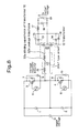
- FIG. 6 is a circuit block diagram illustrating a second embodiment of the voltage resonant type switching power supply of the invention.
- the T type circuit 30 consisting of the voltage resonant inductor 31, the auxiliary resonant inductor 32 and the auxiliary resonant capacitor 33 is provided on the side of the secondary winding of the transformer 12.
- the numerals 34-37 shown in the Figure represent rectifying diodes.
- the operation of this embodiment is the same as that of the device depicted in FIG. 4, and the description is therefore omitted herein.
- the condition (a constant of the T type circuit 30) for eliminating the fluctuations in load in this embodiment is that the inductance Lr of the voltage resonant inductor 31 be substitutively expressed such as Lr/N 2 where N is the turn ratio of the transformer 12, the inductance Ls of the auxiliary resonant inductor 32 be likewise expressed by Ls/N 2 , and the capacitance Cs of the auxiliary resonant capacitor 33 be likewise given by N 2 Cs.
- a conditional formula to eliminate the influence by the fluctuations in load is identical with the formulae (4) and (5), wherein the influence by the fluctuations in load on the output voltage disappears. Only the dependency associated with the fluctuations in input still exists, and hence a control range of the output voltage can be narrowed.
- FIG. 7(1) is a circuit block diagram showing a third embodiment of the switching power supply classified as a voltage resonant type according to the present invention.
- a difference between FIG. 7(1) and FIG. 4 is the arrangement that a leakage inductance 32a on the primary side of the transformer 12 is employed as a substitute for the auxiliary resonant inductor 32, connected to one end of the primary winding of ihe transformer 12, of the two resonant inductors constituting the T type circuit.
- the output voltage Vo is determined only by the input voltage Vi, whereby the output voltage is not, as in the case of the device depicted in FIG. 4, subjected to the influence by the fluctuations in load.
- the T type circuit is constructed by utilizing the leakage inductance of the transformer, unlike the device of FIG. 4 one of the two resonant inductors becomes unnecessary, resulting in a reduction in the number of components and an improvement of the reliability as well.
- the leakage inductance 32a on the primary side or, as illustrated in FIG. 7(2), leakage inductances 32a1 and 32a2 on the secondary side because of their being equivalent.
- the leakage inductance Le of the conditional formulae to remove the influence by the fluctuations in load which is shown in formulae (7) and (8) may be arranged to be a primary-side conversion value.
- a leakage inductance of the transformer 12 may be used as a substitute for the voltage resonant inductor 31 connected to one end of the secondary winding of the transformer 12, and the same effects as those of the device shown in FIG. 7 can also be obtained.
- FIG. 8 is a circuit block diagram showing a fourth embodiment of the switching power supply of the invention.
- a difference in arrangement between FIGS. 8 and 7(1) is that a winding capacitance 33a of the primary winding of the transformer 12 substitutes for the auxiliary resonant capacitor 33 constituting the T type circuit.
- the operation of the fourth embodiment is identical with that of the device shown in FIG. 4, and the explanation is therefore elided herein.
- a condition to disappear the influence by the fluctuations in load in the conditional equation shown in the formulae (7) and (8) is expressed by replacing the capacitance Cs of the auxiliary resonant capacitor 33 with the winding capacitance Cw of the primary winding of the transformer 12.
- the I type circuit is constructed by utilizing the winding capacitance of the transformer, the necessity for the auxiliary resonant capacitor is removed unlike the device of FIG. 7, the number of components can be reduced as well ameliorating the reliability.
- the leakage inductance of the transformer 12 may be employed as a substitute for the voltage resonant inductor 31.
- the winding capacitance of the secondary winding of the transformer 12 may also be used in place of the auxiliary resonant capacitor 33.
- FIG. 9 is a circuit block diagram illustrating a fifth embodiment of the switching power supply of the invention.
- the voltage resonant capacitors 9 and 10 are connected to both ends of the MOSFETs 3 and 4.
- the current as illustrated in FIG. 2(7) , constantly flows in the dividing capacitors 1 and 2 for dividing the input voltage Vi, thereby augmenting the effective current flowing in the dividing capacitors 1 and 2.
- large-sized capacitors each having an allowable ripple current have to be used as the dividing capacitors 1 and 2 to restrain the emission of heat. This is a factor of hindering the miniaturization of the device, which is emphasized in the fifth embodiment of the present invention.
- the device can be miniaturized by reducing the RMS current of the dividing capacitors for dividing output voltage.
- FIG. 4 the voltage resonant capacitors are connected to both ends of the MOSFETs 3 and 4.
- a voltage resonant capacitor 27 is connected to between a connecting point of the dividing capacitors 1 and 2 and a connecting point of the MOSFETs 3 and 4.
- FIG. 10 there is illustrated an operating mode diagram of assistance in explaining a state where the current on the primary side is generated by splitting into four operating modes a period from t1 to t5 shown in the operational waveform diagram of FIG. 2.
- both of the MOSFETs 3 and 4 are turned OFF during a period from t1 to t2 of FIG.
- the resonant state is present by virtue of a closed loop formed of the voltage resonant capacitor 27 and the T type circuit 30.
- no current flows in the dividing capacitors 1 and 2.
- the parasitic diode 8 is turned ON, while the voltage at both end of the voltage resonant capacitor 27 is kept at a constant level obtained by dividing the input voltage Vi with the dividing capacitors 1 and 2.
- the current flowing through the T type circuit 30 transits to currents Id1 and Id2 of the dividing capacitors 1 and 2.
- the MOSFET 4 is turned ON, and contrary to the period of FIG.
- the RMS value of the current flowing in the dividing capacitors 1 and 2 is reduced by a quantity equivalent to the portion of the oblique lines of FIG. 2(7), thereby decreasing an amount of the heat evolved from the dividing capacitors 1 and 2.
- a small-sized capacitor having a small allowable ripple current can be employed, resulting in the miniaturization of the device.
- the fifth embodiment may be applied to the device arranged in such a manner that the T type circuit 30 illustrated in FIG. 6 is provided on the side of the secondary winding of the transformer and further to the device which utilizes the leakage inductances of FIGS. 7 and 8 and the winding capacitance of the transformer as well. Even in such a case, the same effects can be exhibited.
- FIG. 11 is a circuit block diagram depicting an embodiment where the present invention is applied to a current control type magnetic amplifier constant voltage power supply.
- a prior art current control type magnetic amplifier constant voltage power supply takes such a configuration that an inductor 42 and a capacitor 43 are removed from the components shown in FIG. 11.
- the numeral 44 denotes a rectifying diode.
- Designated at 41 is a current control type magnetic amplifier for controlling the output, which may be conceived as a kind of variable inductor capable of controlling the output by varying the inductance in accordance with the fluctuations in input or in load. Based on this construction, the arrangement thereof is similar to that of the voltage resonant switching power supply illustrated in PIG. 4.
- the power supply is not classified as a resonant type.
- the semiconductor switches 3 and 4 are alternately turned ON at a constant frequency, and an output waveform Vh of a Half-bridge circuit (26) takes, as illustrated in the figure, a pulse form.
- a possible arrangement of the current control type magnetic amplifier constant voltage power supply illustrated in FIG. 11 is that the leakage inductance of the transformer 12 may substitute for the inductor 42, and the capacitor 43 may involve the use of winding capacitance of the transformer 12.
- FIG. 12 there is shown a circuit block diagram of a sixth embodiment of the switching power supply classified as a voltage resonant type according to the present invention.
- the resonant element involves the use of a fixed inductor or a fixed capacitor in the conventional example depicted in FIG. 1 to keep the resonant frequency constant, and it is required that the switching frequency be varied to control the output voltage.
- the switching frequency does, however, fluctuate depending on the fluctuations in load or in input, and the output filter has to be designed while setting the frequency at the minimum. This leads to a difficulty of miniaturizing the device.
- the switching frequency varies over a wide range, and for this reason the noise filter has to cover the wide range. A large-sized filter is needed.
- An emphasis of the sixth embodiment of the invention is placed on this point, wherein the output voltage can be controlled while the switching frequency remains fixed.
- FIGS. 12 and 4 the different arrangement between FIGS. 12 and 4 will be given as follows.
- One of the two resonant inductors which constitute the T type circuit is used as a variable inductor 28 a control current Ic of which is increased or decreased by an output voltage control circuit 50 in accordance with a difference between the output voltage Vo and the reference voltage.
- An inductance of the variable inductor 28 is varied by the control current Ic to control the output voltage Vo to a constant value.
- the output voltage control circuit 50 comprises dividing resistors 51 and 52, a reference voltage 53, a comparator 54 for effecting amplification by taking a difference between the output voltage divided by the dividing resistors 51 and 52 and the reference voltage 53, a phase compensation circuit 55, whose power source is driven by the voltage at both end of the load resistor 19, for performing a phasic compensation on the output of the comparator 54, and a current controlling transistor 56 for effecting a current amplification on the output of the phase compensation circuit 55 and driving a control winding of the variable inductor 28.
- the voltage at both ends of the load resistor 19 is split by the dividing resistors 51 and 52.
- the comparator 54 functions to take a difference between the divided output voltage and the reference voltage 53 and, after making the amplification, effects out the phasic compensation on the output thereof. Thereafter, a current conversion is carried out by means of the current controlling transistor 56 to change the control current Ic of the variable inductor 28. If the output voltage Vo is relatively large, the output voltage control circuit 50 operates to reduce the control current Ic. Whereas if relatively small, the circuit 50 operates to increase the control current Ic.
- the inductance of the variable inductor 28 is thereby varied, and the output voltage Vo is thus controlled.
- the load-dependency of the output voltage is remarkably reduced, and the output voltage Vo is approximately expressed by the followinq formula: where Ls is the inductance of the auxiliary resonant inductor 32, and Lr is the inductance of the variable inductor 28.
- the output voltage can be controlled while keeping the switching freguency constant by changing the inductance Ls of the auxiliary resonant inductor 32 or the inductance Lr of the variable inductor 28.
- a resonant freguency varies with the changes in this inductance, whereby inclinations of 1 and 2 shown in FIG. 2(3) vary. The variations in these inclinations do not exert any influence on the output voltage Vo if a condition to effect zero voltage switching is satisfied.
- the leakage inductance of the transformer 12 may substitute for the auxiliary resonant inductor 32 constituting the T type circuit 30C in the device depicted in FIG. 12, and the auxiliary resonant capacitor 33 may involve the use of the winding capacitance of the. transformer 12.
- This arrangement contributes to a reduction in the number of components as compared with the device of FIG. 12 as well as improving the reliability.
- FIG. 13 is a circuit block diagram illustrating a variant embodiment of the device of FIG. 12.
- This variant embodiment does not entail the use of the T type circuit.
- the variable inductor 28 is employed instead of the voltage resonant inductor 11 shown in FIG. 1, and there is provided the output voltage control circuit 50 for increasing or decreasing the control current Ic of the variable inductor 28 according to a difference between the output voltage Vo and the reference voltage.
- the inductance of the variable inductor 28 is changed by the control current Ic to control the output voltage Vo to a constant value.
- the output voltage Vo is approximately expressed by the following formula: where N is the ratio of turns on the primary side to those on the secondary side of the transformer 12, R is the load resistance and L is the inductance of the variable inductor 28.
- the inductance L is set small, the output voltage Vo increases. Whereas if set large, the output voltage Vo decreases.
- the control range of the output voltage becomes slightly wider than in the device of FIG. 12 by changing the inductance L of the variable inductor 28, but it is feasible to control the output voltage Vo while keeping the switching frequency constant.
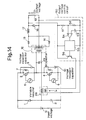
- FIG. 14 there is illustrated a circuit block diagram of a variant embodiment of the device depicted in FIG. 13.
- a capacitor 29 is connected to both ends of the primary winding of the transformer 12 instead of the snubber capacitors 15 and 16 of the device of FIG. 13.
- the output voltage Vo can, as in the way with the device of FIG. 13, be controlled while keeping the switching frequency constant, and at the same time the current flowing via the capacitor 29 does not run through the winding of the transformer. For this reason, designing the trs:" former 12 can be more facilitated than in the device depicted in FIG. 13.
- FIG. 15 is a circuit block diagram showing a seventh embodiment of the switching power supply conceived as a voltage resonant type according to the present invention.
- the difference in construction between FIGS. 15 and 12 is that there are provided two pieces of variable inductors constituting the T type circuit-one variable inductor 28a is formed with a feedforward loop from the input voltage, and the other variable inductor 28b is formed with a feedback loop from the output voltage.
- the T type circuit contributes a considerable shrinkage in the variation range of the variable inductor with respect to the fluctuations in load. In connection with the fluctuations in input, however, it is required that the variable inductor be changed substantially in proportion thereto. The variation range thereof is relatively large.
- the numeral 60 designates an input voltage control circuit for flowing, to the control winding of the variable inductor 28a, a control current Ic1 corresponding to variations in the input voltage Vi.
- the circuit 60 as illustrated in FIG. 16, works to perform a functional operation on an divided output voltage Ei obtained by dividing the input voltage Vi by use of dividing resistors R1 and R2.
- An output Eo thereof undergoes a current amplification by use of a circuit consisting of an OP-amp Op1, a transistor Q1 and a resistor Rf1, thus providing the control current Ic1 for driving the control winding of the variable inductor 28a.
- the control range of the variable inductor 28a becomes (A Lr1).
- the input fluctuations are slower than the load fluctuations in the switching power supply, and a quantity equivalent to the input fluctuations is controlled by the variable inductor 28a.
- the variable inductor 28b may therefore control a quantity equivalent to the load fluctuations, and a control range thereof becomes (A Lr2) shown in FIG. 17.
- variable inductor 28b a variation range of the variable inductor 28b is remarkably diminished, and the inductance of the control winding of the variable inductor 28b is thereby reduced. Consequently, the transient response can be improved. In addition, a small amount of control winding current may suffice, which in turn conducts to a reduction in control electric power needed for the output feedback.
- the control ranges (A Lr1 and A Lr2) are covered by the single variable inductor in the device of FIG. 12, and it follows that the number of turns of the control winding increases to deteriorate the response.
- the inductance of the variable inductor 28a augments, but the variable inductor 28a does not require a respondency as quick as the variable inductor 28b, which causes no problem.
- the number of turns of the control winding can be incremented, whereas the control power decreases. Consequently, total control electric power becomes smaller than in the conventional example.
- FIG. 19 is a circuit block diagram showing an eighth embodiment of the switching power supply classified as a voltage resonant type, of the present invention.
- the difference arrangement between FIGS. 19 and 12 lies in provision of a switch control circuit 70 for varying an ON time of switching of the MOSFETs 3 and 4 in accordance with the changes in input voltage.
- the switch control circuit 70 comprises dividing resistors 71 and 72 connected in series to both ends of the input voltage Vi, a functional operation circuit 73 for effecting a functional operation on the output voltages divided by the dividing resistors 71 and 72, and a gate driving control circuit 74 for controlling the ON time of switching of the MOSFETs 3 and 4 on the basis of an output of the functional operation circuit 73.
- a terminal IN of the gate driving control circuit 74 is employed during a parallel operation and serves to fetch a gate signal from the outside.
- signals transmitted from the dividing resistors 71 and 72 to the gate driving control circuit 74 are cut off, and input signals from the terminal IN are outputted intact from the gate driving control circuit 74.
- the input voltage Vi is split by the dividing resistors 71 and 72 of the switch control circuit 70, and the thus divided output voltages are, after undergoing an arithmetic operation by the functional operation circuit 73, converted into an ON time Ton of switching of the MOSFETs 3 and 4 by means of the gate driving control circuit 74.
- FIG. 20 there is shown a relationship between the ON time Ton of switching and the input voltage Vi, wherein the ON time Ton of switching becomes shorter as the input voltage Vi increases.
- An output waveform of the gate driving control circuit 74 is illustrated in FIG.
- a resonant condition of a T type circuit 30c in the device shown in FIG. 12 is typically designed by use of a representative value of an input specification.
- the inductance Lr of the variable inductor 28 greatly varies due to the control over the output voltage Vo, with the result that the auxiliary resonant condition (the formula (5)) is broken.
- the load dependency of the output voltage is not diminished. Therefore, the variation range of the inductance Lr of the variable inductor 28 due to the load fluctuations becomes considerably wider than in the establishment of the auxiliary resonant condition, and it follows that the quick respondency of the output voltage control to sharp variations in load is deteriorated.
- This embodiment emphatically deals with this point. As illustrated in FIG. 21, when changing the ON time Ton of switching, the switching frequency fs also changes.
- the current control type magnetic amplifier constant voltage power supply depicted in FIG. 11 may also be provided with the output voltage control circuit and the switch control circuit.
- the influence by the fluctuations in input voltage on the output voltage is lessened by controlling the ON time of the semiconductor switch according to the input voltage, and the variation width of inductance of the magnetic amplifier which is required for controlling the output voltage can also be narrowed.
- the switch control circuit is provided, and the ON time of the semiconductor switch is controlled corresponding to the input voltage, thereby reducing the influence by the fluctuations in input voltage on the output voltage. Besides, it is feasible to diminish the variation width of inductance of the variable inductor which is required for controlling the output voltage.
- the MOSFETs are, though not limited, employed as the semiconductor switches 3 and 4. Arbitrary electronic switch elements are also usable.
- variable inductors employed in the sixth to eight embodiments of the switching power supply of the present invention will be explained.
- FIG. 22 is a block diagram showing one embodiment of a prior art variable inductor.
- a winding a1-a2 serves as a control winding
- a winding b1-b2 serves as an inductor winding.
- Magnetic fluxes generated by a current flowing through the inductor winding b1-b2 wound separately on two magnetic path members act in opposite directions with respect to the magnetic path member along which the control winding a1-a2 is wound and are thereby offset each other, resulting in no generation of a voltage in the control winding a1-a2. It is therefore possible to reduce interferences of the control winding a1-a2 and of the inductor winding b1-b2.
- FIG. 23 is a block diagram illustrating a first embodiment of the variable inductor employed for the switching power supply of the invention.
- magnetic path members 16-18 are combined to shape a first magnetic path closed in a rectangular shape.
- the winding a1-a2 is a control winding wound along the magnetic path member 18.
- Magnetic path members 11-15 are combined to form an E-shaped second magnetic path. Ends of the three magnetic path members (11-13) assuming the E-like configuration are connected via air gaps g11-g13 to the magnetic path members 16-17 constituting the first magnetic path, as a result of which the magnetic path member 12 is used in common; and a pair of symmetric closed magnetic paths are formed on both sides thereof.
- the winding b1-b2 used as an inductor winding is wound along the magnetic path member 12.
- the closed magnetic path formed of the magnetic path members 16-18 is, when viewed from the control winding a1-a2, formed with no air gap, and the saturation can be effected by a small amount of current.
- a passage through the air gaps g11-g13 is invariably made in the case of providing a closed magnetic path formed of the magnetic path members 12 - 14 - 11 - 15 - 12 and a closed magnetic path formed of the magnetic path members 12 - 15 - 13 - 17 - 12. In consequence, a large current is needed for saturating the closed magnetic path composed of the magnetic path members 11-17.
- FIG. 24 is a block diagram illustrating a variant embodiment of the variable inductor of FIG. 23.
- the difference in arrangement between FIGS. 24 and 23 is that an air gap is formed only at the end of the magnetic path member 12 located in the middle of the E-shape.
- a proportion of the magnetic path members to be saturated increases, thereby making it possible to enlarge the variations in inductance.
- FIGS. 25 and 26 are equivalent circuit diagrams when being expressed by use of the magnetic resistances Ri and Rgi.
- the equivalent circuit diagram of FIG. 25 when viewed from the inductor winding b1-b2 If, this equation is established (if symmetric with respect to the magnetic path member 12), magnetic fluxes 0 1 and 0 2 generated by a magnetomotive force N111 are equalized, thereby causing no magnetic flux 0 3 passing through a magnetic resistance R8 between two points A and B. Namely, there is caused no interference with the control winding a1-a2 from the inductor winding b1-b2.
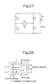
- FIG. 27 is an equivalent circuit diagram in which the equivalent circuit diagram of FIG. 26 is simplified for representation.
- the magnetic resistance when viewed from the control winding a1-a2 is expressed such as: If Z1 and Z3 contain the air gaps herein (corresponding to FIG. 23), generally the following relationship is given. and, The magnetic resistance R includes no resistance of the air gap and comes to have a small value, whereby larger magnetic flux can be produced by smaller control electric power. If Z1 and Z3 contain no air gap (corresponding to FIG. 24), the magnetic resistance R does not include the air gap and likewise comes to have a small value. On the other hand, the magnetic resistance Rg2 of the air gap is invariable included in the magnetic resistance when viewed from the inductor winding b1-b2. Therefore, the magnetic resistance R is increased by arbitrarily determining the air gap length dg2, and it is possible to prevent the core saturation even by the large magnetomotive force N111.
- FIG. 28 there is illustrated a block diagram of a second embodiment of the variable inductor used for the switching power source of the present invention.
- a pair of symmetric El- shaped closed magnetic paths are formed of the magnetic path members 12 - 14 - 11 - 16 - 12 and 12 - 15 - 13 - 17 - 12, which are provided in symmetry with respect to the magnetic path member 12.
- the winding a1-a2 may be defined as a control winding wound along the magnetic path member 12.
- a magnetic path member 18 assuming a substantially U-shape is connected via air gaps g14 and g15 to the magnetic path members 16 and 17, thus forming a closed magnetic path.
- the magnetic path member 18 is, as illustrated in the Figure, wound with the winding b1-b2 employed as an inductor winding, whereby, as in the case of the configuration of FIG. 23, the saturation can easily be performed from the control winding a1-a2 but is hard to be effected from the inductor winding b1-b2.
- a practicable arrangement is that the rectangularly-shaped first magnetic path may be connected to the E-shaped second magnetic path with no air gap.
- the control winding and the inductor winding may be wound along the magnetic path members on either side.
- FIG. 29 illustrates an embodiment in which a combination of two magnetic paths of the variable inductor depicted in FIG. 24 is changed.
- the configuration is such that a substantially U-shaped magnetic path shown in FIG. 29(1) is, as illustrated in FIG. 29(3), combined heightwise with an EI-shaped magnetic path shown in FIG. 29(2).
- This configuration is advantageous when a mounting area on, e. g., a printed board is limited. Besides, an area of the core wound with the control winding can be set large, whereby a larger radiation area of the core can be obtained.
- FIG. 29(4) is a bottom view of FIG. 29(3), wherein an air gap is formed only in the magnetic path member 12 of the EI-shaped magnetic path.
- the configuration is not, however, limited to this.
- the air gaps may be formed at the respective ends of the three magnetic path members 11 through 13 which cooperate to assume an E-like configuration; or alternatively the configuration may include no air gap.
- the switching power supply of the present invention exhibits the following advantages:
Landscapes
- Engineering & Computer Science (AREA)
- Power Engineering (AREA)
- Dc-Dc Converters (AREA)
Applications Claiming Priority (8)
| Application Number | Priority Date | Filing Date | Title |
|---|---|---|---|
| JP246915/89 | 1989-09-22 | ||
| JP24691589 | 1989-09-22 | ||
| JP337344/89 | 1989-12-26 | ||
| JP33734489 | 1989-12-26 | ||
| JP4741990 | 1990-02-28 | ||
| JP47419/90 | 1990-02-28 | ||
| JP107136/90 | 1990-04-23 | ||
| JP2107136A JP2720569B2 (ja) | 1989-06-19 | 1990-04-23 | スイッチング型定電圧電源 |
Publications (2)
| Publication Number | Publication Date |
|---|---|
| EP0418492A2 true EP0418492A2 (de) | 1991-03-27 |
| EP0418492A3 EP0418492A3 (en) | 1991-04-24 |
Family
ID=27462040
Family Applications (1)
| Application Number | Title | Priority Date | Filing Date |
|---|---|---|---|
| EP19900113784 Withdrawn EP0418492A3 (en) | 1989-09-22 | 1990-07-18 | Switching power supply |
Country Status (3)
| Country | Link |
|---|---|
| US (1) | US5065301A (de) |
| EP (1) | EP0418492A3 (de) |
| DE (1) | DE418492T1 (de) |
Cited By (4)
| Publication number | Priority date | Publication date | Assignee | Title |
|---|---|---|---|---|
| EP0963032A1 (de) * | 1998-05-30 | 1999-12-08 | Philips Patentverwaltung GmbH | AC-DC-Wandler |
| DE10144540A1 (de) * | 2001-09-11 | 2003-04-03 | Infineon Technologies Ag | Spannungswandler |
| WO2004027968A1 (en) * | 2002-09-20 | 2004-04-01 | Coutant Lambda Limited | Multi-resonant dc-dc converter |
| WO2007049220A3 (en) * | 2005-10-25 | 2008-03-13 | Koninkl Philips Electronics Nv | Power converter |
Families Citing this family (22)
| Publication number | Priority date | Publication date | Assignee | Title |
|---|---|---|---|---|
| MX9200368A (es) * | 1991-01-29 | 1992-08-01 | Dawari Datubo Dan Harry | Sistema de conversion de potencia de alta densidad y alta frecuencia. |
| US5291383A (en) * | 1992-09-02 | 1994-03-01 | Exide Electronics Corporation | Simplified UPS system |
| US5373432A (en) * | 1992-12-10 | 1994-12-13 | Hughes Aircraft Company | Fixed frequency DC to DC converter with a variable inductance controller |
| US5372045A (en) * | 1993-02-12 | 1994-12-13 | Rosemount Inc. | Bridge pulse controlled constant current driver for magnetic flowmeter |
| US5530638A (en) * | 1993-09-24 | 1996-06-25 | At&T Corp. | Multi-resonant electronic power converter with a wide dynamic range |
| JPH0819252A (ja) * | 1994-06-27 | 1996-01-19 | Nec Eng Ltd | 共振コンバータ |
| US5495404A (en) * | 1994-07-29 | 1996-02-27 | Motorola, Inc. | Multi-resonant inverter |
| US5723913A (en) * | 1994-12-06 | 1998-03-03 | Performance Controls, Inc. | High-voltage electronic switching circuit |
| JP2730506B2 (ja) * | 1995-02-27 | 1998-03-25 | 日本電気株式会社 | 圧電トランスを用いたdc/dcコンバータ |
| KR0177873B1 (ko) * | 1995-12-02 | 1999-05-15 | 변승봉 | 순환전류 프리형 고주파 소프트 스위칭FB(Full Bridge)DC-DC컨버터 |
| US5715155A (en) * | 1996-10-28 | 1998-02-03 | Norax Canada Inc. | Resonant switching power supply circuit |
| EP0930653B1 (de) * | 1998-01-13 | 2008-06-11 | Lucent Technologies Inc. | Hochfrequenzhalbleiteranordnung |
| US6181116B1 (en) | 1998-05-22 | 2001-01-30 | Nmb U.S.A. Inc. | Power regulator |
| US6151231A (en) * | 1998-12-31 | 2000-11-21 | Motorola, Inc. | Circuit and method for reactive energy recirculation control in a series-resonant converter |
| US6356461B1 (en) * | 2000-06-08 | 2002-03-12 | Mark E. Jacobs | Transformer flux observer for a full bridge power converter and method of operation thereof |
| US6483723B2 (en) * | 2000-11-07 | 2002-11-19 | Matsushita Electric Industrial Co., Ltd. | Switching power supply |
| DE10157836B4 (de) * | 2001-11-26 | 2004-02-19 | Infineon Technologies Ag | Signalverteilung zu einer Mehrzahl von Schaltungseinheiten |
| US7106605B2 (en) * | 2004-06-30 | 2006-09-12 | General Motors Corporation | DC converter circuit with overshoot protection |
| TW200742491A (en) * | 2006-04-17 | 2007-11-01 | Delta Electronics Inc | Power supply system for lighting lamp |
| US8619438B2 (en) * | 2011-05-19 | 2013-12-31 | Infineon Technologies Ag | Resonant converter |
| CN103105956B (zh) * | 2011-11-11 | 2015-05-06 | 汉王科技股份有限公司 | 位置指示装置及方法 |
| JP6617588B2 (ja) * | 2016-02-02 | 2019-12-11 | Tdk株式会社 | スイッチング電源装置 |
Family Cites Families (10)
| Publication number | Priority date | Publication date | Assignee | Title |
|---|---|---|---|---|
| US1227114A (en) * | 1915-07-15 | 1917-05-22 | American Telephone & Telegraph | Electrical receiving, translating, or repeating circuit. |
| IT1118548B (it) * | 1979-04-04 | 1986-03-03 | Wabco Westinghouse Spa | Convertitore statico autorisonante a regolazione estesa |
| US4409647A (en) * | 1981-03-12 | 1983-10-11 | Harry Terkanian | Power converter using a resonant circuit |
| US4415959A (en) * | 1981-03-20 | 1983-11-15 | Vicor Corporation | Forward converter switching at zero current |
| GB2170663B (en) * | 1985-02-02 | 1989-06-14 | Brian Ernest Attwood | Harmonic-resonant power supply |
| US4674019A (en) * | 1986-04-16 | 1987-06-16 | Keller-Mullett Technology | Transformer-coupled two-inductor buck converter |
| US4860184A (en) * | 1987-09-23 | 1989-08-22 | Virginia Tech Intellectual Properties, Inc. | Half-bridge zero-voltage switched multi-resonant converters |
| US4841220A (en) * | 1987-09-23 | 1989-06-20 | Tabisz Wojciech A | Dc-to-Dc converters using multi-resonant switches |
| US4814962A (en) * | 1988-05-27 | 1989-03-21 | American Telephone And Telegraph Company, At&T Bell Laboratories | Zero voltage switching half bridge resonant converter |
| US4991075A (en) * | 1989-02-14 | 1991-02-05 | Mitsubishi Denki Kabushiki Kaisha | Low-switching loss DC-DC converter |
-
1990
- 1990-07-05 US US07/548,010 patent/US5065301A/en not_active Expired - Fee Related
- 1990-07-18 EP EP19900113784 patent/EP0418492A3/en not_active Withdrawn
- 1990-07-18 DE DE199090113784T patent/DE418492T1/de active Pending
Cited By (5)
| Publication number | Priority date | Publication date | Assignee | Title |
|---|---|---|---|---|
| EP0963032A1 (de) * | 1998-05-30 | 1999-12-08 | Philips Patentverwaltung GmbH | AC-DC-Wandler |
| DE10144540A1 (de) * | 2001-09-11 | 2003-04-03 | Infineon Technologies Ag | Spannungswandler |
| EP1292005A3 (de) * | 2001-09-11 | 2004-08-25 | Infineon Technologies AG | Spannungswandler |
| WO2004027968A1 (en) * | 2002-09-20 | 2004-04-01 | Coutant Lambda Limited | Multi-resonant dc-dc converter |
| WO2007049220A3 (en) * | 2005-10-25 | 2008-03-13 | Koninkl Philips Electronics Nv | Power converter |
Also Published As
| Publication number | Publication date |
|---|---|
| US5065301A (en) | 1991-11-12 |
| DE418492T1 (de) | 1991-08-14 |
| EP0418492A3 (en) | 1991-04-24 |
Similar Documents
| Publication | Publication Date | Title |
|---|---|---|
| EP0418492A2 (de) | Schaltnetzteil | |
| US6061252A (en) | Switching power supply device | |
| US6807069B2 (en) | Direct current converter with integrated transformer windings and output voltage filtering coils on the same magnetic core | |
| KR100398565B1 (ko) | 플라이백변환기 | |
| US4777406A (en) | High voltage power supply particularly adapted for a TWT | |
| US6587358B1 (en) | Switching power supply circuit | |
| KR100733665B1 (ko) | Dc 컨버터 | |
| US20070024255A1 (en) | Switching power supply circuit | |
| US7053505B2 (en) | Amplifying circuit, noise reducing apparatus and power converting apparatus | |
| EP0602834A1 (de) | Spannungsteuerschaltungen | |
| US4829232A (en) | Nonlinear resonant switch and converter | |
| US6198644B1 (en) | Rectifying/smoothing circuit and double-ended converter | |
| US4292544A (en) | Power control circuit | |
| EP0227042A2 (de) | Hochspannungsquelle für kontinuierlich geregelte Ausgangsspannung, vorzugsweise um Ionen- und Elektronenstrahl-Bearbeitungs- und -Verdampfungsgeräte mit niedriger Leistung zu speisen | |
| US4371918A (en) | High efficiency push-pull saturation converter | |
| JP2003259644A (ja) | スイッチングコンバータ回路 | |
| JP2720569B2 (ja) | スイッチング型定電圧電源 | |
| JPH067746B2 (ja) | 電圧共振型スイッチング電源 | |
| US4215391A (en) | Power conversion device | |
| JPS61277372A (ja) | 電源装置 | |
| JPH0576178A (ja) | スイツチング電源装置 | |
| JPH08317633A (ja) | スイッチング電源用の平滑回路 | |
| JPH0739149A (ja) | 電圧共振コンバータ用整流平滑回路 | |
| JPH06112064A (ja) | 電力変換回路 | |
| JPH067745B2 (ja) | 電流共振型コンバータ |
Legal Events
| Date | Code | Title | Description |
|---|---|---|---|
| PUAI | Public reference made under article 153(3) epc to a published international application that has entered the european phase |
Free format text: ORIGINAL CODE: 0009012 |
|
| PUAL | Search report despatched |
Free format text: ORIGINAL CODE: 0009013 |
|
| 17P | Request for examination filed |
Effective date: 19900814 |
|
| AK | Designated contracting states |
Kind code of ref document: A2 Designated state(s): DE GB NL |
|
| AK | Designated contracting states |
Kind code of ref document: A3 Designated state(s): DE GB NL |
|
| TCNL | Nl: translation of patent claims filed | ||
| DET | De: translation of patent claims | ||
| 17Q | First examination report despatched |
Effective date: 19930420 |
|
| STAA | Information on the status of an ep patent application or granted ep patent |
Free format text: STATUS: THE APPLICATION IS DEEMED TO BE WITHDRAWN |
|
| 18D | Application deemed to be withdrawn |
Effective date: 19950224 |