EP0418802A2 - Structure de conducteurs dans un circuit intégré à échelle de plaquette - Google Patents
Structure de conducteurs dans un circuit intégré à échelle de plaquette Download PDFInfo
- Publication number
- EP0418802A2 EP0418802A2 EP90117908A EP90117908A EP0418802A2 EP 0418802 A2 EP0418802 A2 EP 0418802A2 EP 90117908 A EP90117908 A EP 90117908A EP 90117908 A EP90117908 A EP 90117908A EP 0418802 A2 EP0418802 A2 EP 0418802A2
- Authority
- EP
- European Patent Office
- Prior art keywords
- functional blocks
- wafer
- integrated circuit
- scale integrated
- semiconductor wafer
- Prior art date
- Legal status (The legal status is an assumption and is not a legal conclusion. Google has not performed a legal analysis and makes no representation as to the accuracy of the status listed.)
- Granted
Links
Images




Classifications
-
- H—ELECTRICITY
- H10—SEMICONDUCTOR DEVICES; ELECTRIC SOLID-STATE DEVICES NOT OTHERWISE PROVIDED FOR
- H10W—GENERIC PACKAGES, INTERCONNECTIONS, CONNECTORS OR OTHER CONSTRUCTIONAL DETAILS OF DEVICES COVERED BY CLASS H10
- H10W20/00—Interconnections in chips, wafers or substrates
- H10W20/40—Interconnections external to wafers or substrates, e.g. back-end-of-line [BEOL] metallisations or vias connecting to gate electrodes
- H10W20/41—Interconnections external to wafers or substrates, e.g. back-end-of-line [BEOL] metallisations or vias connecting to gate electrodes characterised by their conductive parts
- H10W20/427—Power or ground buses
-
- H—ELECTRICITY
- H10—SEMICONDUCTOR DEVICES; ELECTRIC SOLID-STATE DEVICES NOT OTHERWISE PROVIDED FOR
- H10W—GENERIC PACKAGES, INTERCONNECTIONS, CONNECTORS OR OTHER CONSTRUCTIONAL DETAILS OF DEVICES COVERED BY CLASS H10
- H10W72/00—Interconnections or connectors in packages
-
- H—ELECTRICITY
- H10—SEMICONDUCTOR DEVICES; ELECTRIC SOLID-STATE DEVICES NOT OTHERWISE PROVIDED FOR
- H10W—GENERIC PACKAGES, INTERCONNECTIONS, CONNECTORS OR OTHER CONSTRUCTIONAL DETAILS OF DEVICES COVERED BY CLASS H10
- H10W72/00—Interconnections or connectors in packages
- H10W72/50—Bond wires
-
- H—ELECTRICITY
- H10—SEMICONDUCTOR DEVICES; ELECTRIC SOLID-STATE DEVICES NOT OTHERWISE PROVIDED FOR
- H10W—GENERIC PACKAGES, INTERCONNECTIONS, CONNECTORS OR OTHER CONSTRUCTIONAL DETAILS OF DEVICES COVERED BY CLASS H10
- H10W72/00—Interconnections or connectors in packages
- H10W72/071—Connecting or disconnecting
- H10W72/075—Connecting or disconnecting of bond wires
- H10W72/07531—Techniques
- H10W72/07532—Compression bonding, e.g. thermocompression bonding
- H10W72/07533—Ultrasonic bonding, e.g. thermosonic bonding
-
- H—ELECTRICITY
- H10—SEMICONDUCTOR DEVICES; ELECTRIC SOLID-STATE DEVICES NOT OTHERWISE PROVIDED FOR
- H10W—GENERIC PACKAGES, INTERCONNECTIONS, CONNECTORS OR OTHER CONSTRUCTIONAL DETAILS OF DEVICES COVERED BY CLASS H10
- H10W72/00—Interconnections or connectors in packages
- H10W72/50—Bond wires
- H10W72/541—Dispositions of bond wires
- H10W72/5453—Dispositions of bond wires connecting between multiple bond pads on a chip, e.g. daisy chain
-
- H—ELECTRICITY
- H10—SEMICONDUCTOR DEVICES; ELECTRIC SOLID-STATE DEVICES NOT OTHERWISE PROVIDED FOR
- H10W—GENERIC PACKAGES, INTERCONNECTIONS, CONNECTORS OR OTHER CONSTRUCTIONAL DETAILS OF DEVICES COVERED BY CLASS H10
- H10W72/00—Interconnections or connectors in packages
- H10W72/50—Bond wires
- H10W72/551—Materials of bond wires
- H10W72/552—Materials of bond wires comprising metals or metalloids, e.g. silver
- H10W72/5522—Materials of bond wires comprising metals or metalloids, e.g. silver comprising gold [Au]
-
- H—ELECTRICITY
- H10—SEMICONDUCTOR DEVICES; ELECTRIC SOLID-STATE DEVICES NOT OTHERWISE PROVIDED FOR
- H10W—GENERIC PACKAGES, INTERCONNECTIONS, CONNECTORS OR OTHER CONSTRUCTIONAL DETAILS OF DEVICES COVERED BY CLASS H10
- H10W72/00—Interconnections or connectors in packages
- H10W72/50—Bond wires
- H10W72/551—Materials of bond wires
- H10W72/552—Materials of bond wires comprising metals or metalloids, e.g. silver
- H10W72/5524—Materials of bond wires comprising metals or metalloids, e.g. silver comprising aluminium [Al]
-
- H—ELECTRICITY
- H10—SEMICONDUCTOR DEVICES; ELECTRIC SOLID-STATE DEVICES NOT OTHERWISE PROVIDED FOR
- H10W—GENERIC PACKAGES, INTERCONNECTIONS, CONNECTORS OR OTHER CONSTRUCTIONAL DETAILS OF DEVICES COVERED BY CLASS H10
- H10W72/00—Interconnections or connectors in packages
- H10W72/90—Bond pads, in general
- H10W72/931—Shapes of bond pads
- H10W72/932—Plan-view shape, i.e. in top view
Definitions
- the present invention relates to a wiring structure in a semiconductor wafer-scale integrated circuit (hereinafter referred to as an IC).
- a wafer-scale IC comprises a plurality of identical functional blocks, having memories and logic circuits for control thereof, and operates as a single device without separating these blocks. Therefore, the wafer-scale IC can integrate circuitry on a larger scale than any other IC, and can reduce signal delay time due to the provision of shorter wiring distances between IC chips than is the case for a conventional plurality of ICs each being an individual IC chip in a package. Moreover, since processes for assembling individual IC chips are naturally unnecessary, circuit fabrication processes for wafer-scale ICs can be simplified, and accordingly device reliability can be improved. Recent wafer-scale ICs provide a memory capacity of 200 M bits on a single wafer 15 cm in diameter.
- Fig. 1 schematically shows a plan view of a wafer-scale IC.
- a wafer 11 having 26 rows x 9 columns of functional blocks 12 is mounted on a circuit board (not illustrated), formed of resin, etc., called a carrier.
- Fig. 2(a) is a plan view showing to an enlarged scale that part of Fig. 1 enclosed by broken lines.
- Functional blocks 12 are fabricated by repeated exposures of a reticule of a single block, for rows and columns in a matrix, in a step and repeat method. Therefore, terminal electrodes (pads) 14 for the supply of source voltages to the functional blocks are aligned in lines.
- lengths of power-supply layer-wiring 13 for supplying source voltage to each of the functional blocks are connected in series via pads, and each pad is connected in parallel to each functional block on a line, as shown in Fig. 2(a).
- Wiring 13 is connected to the carrier (not illustrated) by a bonding wiring via terminal electrodes (not illustrated) provided at an edge part of wafer 11, so as to receive power source voltage.
- Power supply layer-wiring 13 is usually formed by a metal film pattern about several tens of micrometres in width and about 1 ⁇ m in thickness. As this power supply layer-wiring extends from one edge to another edge of a wafer as large as 15 cm in diameter, its resistance and inductance are both increased.
- connection to adjacent functional blocks is effected by overlapping the patterned wiring at the connecting areas of the blocks during exposures for forming the functional blocks using the reticule.
- reticule exposure of such a large pattern cannot easily maintain alignment accuracy at peripheral parts thereof, and the wafer itself does not always have sufficient surface flatness since many layers have been already fabricated thereon prior to formation of the layer-wiring, resulting in a problem in terms of reliability in comparison with the layer wiring usually formed by a single patterning.
- power supply terminals 14 of each functional block may be connected by bonding wires 17 as shown in Fig. 2(b), in place of layer-wiring 13.
- bonding wire 17 is typically formed of aluminium or gold 30 to 100 ⁇ m in diameter, its resistance and inductance can be significantly lower than that of layer wiring 13. However, even if a bonding wire is employed, since the power source voltage is supplied via serially-connected wirings to as many as (typically) twenty-six functional blocks, a single wire-break results in failure of power supply to all the functional blocks beyond the broken wiring point, resulting in a reliability problem for the device.
- the above-explained structure, where the power supply wiring is constituted by layer wiring or is constituted by bonding wire is described in European Patent Application No. 89401508.5.
- An embodiment of the present invention can provide a wafer-scale integrated circuit, formed on a single wafer, wherein reliable wiring connections to each of the functional blocks fabricated therein is secured.
- pad electrodes for receiving a common voltage and provided on each of a plurality of identical functional blocks, are connected with each other dually by layered wirings as well as bonding wires.
- connection wirings connection failure modes are different for the respective wiring types, resulting in an increased reliability of the wafer-scale integrated circuit.
- dually connected wirings are advantageous particularly in the case where wirings between adjacent functional blocks are serially connected with each other so as to commonly supply the power source voltage via the connection electrodes provided thereon to the functional blocks.
- Fig. 3(a) is a schematic plan view illustrating a basic embodiment of the present invention.
- the numerals 12A, 12B, Vietnamese of Fig. 3 indicate a plurality of functional blocks fabricated on a single wafer of 15 cm diameter, as shown in Fig. 1.
- Each of the functional blocks is, for example, 13.65 x 4.4 mm in size, and comprises therein, for example, a 1 M bit DRAM (dynamic random access memory) and its control circuit.
- DRAM dynamic random access memory
- An example of details of each functional block and the overall structure of a wafer will be explained below.
- Each functional block is fabricated, as is well known, by a step and repeat method in which a reticule having the pattern of a single functional block is repeatedly exposed by selecting desired matrix positions upon semiconductor wafer 11. Therefore, connection terminals 14 provided for receiving power source voltages Vcc, Vss, etc., from circuits external to the functional blocks are aligned, on straight lines in the example illustrated.
- Layer wirings 13A, 13B, 13C, Vietnamese, used to supply power source voltage, such as Vcc or Vss, to each of the functional blocks are typically about 50 ⁇ m wide, about 1 ⁇ m thick and typically formed of aluminium film, and are sequentially connected to each of a series of power supply terminals 14A, 14B, 14C, Vietnamese of respective functional blocks 12A, 12B, Vietnamese, aligned in a vertical line.
- the reticule pattern for fabricating layer wiring 13A of functional block 12A, for instance, to be connected to the adjacent functional block 12B, is extended beyond the border line of the blocks into the adjacent block 12B by as much as about 10 ⁇ m, as denoted by 13′ shown in Fig. 3(b). Therefore, portion 13′ of layer wiring 13A is deposited so as to overlap layer wiring 13B of the next functional block 12B.
- Power supply terminals 14A, 14B, 14C, Vietnamese, connected by layer wirings 13A, 13B, 13C, Vietnamese, are sequentially connected in series by bonding wires 17A, 17B, 17C, Vietnamese of 30 to 100 ⁇ m diameter consisting of aluminium or gold, by means of, for example, the well-known ultrasonic bonding method, as shown in Fig. 3(a).
- power source terminals 14 of functional blocks are connected with each other by layer wirings 13 and also by bonding wires 17.
- the functional blocks are each as large as, for example, 13.65 x 4.4 mm and as many as two hundred or more may be mounted on a single wafer. Therefore, it is hardly to be expected that all the functional blocks on the wafer are free from defects. However, since only a small number of functional blocks will be found to be defective in practice, selective employment of only the defect-free functional blocks allows the achievement of a 200 M bit memory.
- All the functional blocks are tested in advance with a probe so as to detect defective functional blocks, and thus-obtained positional information identifying the defective blocks is stored in an EPROM (erasable programmable read only memory) mounted on the carrier supporting the wafer thereon. Based on the positional information identifying the defective functional blocks, each of the functional blocks is instructed as to which one of four surrounding blocks (east, west, south and north) memory information should be transmitted to.
- a control circuit which, upon receiving such instruction, establishes a signal connection to the relevant adjacent functional blocks in accordance with the instruction, is called a configuration logic circuit and is, therefore, provided in each functional block.
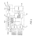
- the configuration logic circuit comprises command decoder 21, Vcc switch 22, DRAM interface refresh counter 23, direction selector 24 and multiplexers 25 and 26.
- Command detector 21 receives and decodes an instruction CMND input from an external circuit synchronously with a synchronisation signal WCK, so as to issue instructions to other circuits in the functional block.
- Vcc switch 22 controls supply of power source voltage Vcc to DRAM 30.
- DRAM interface refresh counter 23 generates signals required for the operation of DRAM 30, such as load address strobe signals, column address strobe signals, write-enable signals, output-enable signals and address signals, given from the signal supplied from command decoder 21.
- Direction selector 24 issues an instruction to receiving multiplexer 25 and sending multiplexer 26 respectively to instruct which one of adjacent functional blocks a signal should be received from, as well as which one of the adjacent functional blocks a signal should be sent to.
- Receiving multiplexer 25 selectively connects only one of input terminals of signals RECV-N, E, S and W respectively from the four adjacent functional blocks.
- the last characters of these signal names respectively denote connections with North, East, South or West adjacent blocks, and their terminals are respectively provided on the North, East, South and West sides of each functional block.
- Sending multiplexer 26 selectively connects only one of output terminals of signals XMIT-N, E, S and W respectively to the four adjacent functional blocks.
- a wafer scale IC memory having a functional block structure as described above has been reported in a paper entitled "200 Mb WAFER MEMORY" by N. MacDonald et al., in 1989 IEEE ISSCC DIGEST of TECHNICAL PAPERS, pages 240 to 241. In this report, the functional block is called a chip.
- Fig. 5 shows an enlarged partial detail view of an example of a wafer-scale IC configured in accordance with the basic embodiment of the present invention illustrated in Fig. 3(a).
- connection terminals receiving in parallel voltages from external circuits, for example, from a Vcc power supply terminal, a Vbb substrate voltage terminal, a clock (WCK) terminal and a command (CMND) terminal, provided in respective functional blocks 12A, 12B, 12C, Vietnamese are aligned in vertical lines and are doubly connected with each other in the lines by layer wiring 13 and bonding wires 17.
- a plurality of connection terminals 42 in an extra block 19′ provided below and to the outside of functional blocks 12A and 12A′ on the wafer.
- connection terminals 42 is connected to a respective one of connection terminals 14 in functional blocks 12A and 12A′ (12B), and to a respective one of external terminals 18 by wire bonding 41.
- a connection terminal 42 functions as a relay terminal between an external source and the functional blocks.
- power source voltages and signals are input in parallel to each of the functional blocks.
- Blocks 19 which are located at the periphery of wafer 11′ and are unusable as functional blocks, are provided with connecting terminals, i.e. pads, for extending the wirings, so that these pads aligned vertically are connected with each other doubly by layer wiring and by bonding wires in order to supply the power source voltage to the functional blocks 12G ⁇ , 12H ⁇ , Vietnamese aligned vertically above these unusable blocks 19.
- connecting terminals i.e. pads
- local wirings LL for sending/receiving signals between vertically adjacent functional blocks, for example, 12F and 12G
- local wirings LL′ for sending/receiving signals between the horizontally adjacent functional blocks, for example, between 12D and 12D′, and between 12E and 12E′ shown in Fig. 5.
- each functional block 20 is provided with layer wiring LL of Fig. 5 for sending/receiving signals RECV/XMIT to/from the adjacent functional blocks.
- Fig. 6 is a plan view illustrating another basic embodiment of the present invention. Elements like those found in Fig. 3(a) are designated by like reference signs. Fig. 6 is different from Fig. 3(a) only in the method of wiring bonding. As shown in Fig. 6, bonding wire 17 is cut or separated at each connection terminal 14 and the welding positions of two bonding wire ends on a connection terminal 14 are displaced from one another on the connection terminal 14.
- the layer wiring is superior in terms of its vibration-resistance characteristics, even though it suffers a problem in relation to patterning with a reticule, but on the other hand the wire bonding is superior in reliability even though it suffers a problem in relation to its vibration-resistance characteristics.
- the double wirings of an embodiment of the present invention having different failure modes, serve to improve reliability remarkably.
- branching (distributing) voltages such as power source voltages or clock signal voltage
- An embodiment of the invention can provide a wafer-scale integrated-circuit, formed on a single wafer, which has a reliable connection of wirings to each of the functional blocks in the wafer-scale IC.
- pad electrodes for commonly receiving a voltage, such as power supply voltage and clock signal, provided on each of a plurality of identical functional blocks, are connected with each other in duplicate by layered wirings and bonding wires electrically in parallel to each other.
- connection wirings failure modes are different for the respective wiring types, resulting in an increased reliability of the wafer scale integrated circuit.
- Dually connected wirings are particularly advantageous in a case in which wiring between two adjacent functional blocks is in series to the wiring of the oppositely adjacent functional blocks, i.e. the wirings for commonly supplying the power source voltage via serially-connected wirings to the functional blocks.
Landscapes
- Semiconductor Integrated Circuits (AREA)
- Internal Circuitry In Semiconductor Integrated Circuit Devices (AREA)
Applications Claiming Priority (2)
| Application Number | Priority Date | Filing Date | Title |
|---|---|---|---|
| JP1244554A JPH03106029A (ja) | 1989-09-20 | 1989-09-20 | ウエハ・スケール・ic |
| JP244554/89 | 1989-09-20 |
Publications (3)
| Publication Number | Publication Date |
|---|---|
| EP0418802A2 true EP0418802A2 (fr) | 1991-03-27 |
| EP0418802A3 EP0418802A3 (en) | 1991-05-29 |
| EP0418802B1 EP0418802B1 (fr) | 1997-02-12 |
Family
ID=17120435
Family Applications (1)
| Application Number | Title | Priority Date | Filing Date |
|---|---|---|---|
| EP90117908A Expired - Lifetime EP0418802B1 (fr) | 1989-09-20 | 1990-09-18 | Structure de conducteurs dans un circuit intégré à échelle de plaquette |
Country Status (4)
| Country | Link |
|---|---|
| US (1) | US5032889A (fr) |
| EP (1) | EP0418802B1 (fr) |
| JP (1) | JPH03106029A (fr) |
| KR (1) | KR930009015B1 (fr) |
Cited By (1)
| Publication number | Priority date | Publication date | Assignee | Title |
|---|---|---|---|---|
| EP1306898A1 (fr) * | 2001-10-29 | 2003-05-02 | Dialog Semiconductor GmbH | Sous-milliohm interconnexion sur puce |
Families Citing this family (3)
| Publication number | Priority date | Publication date | Assignee | Title |
|---|---|---|---|---|
| JP2516403B2 (ja) * | 1988-06-01 | 1996-07-24 | 富士通株式会社 | ウエハ・スケ―ル・メモリ |
| JP2585799B2 (ja) * | 1989-06-30 | 1997-02-26 | 株式会社東芝 | 半導体メモリ装置及びそのバーンイン方法 |
| US5239191A (en) * | 1990-01-19 | 1993-08-24 | Kabushiki Kaisha Toshiba | Semiconductor wafer |
Family Cites Families (4)
| Publication number | Priority date | Publication date | Assignee | Title |
|---|---|---|---|---|
| JPS57164651A (en) * | 1981-03-20 | 1982-10-09 | Fujitsu Ltd | Control system for switchboard |
| JPS60239051A (ja) * | 1984-05-11 | 1985-11-27 | Mitsubishi Electric Corp | 半導体装置 |
| GB2177825B (en) * | 1985-07-12 | 1989-07-26 | Anamartic Ltd | Control system for chained circuit modules |
| WO1989012320A1 (fr) * | 1988-06-01 | 1989-12-14 | Anamartic Limited | Circuits integres a l'echelle d'une tranche |
-
1989
- 1989-09-20 JP JP1244554A patent/JPH03106029A/ja active Pending
-
1990
- 1990-09-11 KR KR1019900014311A patent/KR930009015B1/ko not_active Expired - Fee Related
- 1990-09-18 EP EP90117908A patent/EP0418802B1/fr not_active Expired - Lifetime
- 1990-09-20 US US07/585,515 patent/US5032889A/en not_active Expired - Lifetime
Cited By (3)
| Publication number | Priority date | Publication date | Assignee | Title |
|---|---|---|---|---|
| EP1306898A1 (fr) * | 2001-10-29 | 2003-05-02 | Dialog Semiconductor GmbH | Sous-milliohm interconnexion sur puce |
| US6569758B2 (en) | 2001-10-29 | 2003-05-27 | Dialog Semiconductor Gmbh | Sub-milliohm on-chip interconnection |
| US7291551B2 (en) | 2001-10-29 | 2007-11-06 | Dialog Semiconductor Gmbh | Sub-milliohm on-chip interconnection |
Also Published As
| Publication number | Publication date |
|---|---|
| EP0418802A3 (en) | 1991-05-29 |
| JPH03106029A (ja) | 1991-05-02 |
| US5032889A (en) | 1991-07-16 |
| KR930009015B1 (ko) | 1993-09-18 |
| KR910007121A (ko) | 1991-04-30 |
| EP0418802B1 (fr) | 1997-02-12 |
Similar Documents
| Publication | Publication Date | Title |
|---|---|---|
| KR100283030B1 (ko) | 반도체 장치의 레이 아웃 구조 | |
| US6858472B2 (en) | Method for implementing selected functionality on an integrated circuit device | |
| JP2585799B2 (ja) | 半導体メモリ装置及びそのバーンイン方法 | |
| US5691949A (en) | Very high density wafer scale device architecture | |
| US20020163019A1 (en) | Interconnect substrate with circuits for field-programmability and testing of multichip modules and hybrid circuits | |
| US6991970B2 (en) | Method and apparatus for circuit completion through the use of ball bonds or other connections during the formation of semiconductor device | |
| WO1991015853A1 (fr) | Architecture d'un dispositif de la taille d'une tranche a tres haute densite | |
| EP0418802B1 (fr) | Structure de conducteurs dans un circuit intégré à échelle de plaquette | |
| CN1233841A (zh) | 测试在一个晶片上的多个存储器芯片的装置 | |
| EP0345162B1 (fr) | Dispositif intégré à l'échelle de tranche | |
| JPH0661298A (ja) | 半導体集積回路装置 | |
| US5644526A (en) | Integrated circuit with improved immunity to large metallization defects | |
| KR100541798B1 (ko) | 반도체 장치의 테그 패턴 형성방법 | |
| JPH0158662B2 (fr) | ||
| US7199460B2 (en) | Semiconductor device and method of manufacturing the same | |
| WO1989012320A1 (fr) | Circuits integres a l'echelle d'une tranche | |
| EP0413590A2 (fr) | Dispositif de circuit intégré à échelle de plaquette | |
| JPS58202547A (ja) | 集積回路装置 | |
| JPH04207051A (ja) | ウエハスケールインテグレーションデバイスの製造方法 | |
| WO1985001390A1 (fr) | Tranche | |
| EP0403898A2 (fr) | Dispositif de circuit intégré semi-conducteur à l'échelle d'une tranche et procédé pour former les lignes d'interconnexions disposées entre les puces d'un dispositif de circuit intégré semi-conducteur à l'échelle d'une tranche | |
| JP2006216970A (ja) | 半導体パッケージ | |
| JPS61104639A (ja) | 半導体集積回路装置 | |
| JPS63202938A (ja) | マスタ−スライス型半導体装置 | |
| JPH05274866A (ja) | 半導体装置 |
Legal Events
| Date | Code | Title | Description |
|---|---|---|---|
| PUAI | Public reference made under article 153(3) epc to a published international application that has entered the european phase |
Free format text: ORIGINAL CODE: 0009012 |
|
| AK | Designated contracting states |
Kind code of ref document: A2 Designated state(s): DE FR GB |
|
| PUAL | Search report despatched |
Free format text: ORIGINAL CODE: 0009013 |
|
| AK | Designated contracting states |
Kind code of ref document: A3 Designated state(s): DE FR GB |
|
| 17P | Request for examination filed |
Effective date: 19911007 |
|
| 17Q | First examination report despatched |
Effective date: 19940328 |
|
| GRAG | Despatch of communication of intention to grant |
Free format text: ORIGINAL CODE: EPIDOS AGRA |
|
| GRAH | Despatch of communication of intention to grant a patent |
Free format text: ORIGINAL CODE: EPIDOS IGRA |
|
| GRAH | Despatch of communication of intention to grant a patent |
Free format text: ORIGINAL CODE: EPIDOS IGRA |
|
| GRAA | (expected) grant |
Free format text: ORIGINAL CODE: 0009210 |
|
| RBV | Designated contracting states (corrected) |
Designated state(s): GB |
|
| REG | Reference to a national code |
Ref country code: DE Ref legal event code: 8566 |
|
| AK | Designated contracting states |
Kind code of ref document: B1 Designated state(s): GB |
|
| PLBE | No opposition filed within time limit |
Free format text: ORIGINAL CODE: 0009261 |
|
| STAA | Information on the status of an ep patent application or granted ep patent |
Free format text: STATUS: NO OPPOSITION FILED WITHIN TIME LIMIT |
|
| 26N | No opposition filed | ||
| REG | Reference to a national code |
Ref country code: GB Ref legal event code: IF02 |
|
| PGFP | Annual fee paid to national office [announced via postgrant information from national office to epo] |
Ref country code: GB Payment date: 20050914 Year of fee payment: 16 |
|
| GBPC | Gb: european patent ceased through non-payment of renewal fee |
Effective date: 20060918 |
|
| PG25 | Lapsed in a contracting state [announced via postgrant information from national office to epo] |
Ref country code: GB Free format text: LAPSE BECAUSE OF NON-PAYMENT OF DUE FEES Effective date: 20060918 |