EP0419216A2 - Vorrichtung für optische Datenübertragung mit parallelen Kanälen für eine lineare Anordnung von optischen Elementen - Google Patents
Vorrichtung für optische Datenübertragung mit parallelen Kanälen für eine lineare Anordnung von optischen Elementen Download PDFInfo
- Publication number
- EP0419216A2 EP0419216A2 EP90310209A EP90310209A EP0419216A2 EP 0419216 A2 EP0419216 A2 EP 0419216A2 EP 90310209 A EP90310209 A EP 90310209A EP 90310209 A EP90310209 A EP 90310209A EP 0419216 A2 EP0419216 A2 EP 0419216A2
- Authority
- EP
- European Patent Office
- Prior art keywords
- optical
- light
- transmission line
- transmission
- wiring lines
- Prior art date
- Legal status (The legal status is an assumption and is not a legal conclusion. Google has not performed a legal analysis and makes no representation as to the accuracy of the status listed.)
- Granted
Links
Images



Classifications
-
- H—ELECTRICITY
- H04—ELECTRIC COMMUNICATION TECHNIQUE
- H04B—TRANSMISSION
- H04B10/00—Transmission systems employing electromagnetic waves other than radio-waves, e.g. infrared, visible or ultraviolet light, or employing corpuscular radiation, e.g. quantum communication
- H04B10/25—Arrangements specific to fibre transmission
- H04B10/2507—Arrangements specific to fibre transmission for the reduction or elimination of distortion or dispersion
-
- G—PHYSICS
- G02—OPTICS
- G02B—OPTICAL ELEMENTS, SYSTEMS OR APPARATUS
- G02B6/00—Light guides; Structural details of arrangements comprising light guides and other optical elements, e.g. couplings
- G02B6/24—Coupling light guides
- G02B6/42—Coupling light guides with opto-electronic elements
- G02B6/43—Arrangements comprising a plurality of opto-electronic elements and associated optical interconnections
-
- H—ELECTRICITY
- H10—SEMICONDUCTOR DEVICES; ELECTRIC SOLID-STATE DEVICES NOT OTHERWISE PROVIDED FOR
- H10W—GENERIC PACKAGES, INTERCONNECTIONS, CONNECTORS OR OTHER CONSTRUCTIONAL DETAILS OF DEVICES COVERED BY CLASS H10
- H10W72/00—Interconnections or connectors in packages
- H10W72/50—Bond wires
- H10W72/531—Shapes of wire connectors
- H10W72/536—Shapes of wire connectors the connected ends being ball-shaped
-
- H—ELECTRICITY
- H10—SEMICONDUCTOR DEVICES; ELECTRIC SOLID-STATE DEVICES NOT OTHERWISE PROVIDED FOR
- H10W—GENERIC PACKAGES, INTERCONNECTIONS, CONNECTORS OR OTHER CONSTRUCTIONAL DETAILS OF DEVICES COVERED BY CLASS H10
- H10W72/00—Interconnections or connectors in packages
- H10W72/50—Bond wires
- H10W72/531—Shapes of wire connectors
- H10W72/5363—Shapes of wire connectors the connected ends being wedge-shaped
-
- H—ELECTRICITY
- H10—SEMICONDUCTOR DEVICES; ELECTRIC SOLID-STATE DEVICES NOT OTHERWISE PROVIDED FOR
- H10W—GENERIC PACKAGES, INTERCONNECTIONS, CONNECTORS OR OTHER CONSTRUCTIONAL DETAILS OF DEVICES COVERED BY CLASS H10
- H10W72/00—Interconnections or connectors in packages
- H10W72/50—Bond wires
- H10W72/541—Dispositions of bond wires
- H10W72/5445—Dispositions of bond wires being orthogonal to a side surface of the chip, e.g. parallel arrangements
-
- H—ELECTRICITY
- H10—SEMICONDUCTOR DEVICES; ELECTRIC SOLID-STATE DEVICES NOT OTHERWISE PROVIDED FOR
- H10W—GENERIC PACKAGES, INTERCONNECTIONS, CONNECTORS OR OTHER CONSTRUCTIONAL DETAILS OF DEVICES COVERED BY CLASS H10
- H10W72/00—Interconnections or connectors in packages
- H10W72/90—Bond pads, in general
- H10W72/931—Shapes of bond pads
- H10W72/932—Plan-view shape, i.e. in top view
Definitions
- the present invention is directed to optical data transmission systems and, more particularly, to a parallel optical data transmission device which has an array of solid-state light-emitting elements, such as semiconductor lasers, mounted on the same substrate using a hybrid IC technology and transmits optical information signals in a parallel manner.
- a parallel optical data transmission device which has an array of solid-state light-emitting elements, such as semiconductor lasers, mounted on the same substrate using a hybrid IC technology and transmits optical information signals in a parallel manner.
- optical transmission technology has been introduced to fulfill the demand of a greater amount of, and faster transmission of, intercomputer information signals. Basically, it is undeniable that the optical transmission technology is given an important role in the highly advanced computer communication network in light of its advantages, such as noninductiveness, wide-band characteristic and high-speed transmission of the transmission lines. Those skilled in the art do not however believe that a single optical transmission line employed among the existing communication machines can sufficiently cope with transmission of high rate, digital optical information signals.
- the key to overcome these problems is the parallel optical data transmission technology.
- Data communications among computer terminals, known as “workstations,” are normally executed with digital data having a selected number of bits as a data unit, so that the parallel optical transmission scheme is just the “best casting.”
- the parallel optical transmission scheme With the parallel optical transmission scheme, the signal transmission capacity and the signal transfer rate can be significantly increased; in addition, it is possible to in principle eliminate the need for extra circuit structures, such as parallel-to-serial converters and time-division multiplexing/demultiplexing devices, unlike in the case of serial transmission using a single transmission line path, and, at the same time, to minimize the total required buffer memory. This can reduce the burden on the hardware structure.
- the parallel optical transmission technology which is expected to be developed, actually has several unsettled issues.
- One of these issues is realization of perfect unification of effective wire lengths at the electric wiring portions of individual signal transmission channels.
- Another issue is to deal with reduction in effective signal margin caused by the inductive cross talk between adjoining electric signal transmission channels and/or ground potential noise and elimination of the non-uniform characteristic impedance.
- the present invention is addressed to a specific optical data transmission device which has first and second mutually spaced base plate portions having electrical signal terminals formed at predetermined intervals.
- An array of a preselected number of light-emitting elements are provided on the first base plate portion and are arranged at intervals smaller than the intervals of the signal terminals.
- An array of photosensitive devices equal in number to the light-emitting devices are provided on the second base plate portion and are arranged at intervals smaller than the intervals of the signal terminals.
- An optical coupling section is provided to optically couple the first and second base plate portions.
- the optical coupling section has parallel transmission lines for permitting independent transmission of optical signals between the light-emitting devices and the photosensitive devices.
- a transfer delay in the transmission of optical signals between the light-emitting devices and the photosensitive devices via the parallel transmission lines is compensated for by making the total electric transmission line lengths of the parallel transmission lines running through the electrical signal terminals, the light-emitting devices and the photosensitive devices essentially equal to one another.
- a 5-channel arrayed optical data transmission device in accordance with one embodiment of the present invention is presented which performs parallel optical transmission.
- This "arrayed" optical data transmission device has an optical signal emitting unit 10, an optical reception unit 20 that is spatially distant from the unit 10, and a parallel optical transmission cable 30 provided therebetween.
- the optical signal emitting transmission unit 10 has an insulative substrate 12 to be coupled to an array of optical semiconductor elements 14 that emit light modulated to represent optical information signals.
- These elements 14 may be known types of light-emitting devices, such as light-emitting diodes, semiconductor laser devices, or the like, as will be explained in detail later.
- the optical reception unit 20 has an insulative substrate 22 to be coupled to an array of semiconductor photosensitive elements 24 that serve as "photodetectors" for detecting optical signals externally supplied thereto. These spatially separated substrates 12 and 22 are coupled with each other by means of the parallel optical transmission cable 30.
- the output optical signals of the light-emitting elements 14 are sent via the cable 30 to the semiconductor photosensitive elements 24 mounted on the substrate 22. Since this embodiment involves a 5-channel optical transmission, the optical cable 30 essentially consists of five parallel fibers bundled together.
- the optical signals emitting substrate 12 is securely attached onto a plate 16 of high conductivity, which may be made of copper or aluminum.
- the plate 14 serves as a "heat discharger" of the optical signals emitting substrate 12; it also acts as a ground electrode.
- An array of the optical signals emitting elements 14 are securely mounted on the ground electrode plate 16.
- the optical signals emitting substrate 12 has signal input pads A1, A2, A3, A4 and A5 formed at the opposite edge portion. These signal input pads A are electrically connected on the substrate 12 to the optical signals emitting elements 14 by means of connection wires or lines 18-1, 18-2, 18-3, 18-4 and 18-5. With the electrical wiring arrangement, an electrical input signal externally supplied to each of the signal input pads-such as a laser drive signal representing information to be transmitted-is supplied to a corresponding element 14i, and then converted into an optical signal indicative of the information.
- a laser drive signal representing information to be transmitted-is supplied to a corresponding element 14i
- the other substrate e.g., optical signals reception substrate 22, is similar in its arrangement to the optical signals emitting substrate 12. More specifically, the substrate 22 is attached onto a ground electrode plate 26, on which an array of the photodetector elements 24 are securely mounted.
- the substrate 22 has electrical signal output pads B1, B2, B3, B4 and B5 which are formed at the opposite edge portion; these pads B are electrically connected in a one-to-one correspondence manner to the photodetectors 24 by means of connection wires or lines 28-1, 28-2, 28-3, 28-4 and 28-5. Accordingly, optical signals transferred over the 5-channel optical transmission cable 30 from the light-emitting elements 14 are converted into electrical signals by corresponding photodetectors 24, then are supplied to the corresponding signal output pads B associated therewith.
- the optical signals emitting elements 14 may be GalnAsP/lnP- or GaAtAS/GaAs-based light-emitting diodes (LEDs) or semiconductor lasers; the photodetectors 24 may be PIN photodiodes made of a semiconductor material corresponding to that of the elements 14.
- the optical transmission cable 30 may be optical fibers of quartz bundled in parallel at pitches of about 250 micrometers. As the insulative substrates 12 and 22, A1 2 0 3 plates about 100 micrometers thick are used.
- the wiring on the substrates 12 and 22 including the signal input pads A and signal output pads B is made using a well-known patterning technique; for example, the pitches of the pads A and B are 0.5 to 2.5 millimeters and the pitches of the light-emitting devices 14 and the light-receiving devices 24 are 0.25 millimeter.
- the width of the lines 18 and 28 on the substrates may be 100 micrometers.
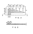
- the whole back of each of the substrates 12 and 22 is metallized with Au/Cu to have a thickness of 100 nanometers for each, as indicated by reference numeral "19" in Figure 3, thus providing a microstrip line structure having a characteristic impedance of 50 ohms.
- the wiring lines 18-1, 18-2, 18-3, 18-4, and 18-5 are bent in a stair-step shape with the lengths sequentially varying, in such a manner that the line 18-1 for the rightmost signal input pad A1 is the longest in terms of the signal transmission line length and that the line 18-5 for the leftmost signal input pad A5 is the shortest in terms of the total line length, as shown in Figure 1.
- wiring lines 28-1, 28-2, 28-3, 28-4, and 28-5 on the substrate 22 of the optical signals reception unit 20 are bent in a stair-step shape, with thin layers sequentially varying, in such a manner that the line 28-1 for the rightmost signal output pad B1 is the shortest and the line 28-5 of the leftmost signal output pad B5 is longest in terms of the total line length.
- the longest on-substrate transmission line 18-1 of the optical signals emitting unit 10 is associated with the shortest on-substrate transmission line 28-1 of the optical signals reception unit 20; while, the shortest transmission line 18-5 of the unit 10 is associated with the longest transmission line 28-5 of the other unit 20. Therefore, their total lengths of electrical transmission line paths become absolutely equal to one another and constant. In other words, the lengths of the effective transmission lines between the pads A as signal input terminals and the pads B as signal output terminals become completely equal to one another.
- FIG. 2 presents a detailed illustration of the "sequentially lengths-varying stair-step bending" arrangement for the on-substrate transmission lines 18.
- the pitches between the signal input pads A1, A2, A3, A4 and A5 are indicated by “a”
- the signal transmission line path lengths L1, L2, L3, L4 and L5 of the lines 18-1, 18-2, 18-3, 18-4 and 18-5 are expressed as follows:
- the signal transmission line path lengths L1', L2', L3', L4' and L5' of the electrical lines 28-1, 28-2, 28-3, 28-4 and 28-5 of the optical reception unit 20 having the reverse "sequentially lengths-varying stair-step bending" arrangement are expressed as follows:
- phase-shifted optical signals are sent via the optical transmission cable 30 to the optical signals reception unit 20, and are then converted again by the photosensitive elements 24 serving as photodetectors to be "reconstructed" into the original electrical signals.
- the mutual phase shifting of the reconstructed electrical signals is automatically compensated for one-by-one by the "reverse phase shifting" while the signals are being transmitted through the lines 28-1 to 28-5 which are bent with the lengths sequentially varying, so that the signals have the exactly same phase when they reach the signal output pads B1 to B5.
- transmitting digital data signals using the parallel optical data transmission device can compensate 100% for the distribution of the transfer speed for every data bit.
- the bit delay during transfer can be suppressed, an extra circuit structure to cope with the signal delay is totally unnecessary, thus ensuring high-speed transmission of parallel information signals in a communication system with the smallest additional circuit structure.
- cross talk between signals caused during transmission is quite unlikely to be superimposed on the transmitted signals, because the signal cross talk itself delays or advances with time for each of the transmission lines on the substrate.
- Such a shift of the cross talk itself brings about an unexpected advantage that permits data discrimination with a clock signal as a reference and elimination of a cross talk component of data preceding and following the discriminated data based thereon. it is therefore possible to improve the effective signal margin in parallel information transmission and significantly increase the transmission efficiency. This can contribute to improving the quality of transmission signals.
- the on-substrate wiring lines 18 and 28 are formed in a stair-step shape according to the concept of the "sequentially lengths-varying stair-step bending" arrangement; however, the shape is not restrictive to this type but may take a wave form or a linear track form without abandoning the basic concept of the present invention.
- a hybrid semiconductor integrated device employed in a parallel optical data transmission device in accordance with the second embodiment of the present invention is generally designated by reference numeral "110."
- This hybrid integrated device 110 is an optical transmitter having an array type semiconductor laser section 112 and a transmission line path substrate 114, associated with a drive IC section (not visible in Figure 4) of the laser section, both located on a mounting substrate 116.
- This device may be considered as the aforementioned optical signals emitting substrate 12 of the first embodiment having the arrayed light-emitting elements 14.
- the mounting substrate 116 may be a ceramic plate of high heat-conductivity having a metallized surface or a metal plate; this substrate 116 will be called “mother board” or “main board” in the following description.
- a semiconductor laser section 112 is securely mounted on a certain edge section of the main board 116.
- the laser section 112 has a selected number of semiconductor laser devices 118 arranged in an array. According to the illustrated embodiment, four semiconductor lasers 118a, 118b, 118c and 118d are arranged in parallel so as to constitute a 4-channel array type laser section. Each of these semiconductor lasers 118 has a wire bonding contact face defined on its top.
- GaN gallium-indium-arsenic-phosphorus/indium-phosphorus
- signal transmission lines 120a, 120b, 120c and 120d to be connected to a drive circuit are formed in parallel by a patterning technique. These wiring lines 120 define square-shaped pad patterns at those portions which terminate at an edge portion of the substrate 114.
- the 4-channel array type laser section 112 and the drive-signals transmission line substrate 114 therefor are arranged adjacent to each other, with a predetermined distance therebetween, on the main board 116.
- the distances or pitches between the semiconductor lasers 118 in the laser section 112 are substantially identical to the mutual distances between the drive-signals transmission lines 120 for the semiconductor laser devices.
- the array type laser section 112 has wire bonding regions of the ground lines, which are formed on the same side as the wire bonding tops, as will be described below in greater detail.
- the array type laser section 112 has an elongated rectangular-shaped InP substrate layer 130 of N type conductivity.
- An N type InP buffer layer 132, undoped GalnAsP active layers 134 and P type InP cladding layer 136 are sequentially laminated on the substrate layer 130.
- the active layers 134 are buried in a stripe shape by the cladding layer 136 by means of a well-known patterning process.
- a first metal layer 138 serving as a signal line electrode is formed on the top surface of the laser section 112, and a second metal layer 140 serving as a ground electrode is formed on the bottom surface of the laser section 112.
- Parallel separation grooves 142 are formed at fixed intervals of a constant distance in the P type InP cladding layer 136 and signal line electrode layer 138.
- the separation grooves 142 are deep enough to penetrate the layers 138 and 136.
- the separation grooves 142 define the semiconductor laser portions 118a, 118b, 118c and 118d, and ground line bonding portions 144a, 144b, 144c, 144d and 144e, which do not have the active layers 134.
- portions 118 will be called the “bonding mesa portions” hereinafter; they may also be called the “ground mesa portions,” or “dummy mesa portions.”
- the semiconductor laser sections 118 and the ground line bonding portions 144 are alternately arranged along the length of the laser substrate layer 130-this alternate array structure should be well understood referring to Figure 7-thereby to provide the substrate-grounded type 4-channel array laser structure.
- connection terminal of a substrate-grounded electrode layer 140 is indicated by “Gs.”
- “Ta,” “Tb,” “Tc” and “Td” are used to represent drive signal supply terminals of the laser devices 118a, 118b, 118c and 118d of the 4-channel array laser section 112.
- the ground connection terminals of the bonding mesa portions 144a to 144e are denoted by “G1" through “G5,” respectively.
- Ground lines 146a, 146b, 146c, 146d and 146e running in parallel are additionally formed on the top surface of the transmission line substrate 114 in association with the terminals G1 to G5.
- These ground lines 146 and the aforementioned drive-signals transmission lines 120a to 120d are alternately arranged, as shown in Figure 6.
- each drive-signals transmission line 120i is electrically and magnetically shielded on both sides by two ground lines 146 that are each neighboring thereto.
- ground bonding wires 148 are marked black simply for the purpose of providing a visual distinction-each of the drive signals transmission bonding wires 122 is held on its both sides by two ground bonding wires 148 also in the "array" of bonding wires between the array type semiconductor laser section 112 and transmission line substrate 114; each bonding wire 122i can therefore be electrically and magnetically shielded from the others, adjoining bonding wires 122.
- the present inventors produced several samples of the actual device employing the above-described structure.
- the substrate of the array type semiconductor laser section 112 of one sample was approximately 250 micrometers long (i.e., the laser resonator length) and approximately 1200 micrometers wide.
- Eight separation grooves 142 of 25 micrometers wide were formed at equal intervals of about 100 micrometers, thereby defining the laser devices 118 of 100 micrometers wide and ground mesa portions (dummy mesa portions) 144 of 100 micrometers wide arranged alternately.
- the additional ground wires 146 and the ground connecting bonding wires 148 well serve as shield lines or "electromagnetic barriers" for each transmission line 120 and its bonding wire 122 from the following fact.
- the DC component of the ground wires 146 was completely eliminated by the PN reverse bias junction at the N type layer 132 and P type layer 136, and only a slight AC component was coupled between the adjoining ground terminals G1, G2, ..., G5 through the capacitor at the PN reverse bias junction.
- the 4-channel array type laser section 112 having the substrate-grounded type structure as used in the above embodiment can be replaced with the one having a "substrate-insulating type" laser structure as shown in Figure 7.
- the laser substrate layer is comprised of an InP layer 150 of N type, P type or I type (semi-insulative type).
- An N type InP buffer layer 152 is formed on this InP layer 150.
- Parallel separation grooves 142 are formed on the top surface of the InP buffer layer 152 as in the structure shown in Figure 5, thereby defining alternately-arranged laser device regions (signal line mesa portions) 118a, 118b, 118c and 118d and ground mesa portions (dummy mesa portions) 154a, 154b, 154c, 154d and 154e.
- P type InP cladding layers 136 are formed only in the laser device regions. The selective formation of these P type cladding layers 136 can be made by selective diffusion of P type impurities and selective growth of a P type InP or N type InP layer.
- the N type InP layer 152 may have the cross-sectional structure shown in Figure 7 by forming the P type InP layer 136, then selectively removing it. Step-like configurations produced in this case on the surface of the resultant structure are merely 1 or 2 micrometers high, which are practically insignificant.
- the other cross-sectional structures are substantially identical to those of the structure shown in Figure 5.
- the electrode layer 140 on the bottom side serves as a metal layer formed by metalization for securely connecting the array type laser section 112 on the main board 116, and that this metal layer may be electrically separated or insulated from the main board 116.
- the electrical connection between the 4-channel array type laser section 112 having the substrate-insulating type structure shown in Figure 7 and the transmission line path substrate 114 is basically the same as the one provided in the previous embodiment, and is made using the alternately-arranged drive-signal bonding wires 122 and ground connecting bonding wires 148.
- the present inventors prepared some samples of the device having the array type laser section 112' in Figure 7 mounted on the main board 116 and confirmed the effect of preventing "cross-talk" between adjoining channels as in the previous case.
- the array type semiconductor laser section 112 of one sample was made to have the aforementioned size. Given the bonding wires 122 and 148 are sufficiently longer than the wavelength of the electromagnetic wave, the characteristic impedance Zo of signal lines between the laser section 112 and the transmission line substrate 114 becomes approximately 550 ohms:
- the bonding wires are formed sufficiently shorter than the length of the electromagnetic wave, making the value of the characteristic impedance smaller than the computed value. It will therefore be recommendable for actual devices that a careful consideration be made in accordance with the wire length and the shape of the loop and that the optimal adjustment of the device size or the like be conducted when needed.
- the ground connection bonding wires 148 arranged alternately with respect to the former wires 122 are provided to the signal transmission lines between the array type laser section 112 or 112 and the transmission line substrate 114 mounted on the main board 116, whereby the wires of the ground line including the bonding wire connecting portion can substantially be rendered to completely "run in parallel" with the wires of the signal transmission lines. It is thus possible to reduce or eliminate the adverse affect of a variation in distance or interval between the signal line wires and ground surface of the mounting substrate at the electrical connection between the functional blocks of the hybrid integrated device on the signal transmission characteristic.
- the functional elements-or function blocks- can be made independent from one another while being freed from a consideration of deterioration of the characteristic, thus permitting free designing of the transmission lines. This can greatly contribute to making the best use of the original advantages of the hybrid integrated device.
- the additional ground connection bonding wires 148 can successfully provide electromagnetic shielding of each drive-signal bonding wire 122. This can minimize the unbalanced impedance likely to occur at the electrical connecting portions between the hybrid integrated functional devices and/or the generation of cross talk between channels in the array type light-emitting device. As a consequence, it is possible to significantly improve the high-frequency signal transmission performance in a frequency band of several gigahertz. Manufacturers of hybrid integrated devices should be very happy to know that the above technical advantages can be obtained without any inconvenience, such as complication of the structure or adverse influence on the manufacturing process.
- a semiconductor laser device which is preferably used in a parallel optical data transmission system is illustrated in Figure 8 as the third embodiment of the present invention; this laser device is generally designated by reference numeral "210."
- the semiconductor laser device 210 is used as one-channel optical signal generating unit with an optical output monitor, which is the most basic structure.
- the optical output monitor is necessary in order to provide an abnormal status detection for either an output-level variation compensating electric feedback control or a prevention of device deterioration.
- a photodiode acting as the detection element therefor is provided in the semiconductor laser device 210.
- an optimized electrical signal transmission line path for a optical signal emitting laser and a laser-output monitoring photodiode is provided which is never “interfered” with an optical coupling line paths between the laser and the photodiode, as will be described in detail hereinafter.
- the semiconductor laser device 210 has an insulative substrate 212.
- the substrate 212 is securely mounted on a highly-conductive plate 214, which is made of, for example, a high heat-conductive metallized ceramic plate or a copper plate.
- the plate 214 serves as a heat-discharging member for the substrate 212; simultaneously, it acts as a ground electrode.
- a semiconductor laser 216 and monitoring photodiode 218 are stably mounted on the heat-discharging plate 214, as illustrated.
- the whole back surface of the substrate 212 is metallized to form a ground electrode layer 220, as shown in Figure 9.
- the substrate 212 has an electrical transmission line 224 of, for example, a linear shape, on its insulative top surface.
- the transmission line 224 is connected at one end to a signal input terminal 226, and connected at the other end thereof to the laser 216 by means of a bonding wire 228.
- the characteristic impedance of the transmission line 224 is adjusted to be 50 ohms in cooperation with the metallized ground layer 220, thus suppressing the undesired power reflection at the coupling section of the transmission line 224.
- an electrical laser drive signal is externally supplied to the terminal 226, this signal is sent via the signal transmission line 224 and bonding wire 228 to the laser device 21.
- the laser device 216 produces an optical information signal.
- the electrical information signal input to the terminal 226 is converted into a corresponding optical information signal 230, which is in turn sent out to, for example, an optical transmission cable (not shown in Figures 8 and 9) coupled to the terminal 226.
- the laser-connecting end portion of the substrate 212 has an inclined face 238 with a predetermined angle of e in order to prevent a so-called "near-end reflection.”
- the semiconductor laser 216 when applied with an external reflection component of the light being emitted by itself, it creates a state in which a composite resonance mode mixed and thus produces the undesired phenomenon, such as fluctuation of the optical output or generation of excess noise.
- the inclination angle 8 should be determined in careful consideration of the optical coupling efficiency, and is set to a specific value that can best prevent the near-end reflection. In our samples, the inclination angle 6 was selected to be 15° with the interval between the laser device 216 and the end of the line 224 set to 300 micrometers.
- the laser-output monitoring photodiode 218 located away from the laser device 216 on the heat-discharging plate 214 is optically coupled with the laser 216 by an optical transmission line 232 functioning as an optical waveguide running inside the insulative substrate 212.
- this optical transmission line 232 consists of a part overlapping the electrical transmission line 224 and a bent part subsequent therefrom.
- a part of output light of the laser device 216 is led through the optical transmission line 232 along the direction of the arrow 234 to enter the monitoring photodiode 218.
- the photodiode 218 has a monitor output terminal 236 where an electrical monitor signal Sm representing the amount of the monitored output light appears.
- the length of the connecting boding wire 228 used for the semiconductor laser device 216 can well eliminate obstructions, such as reduction in signal converting efficiency and/or deterioration of the high-frequency signal waveform originating from a variation in inductance involved in the transmission of high-frequency signals or mismatching of the characteristic impedance. As a result, it is possible to improve the performance of transmitting high-frequency signals in the parallel optical data transmission device.
- the length of the laser-connecting bonding wire 228 could be set in a range of 200 to 300 micrometers, and the allowable high frequency band in this case could be improved to 10 gigahertz or greater.
- the optical coupling between the laser 216 and laser-output monitoring photodiode 218 is made exclusively by the optical transmission line 232, and no bonding wires are involved therein; this can reduce the spatial area occupied by or required for the optical coupling, particularly, the lateral width required. Such reduction in the occupying area can progress application of a laser device to a parallel optical data transmission system having a multi-channel structure, like the previous embodiments, as well as can enhance the efficiency of monitoring the optical output.
- the semiconductor laser device 216 is a GalnAsP/lnP laser and its oscillation wavelength is approximately 1.3 micrometers.
- the insulative substrate 212 is a Si0 2 plate 5 millimeters long along the line 224 and 150 micrometers thick; the heat-discharging substrate 214 was a 5-millimeter thick copper plate which had its surface gold-plated about 2 micrometers.
- the laser device 216 and diode 218 were mounted on the substrate 214 through a heat sealing sequentially using an AuSi eutectic alloy and an AuSn eutectic alloy.
- the electric signal transmission line 224 formed on the Si0 2 substrate 212 is a microstrip line, such as Au/Cr or Au/Pt/Ti, 3 to 5 micrometers thick and 250 micrometers wide, and exhibited a transmission line impedance of 50 ohms in forming the ground electrode layer 220 on the back of the substrate 220.
- the transmission line 224 and the laser device 216 were electrically connected by the bonding wire 228 having a diameter of 25 micrometers and a length of 300 micrometers.
- the signal input terminal 226 of the microstrip transmission line 224 was formed by pressure-bonding the conductor of the core of a connector for a coaxial cable.
- the optical transmission line 232 was formed by doping, for example, 20 % of an additive, such as Ge0 2 or P 2 0 5 , in the Si0 2 substrate 212 and locally increasing the substrate reflection factor of the transmission line region.
- the resultant optical transmission line was measured to be 50 micrometers deep from the top surface of the Si0 2 substrate 212, 20b micrometers thick and 50 micrometers wide.
- the light receiving angle was 30°.
- the center curvature of the bent portion was 1 millimeter, and the distance overlapping the microstrip transmission line 224 was 800 micrometers.
- This sample had a small optical wave-guide loss of 2 to 3 dB as a whole and showed a good optical-output monitoring performance.
- With the normal semiconductor laser 216 having a thickness of about 100 micrometers, when the diode 218 was mounted on the same surface, the height of the optical waveguide 232 with respect to the laser emitting end was well controlled.
- Figures 8 through 10 may be modified as illustrated in Figure 11.
- Figure 11 the same reference numerals as used for the constituents in Figure 8 are used to denote the identical or corresponding elements, thus omitting their description for the sake of descriptive simplification.
- an optical fiber 250 serving as an optical transmission line is employed in place of the buried waveguide 232 shown in Figure 8.
- the optical fiber 250 which is buried in the insulative mounting substrate 212, typically has an outer diameter of 125 micrometers, a core diameter of 50 micrometers and a light-receiving angle of 25 ⁇ .
- the substrate 212 may be an Si0 2 plate or A1 2 0 3 plate. This arrangement requires no additive doping step for forming the buried optical waveguide and eliminates the need for a permeable material for the dielectric substrate 212, thus relaxing the manufacturing conditions and reducing the manufacturing cost. Accordingly, the applicability of the present invention can be expanded.
- a semiconductor laser device for use in a multi-channel parallel optical data transmission device is designated by reference numeral "250," which can be considered as the previous laser device 210 developed have a multi-channel structure.
- a heat-discharging substrate 252 Mounted on a heat-discharging substrate 252 are an array of semiconductor laser 256, an array of photodiodes 258 and a laser driving IC 260.
- an insulative substrate 254 On an insulative substrate 254 are formed five parallel-running electrical transmission lines 262-1, 262-2, 262-3, 262-4 and 262-5. These signal transmission lines 262 provide electrical connection between the semiconductor laser array 256 and the laser driving IC 260.
- Formed in the insulative substrate 254 are five bending optical transmission lines 264-1, 264-2, 264-3, 264-4 and 264-5 as buried optical waveguides for optically coupling the semiconductor laser array 256 to the optical-output monitoring diode array 258.
- the laser devices 256 are arranged at equal intervals of 500 micrometers.
- the monitoring photodiodes 258 are arranged at equal intervals of 500 micrometers.
- the laser driving IC 260 has a driver 266 and an laser-output monitoring comparator/detector 268 electrically associated with each other.
- the driver 266 has signal input pads C1, C2, C3, C4 and C5 at one end and connection pads 270 at the opposite end.
- Each of the electrical transmission lines on the insulative substrate 254 has one end connected to a corresponding connection pad 270 by a bonding wire 272, and has the other end connected to a corresponding laser device 256 by a bonding wire 274. Accordingly, in a channel C1, for example, the drive signal is sent to a corresponding one of the laser devices 256 via the transmission line 262-1 and the bonding wires provided thereto, and light is emitted from this laser device.
- the semiconductor laser 256 are optically coupled independently to the laser-output monitoring diodes 258 via the optical transmission lines or the buried wave-guides 264-1, 264-2, 264-3, 264-4 and 264-5, respectively. Part of the optical output of each laser 256 is therefore led into an associated one of the monitoring diodes 258 by a corresponding buried waveguide 264-i. Since the diodes 258 are electrically connected to connection pads 276 of the monitoring comparator/detector circuit section 268 by the bonding wires 274, electrical light-monitoring signals are transferred to the circuit section 268.
- highest-density devices and circuits can be mounted on the smallest substrate.
- the intervals between the laser devices 256, diodes 258 and electrical/optical transmission lines 262 and 264 may well be set to 300 micrometers or below; in this case, a laser transmission device with the minimum power dissipation, a high speed and the maximum efficiency can be realized.
Landscapes
- Physics & Mathematics (AREA)
- Electromagnetism (AREA)
- Engineering & Computer Science (AREA)
- Computer Networks & Wireless Communication (AREA)
- Signal Processing (AREA)
- General Physics & Mathematics (AREA)
- Optics & Photonics (AREA)
- Semiconductor Lasers (AREA)
- Optical Communication System (AREA)
- Photo Coupler, Interrupter, Optical-To-Optical Conversion Devices (AREA)
Applications Claiming Priority (6)
| Application Number | Priority Date | Filing Date | Title |
|---|---|---|---|
| JP239893/89 | 1989-09-18 | ||
| JP1239893A JP2818218B2 (ja) | 1989-09-18 | 1989-09-18 | ハイブリッド集積素子 |
| JP254939/89 | 1989-09-29 | ||
| JP1254939A JP2977211B2 (ja) | 1989-09-29 | 1989-09-29 | アレイ化光伝送装置 |
| JP1283731A JPH03145177A (ja) | 1989-10-31 | 1989-10-31 | 半導体レーザ装置 |
| JP283731/89 | 1989-10-31 |
Publications (3)
| Publication Number | Publication Date |
|---|---|
| EP0419216A2 true EP0419216A2 (de) | 1991-03-27 |
| EP0419216A3 EP0419216A3 (en) | 1991-11-13 |
| EP0419216B1 EP0419216B1 (de) | 1994-11-09 |
Family
ID=27332748
Family Applications (1)
| Application Number | Title | Priority Date | Filing Date |
|---|---|---|---|
| EP90310209A Expired - Lifetime EP0419216B1 (de) | 1989-09-18 | 1990-09-18 | Vorrichtung für optische Datenübertragung mit parallelen Kanälen für eine lineare Anordnung von optischen Elementen |
Country Status (3)
| Country | Link |
|---|---|
| US (1) | US5221984A (de) |
| EP (1) | EP0419216B1 (de) |
| DE (1) | DE69014051T2 (de) |
Cited By (6)
| Publication number | Priority date | Publication date | Assignee | Title |
|---|---|---|---|---|
| EP0567081A3 (de) * | 1992-04-23 | 1995-03-22 | Hitachi Ltd | Optische Einrichtung zur parallelen Übertragung. |
| EP0730195A1 (de) * | 1995-03-02 | 1996-09-04 | Fuji Photo Film Co., Ltd. | Kopfvorrichtung für Drucker |
| EP0704993A3 (de) * | 1994-09-29 | 1997-07-16 | Vixel Corp | Regelschaltungen für optische Verbindungen |
| DE19618149A1 (de) * | 1996-05-07 | 1997-11-13 | Daimler Benz Ag | Optische Verbindungsleiste |
| CN101852412A (zh) * | 2010-04-07 | 2010-10-06 | 友达光电股份有限公司 | 电源传输线路、光源模块及面板显示模块 |
| CN101605002B (zh) * | 2009-07-03 | 2013-02-27 | 中兴通讯股份有限公司 | 消除高速差分通道连接器影响的方法及装置 |
Families Citing this family (23)
| Publication number | Priority date | Publication date | Assignee | Title |
|---|---|---|---|---|
| US5557693A (en) * | 1994-10-21 | 1996-09-17 | Unisys Corporation | Apparatus and method for transmitting optical data |
| US5579426A (en) * | 1994-11-18 | 1996-11-26 | Nec Research Institutes, Inc. | Fiber image guide based bit-parallel computer interconnect |
| US5781682A (en) * | 1996-02-01 | 1998-07-14 | International Business Machines Corporation | Low-cost packaging for parallel optical computer link |
| TW383508B (en) * | 1996-07-29 | 2000-03-01 | Nichia Kagaku Kogyo Kk | Light emitting device and display |
| JPH11231173A (ja) * | 1998-02-12 | 1999-08-27 | Fujitsu Ltd | 高速動作可能な光デバイス |
| JP3715429B2 (ja) * | 1998-04-16 | 2005-11-09 | 富士通株式会社 | パラレル光送信/光受信モジュール |
| FI981079A7 (fi) * | 1998-05-14 | 1999-11-15 | Nokia Corp | Signaalien siirtomenetelmä ja emolevyrakenne |
| EP0977063A1 (de) * | 1998-07-28 | 2000-02-02 | Interuniversitair Micro-Elektronica Centrum Vzw | Steckerbuchse und System für optoelektronische Verbindung und deren Herstellungsverfahren |
| US6553044B1 (en) * | 1998-10-20 | 2003-04-22 | Quantum Devices, Inc. | Method and apparatus for reducing electrical and thermal crosstalk of a laser array |
| US6194774B1 (en) * | 1999-03-10 | 2001-02-27 | Samsung Electronics Co., Ltd. | Inductor including bonding wires |
| JP2001028459A (ja) * | 1999-05-13 | 2001-01-30 | Sumitomo Electric Ind Ltd | 発光装置およびその製造方法 |
| JP2001024280A (ja) * | 1999-07-13 | 2001-01-26 | Oki Electric Ind Co Ltd | 半導体光機能素子 |
| US6588943B1 (en) * | 2000-08-07 | 2003-07-08 | Teradyne, Inc. | Electro-optic connector module |
| JP2002299699A (ja) * | 2001-03-30 | 2002-10-11 | Sumitomo Electric Ind Ltd | 発光装置およびその製造方法 |
| US6885795B1 (en) | 2002-05-31 | 2005-04-26 | Kotusa, Inc. | Waveguide tap monitor |
| US6947622B2 (en) * | 2002-06-27 | 2005-09-20 | Kotura, Inc. | Wafer level testing of optical components |
| US7308166B1 (en) * | 2002-10-08 | 2007-12-11 | Kotura, Inc. | Coupling a light sensor array with an optical component |
| KR100525223B1 (ko) * | 2002-12-24 | 2005-10-28 | 삼성전기주식회사 | 장거리 신호 전송이 가능한 광 인쇄회로기판 |
| US7575380B2 (en) * | 2004-10-15 | 2009-08-18 | Emcore Corporation | Integrated optical fiber and electro-optical converter |
| JP2011053354A (ja) * | 2009-08-31 | 2011-03-17 | Toshiba Corp | 光電気配線フィルムおよび光電気配線モジュール |
| US8588561B2 (en) * | 2011-07-01 | 2013-11-19 | Samtec, Inc. | Transceiver and interface for IC package |
| JP6597037B2 (ja) * | 2015-08-06 | 2019-10-30 | 住友電気工業株式会社 | 量子カスケードレーザデバイス |
| US11502757B1 (en) * | 2021-07-28 | 2022-11-15 | QuantumZ Inc. | Method of manufacturing device with optical component disposed thereon and transmission device manufactured by the same |
Family Cites Families (9)
| Publication number | Priority date | Publication date | Assignee | Title |
|---|---|---|---|---|
| US3777149A (en) * | 1972-07-17 | 1973-12-04 | Bell Telephone Labor Inc | Signal detection and delay equalization in optical fiber transmission systems |
| US4079404A (en) * | 1976-12-30 | 1978-03-14 | International Business Machines Corporation | Self-aligning support structure for optical components |
| US4289384A (en) * | 1979-04-30 | 1981-09-15 | Bell & Howell Company | Electrode structures and interconnecting system |
| US4583096A (en) * | 1983-05-23 | 1986-04-15 | The United States Of America As Represented By The Secretary Of The Air Force | Fiber optic data distribution for phased array antenna |
| US4671605A (en) * | 1985-02-06 | 1987-06-09 | The United States Of America As Represented By The Secretary Of The Air Force | Length dependent, optical time delay/filter device for electrical signals |
| US4756590A (en) * | 1985-09-03 | 1988-07-12 | American Telephone And Telegraph Company, At&T Bell Laboratories | Optical component package |
| JPS6418337A (en) * | 1987-07-13 | 1989-01-23 | Nec Corp | Optical parallel transmission equipment |
| US4931753A (en) * | 1989-01-17 | 1990-06-05 | Ford Aerospace Corporation | Coplanar waveguide time delay shifter |
| US4897671A (en) * | 1989-01-23 | 1990-01-30 | Polaroid Corporation | Integrated optic print head |
-
1990
- 1990-09-14 US US07/582,336 patent/US5221984A/en not_active Expired - Lifetime
- 1990-09-18 DE DE69014051T patent/DE69014051T2/de not_active Expired - Fee Related
- 1990-09-18 EP EP90310209A patent/EP0419216B1/de not_active Expired - Lifetime
Cited By (12)
| Publication number | Priority date | Publication date | Assignee | Title |
|---|---|---|---|---|
| EP0567081A3 (de) * | 1992-04-23 | 1995-03-22 | Hitachi Ltd | Optische Einrichtung zur parallelen Übertragung. |
| US5448661A (en) * | 1992-04-23 | 1995-09-05 | Hitachi, Ltd. | Optical parallel transmission device |
| US5568576A (en) * | 1992-04-23 | 1996-10-22 | Hitachi, Ltd. | Optical parallel transmission device |
| US5715339A (en) * | 1992-04-23 | 1998-02-03 | Hitachi, Ltd. | Optical parallel transmission device |
| EP0704993A3 (de) * | 1994-09-29 | 1997-07-16 | Vixel Corp | Regelschaltungen für optische Verbindungen |
| EP0730195A1 (de) * | 1995-03-02 | 1996-09-04 | Fuji Photo Film Co., Ltd. | Kopfvorrichtung für Drucker |
| US5781223A (en) * | 1995-03-02 | 1998-07-14 | Fuji Photo Film Co., Ltd. | Head device for printer |
| DE19618149A1 (de) * | 1996-05-07 | 1997-11-13 | Daimler Benz Ag | Optische Verbindungsleiste |
| DE19618149B4 (de) * | 1996-05-07 | 2005-01-20 | Daimlerchrysler Ag | Optische Verbindungsleiste |
| CN101605002B (zh) * | 2009-07-03 | 2013-02-27 | 中兴通讯股份有限公司 | 消除高速差分通道连接器影响的方法及装置 |
| CN101852412A (zh) * | 2010-04-07 | 2010-10-06 | 友达光电股份有限公司 | 电源传输线路、光源模块及面板显示模块 |
| CN101852412B (zh) * | 2010-04-07 | 2012-11-14 | 友达光电股份有限公司 | 电源传输线路、光源模块及面板显示装置 |
Also Published As
| Publication number | Publication date |
|---|---|
| DE69014051D1 (de) | 1994-12-15 |
| EP0419216A3 (en) | 1991-11-13 |
| DE69014051T2 (de) | 1995-04-06 |
| EP0419216B1 (de) | 1994-11-09 |
| US5221984A (en) | 1993-06-22 |
Similar Documents
| Publication | Publication Date | Title |
|---|---|---|
| EP0419216B1 (de) | Vorrichtung für optische Datenübertragung mit parallelen Kanälen für eine lineare Anordnung von optischen Elementen | |
| US10048439B1 (en) | Stackable optoelectronics chip-to-chip interconnects and method of manufacturing thereof | |
| US5764826A (en) | PD/LD module and PD module | |
| US7044659B2 (en) | Optical communications module and method for producing the module | |
| US20040252931A1 (en) | Multilayer monolithic electronic device and method for producing such a device | |
| JPH071792B2 (ja) | 光学通信システム | |
| JPH0652821B2 (ja) | 電気回路の相互接続システムおよび光電トランスミッタ | |
| US20020048421A1 (en) | Optical device and its manufacturing method | |
| WO2001046991A2 (en) | Method and apparatus for packaging high frequency components | |
| JP4951971B2 (ja) | 光電気複合モジュール | |
| CN109155451B (zh) | 用于电光模块的载波配置、使用其的电光模块、用于将电子单元耦接至光学器件的互连结构 | |
| CA2331970A1 (en) | Silicon platform for optical modules | |
| KR102500792B1 (ko) | 광 모듈 및 솔더볼 접합 구조체 | |
| US6882761B2 (en) | Silicon platform for optical modules | |
| EP1130812A2 (de) | Hochgeschwindigkeitsmodulation für Halbleitervorichtungen | |
| US4838633A (en) | Semiconductor device with high speed signal transmission arrangement utilizing light | |
| CN113093351A (zh) | 用于安装光发射次组件且具有阶状轮廓的基板及实施其的光发射器或光收发器 | |
| CN223742802U (zh) | 一种耦合器及激光芯片 | |
| WO2025246608A1 (zh) | 光模块 | |
| JP2977211B2 (ja) | アレイ化光伝送装置 | |
| CN121097504A (zh) | 一种光模块 | |
| CN121721788A (zh) | 一种光接收组件 | |
| CA2339744A1 (en) | High speed modulation utilizing field effect for return path | |
| CN121299849A (zh) | 光模块 | |
| EP1225667A1 (de) | Silizium-Plattform für optische Module |
Legal Events
| Date | Code | Title | Description |
|---|---|---|---|
| PUAI | Public reference made under article 153(3) epc to a published international application that has entered the european phase |
Free format text: ORIGINAL CODE: 0009012 |
|
| 17P | Request for examination filed |
Effective date: 19901011 |
|
| AK | Designated contracting states |
Kind code of ref document: A2 Designated state(s): DE FR GB |
|
| PUAL | Search report despatched |
Free format text: ORIGINAL CODE: 0009013 |
|
| AK | Designated contracting states |
Kind code of ref document: A3 Designated state(s): DE FR GB |
|
| 17Q | First examination report despatched |
Effective date: 19931210 |
|
| GRAA | (expected) grant |
Free format text: ORIGINAL CODE: 0009210 |
|
| AK | Designated contracting states |
Kind code of ref document: B1 Designated state(s): DE FR GB |
|
| REF | Corresponds to: |
Ref document number: 69014051 Country of ref document: DE Date of ref document: 19941215 |
|
| ET | Fr: translation filed | ||
| PLBE | No opposition filed within time limit |
Free format text: ORIGINAL CODE: 0009261 |
|
| STAA | Information on the status of an ep patent application or granted ep patent |
Free format text: STATUS: NO OPPOSITION FILED WITHIN TIME LIMIT |
|
| 26N | No opposition filed | ||
| PGFP | Annual fee paid to national office [announced via postgrant information from national office to epo] |
Ref country code: GB Payment date: 19970909 Year of fee payment: 8 |
|
| PGFP | Annual fee paid to national office [announced via postgrant information from national office to epo] |
Ref country code: DE Payment date: 19970926 Year of fee payment: 8 |
|
| PG25 | Lapsed in a contracting state [announced via postgrant information from national office to epo] |
Ref country code: GB Free format text: LAPSE BECAUSE OF NON-PAYMENT OF DUE FEES Effective date: 19980918 |
|
| REG | Reference to a national code |
Ref country code: FR Ref legal event code: D6 |
|
| GBPC | Gb: european patent ceased through non-payment of renewal fee |
Effective date: 19980918 |
|
| PG25 | Lapsed in a contracting state [announced via postgrant information from national office to epo] |
Ref country code: DE Free format text: LAPSE BECAUSE OF NON-PAYMENT OF DUE FEES Effective date: 19990701 |
|
| PGFP | Annual fee paid to national office [announced via postgrant information from national office to epo] |
Ref country code: FR Payment date: 20070914 Year of fee payment: 18 |
|
| REG | Reference to a national code |
Ref country code: FR Ref legal event code: ST Effective date: 20090529 |
|
| PG25 | Lapsed in a contracting state [announced via postgrant information from national office to epo] |
Ref country code: FR Free format text: LAPSE BECAUSE OF NON-PAYMENT OF DUE FEES Effective date: 20080930 |