EP0419217A2 - Système convertisseur À thyristor avec suppression des harmoniques - Google Patents
Système convertisseur À thyristor avec suppression des harmoniques Download PDFInfo
- Publication number
- EP0419217A2 EP0419217A2 EP90310210A EP90310210A EP0419217A2 EP 0419217 A2 EP0419217 A2 EP 0419217A2 EP 90310210 A EP90310210 A EP 90310210A EP 90310210 A EP90310210 A EP 90310210A EP 0419217 A2 EP0419217 A2 EP 0419217A2
- Authority
- EP
- European Patent Office
- Prior art keywords
- higher harmonics
- load
- power
- circuit means
- converter
- Prior art date
- Legal status (The legal status is an assumption and is not a legal conclusion. Google has not performed a legal analysis and makes no representation as to the accuracy of the status listed.)
- Granted
Links
Images




Classifications
-
- H—ELECTRICITY
- H02—GENERATION; CONVERSION OR DISTRIBUTION OF ELECTRIC POWER
- H02M—APPARATUS FOR CONVERSION BETWEEN AC AND AC, BETWEEN AC AND DC, OR BETWEEN DC AND DC, AND FOR USE WITH MAINS OR SIMILAR POWER SUPPLY SYSTEMS; CONVERSION OF DC OR AC INPUT POWER INTO SURGE OUTPUT POWER; CONTROL OR REGULATION THEREOF
- H02M1/00—Details of apparatus for conversion
- H02M1/12—Arrangements for reducing harmonics from AC input or output
Definitions
- This invention relates to converter systems for converting AC power into DC power with supression of higher harmonics at the installation point.
- passive filters consisting of passive elements such as reactors and capacitors, or active filters consisting of active elements, are utilized. These filters, however, have some resistance, which increases insertion energy loss and thus reduces the efficiency of the system.
- Fig. 1 shows a conventional system for suppressing higher harmonics.
- a branch line 3 for the higher harmonics suppressing system.
- the outputs of the instrument transformers 40, 41, and 42 which detect the voltage at the branch point, the load current at the side of the user load, and the current at the power system side, respectivly, are introduced to the measurement/monitor/control circuit 5, which measures and monitors the higher harmonics.
- a main filter circuit 6 connected to the node 4 for absorbing the higher harmonics is controlled by the control circuit 5.
- the higher harmonics being generated from electrical components connected to the user load side 2 and flowing into the power supply side 1 are branched into the filter circuit 6 to be absorbed therein.
- the higher harmonics contents flowing into the power supply side 1 are reduced.
- a converter system which comprises: semiconductor converter circuit means, including semiconductor switching elements coupled across the AC power source, for converting the AC power supplied from the AC power source into a DC power, wherein the DC power is supplied to a branch load of large inertia, i.e., a load having a large time constant, such as a resistance heater or an electrolytic cell; measurement means for measuring electrical parameters at the power system side and the load side; and control circuit means, having inputs coupled to outputs of the measurement means, for controlling the switching operations of the semiconductor switching elements of the semiconductor converter circuit means, wherein the control circuit means controls the delay angle of the semiconductor switching elements so that the higher harmonics contents of the current flowing into the power system side is reduced.
- the measurement means comprises instrument transformers for measuring voltages and currents at the power source side and the load side.
- the semiconductor switching elements comprise thyristers or transistors.
- control circuit means comprises: sample and hold circuit means for holding sample values of the electrical parameters measured at predetermined timing by the measurement means; multiplexer means coupled to the sample and hold circuit means, for multiplexing outputs of the sample and hold circuit means; and a microprocessor, coupled to the multiplexer means, for determining the control delay angle in response to the output of the multiplexer means.
- Fig. 2 shows the voltage and current waveforms of a 3-phase bridge type thyrister converter circuit (rectifier circuit) for rectifying an AC power into a DC power.
- curves W1 and W2 represent the first and the third phase source voltage, respectively; curve W3, the load current, i.e., the current through a thyrister converter circuit element (an arm of the thyrister bridge circuit) corresponding to the first phase.
- the load current W3 is null during the delay time ⁇ (corresponding to the control delay angle ⁇ ) from the time point t1 at which the first and the third phase voltage waveforms W1 and W3 cross each other such that the magnitude of W1 become larger than that of W2.
- the load current W3 gradually increases during the rise time u (corresponding to the overlap angle u), to reach the stable constant value Id at the time point t3 at the end of the rise time u.
- the overlap angle u is stabilized to the value which satisfies the above equation (1).
- the reactance Xs behind power source side can be regarded as substantially constant.
- the reactance Xs of the power supply side can be determined by means of this equation (2) if the variation ⁇ Id of the DC current Id corresponding to the variation of the load is known.
- the higher harmonics contents (the ratios of the higher harmonics components with respect to the fundamental component) contained in the input waveform of the converter circuit consisting of the 3-phase thyrister bridge decrease as the overlap angle u increases.
- the exact relation between the higher harmonics contents and the overlap angle u can be determined on the basis of Fourier analysis. It can thus generally be concluded that the higher harmonics contents decrease rapidly when the overlap angle u increases from 0 to 30 degrees.
- the overlap angle u is determined by the state of the connected load (i.e., the values of the DC current Id and voltage Ed0) and the state of the power supply side (i.e., the value of reactance Xs). Further, the higher harmonics contents can be calculated on the basis of the delay angle ⁇ and overlap angle u.
- the overlap angle u is determined from the states of the load and the power source side, when the delay angle ⁇ is varied, and hence the higher harmonics contents can thereby be modified.
- the input to the load i.e., the amount of heat or the amount of electric quantity (i.e., electric charge)
- the accumulative amount of heat or electric quantity which is proportional to the time integral of the power or the current applied to the load, can be adjusted to a predetermined value required by the load, if the magnitude of the AC input is adjusted by means of an appropriate regulator means such as an IVR (induction voltage regulator).
- IVR induction voltage regulator
- the adjustment and regulation of the amount of heat generated therein may be affected as follows.
- I2 I02 + (1/2)(I12 + I22 + ⁇ + I n 2) + 2 ⁇ I0I1 sin( ⁇ t + ⁇ 1) + I1I2 cos(3 ⁇ t + ⁇ 1 + ⁇ 2) + ⁇ E ⁇ + I n-1 I n cos ( (2n - 1 ) ⁇ t + ⁇ n-1 + ⁇ n ) ⁇ - (1/2) ⁇ I12cos(2 ⁇ t + 2 ⁇ 1) + I22cos(4 ⁇ t + 2 ⁇ 2) + ⁇ + I n 2cos(2n ⁇ t + 2 ⁇ n ) ⁇
- the amount of heat W expressed in P.U
- the adjustment and regulation of the accumulative amount of electric quantity (electric charge) supplied thereto may be affected as follows.
- the output C after enough number of periods T (exceeding n periods) is affected only by the amplitudes of the each harmonics contained in the input current. Further, each one of the harmonic components I1, ⁇ , I n contained in the input current is determined uniquely. It can therefore be concluded that in the case where an electrochemical load is connected to the power source, the amount of electricity which is the effective input to the load can be regulated properly only by adjusting the amplitudes of the input.
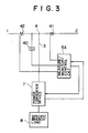
- Fig. 3 shows a thyrister converter system with a means for suppressing higher harmonics according to this invention.
- a branch 3 is connected to an intermediate point 4 between the feeder supply side 1 and a load side 2.
- the outputs of the instrument transformers 40, 41, and 42 which detect the voltage at the node point, the load current at the side of the user, and the current at the power system side, respectivly, are introduced to the measurement/monitor/control circuit 5A, which measures and monitors the higher harmonics as described hereinbelow.
- a semiconductor power supply device 7, e.g., a thyrister bridge type converter circuit connected to the node 4 supplies a power to the branch load 8 in response to the output of the control circuit 5A.
- the measurement/monitor/control circuit 5A determines, on the basis of the outputs of the potential transformer 40 and the current transformers 41 and 42, etc., the voltage and the currents containing higher harmonics which are present in the power; on the basis of these determinations, the control circuit 5A controls the thyrister converter circuit 7 when necessary. As a result of this, the electrical input applied to the load 8 becomes somewhat different from that which should have been introduced thereto under no control. However, when the power system under consideration is viewed as a whole, the input conditions which the load connected thereto requires is satisfied, such that the higher harmonics contents can substantially be reduced without affecting the intrinsic operations of the load, as described in detail hereinbelow.
- Fig. 4 shows an example of the instrumentation of the control circuit 5A, together with details of other circuit elements.
- the control circuit 5A comprises inupt terminals 50-1 through 50-5.
- To the input terminals 50-1 through 50-3 are introduced the outputs of the transformers 40 through 42, respectively; on the other hand, to the input terminals 50-4 and 50-5 are given the outputs of a potential transformer 80 and a current transformer 81 respectively, as described hereinbelow.
- Converters 51-1 through 51-5 coupled to the input terminals 50-1 through 50-5, respectively, convert the voltages and the currents inputted to the respective input terminals to corresponding voltages of appropriate magnitudes.
- the sample hold amplifiers 52-1 through 52-5 connected to the converters 51-1 through 51-5, respectively, hold and store therein at proper instance the respective outputs of the converters connected thereto.
- a multiplexer 53 connected to the sample hold amplifiers 52-1 through 52-5 switches over(i.e., successively changes over) the outputs of the analog outputs of the sample and hold amplifiers, so as to supply the multiplexed analog outputs of the sample hold amplifiers to the A/D converter 54.
- the A/D converter 54 converts into a corresponding digital output the multiplexed analog sample voltages received from the multiplexer 53.
- a microprocessor 55 receives this digital output from the A/D converter 54 and performs predetermined logical and arithmetic operations thereon.
- the ROM 56 stores, for example, the trigonometric functions table in a tabular data form, so as to offer an auxiliary memory means for the numerical operations of the microprocessor 55.
- An output interface 57 consisting of a so-called level-converter circuit, is provided for yielding via the output terminal 58 the results of the judgements of the microprocessor 55 obtained from the operations thereof.
- the above component parts 50 through 58 are comprised in the measurement/monitor/ control circuit 5A.
- the thyrister bridge type converter circuit 7 comprises: a power converter circuit unit 70 utilizing thyristers or transistors as switching elements, and a control circuit unit 71.
- the control unit 71 having an input connected to the outut terminal 58 of the control circuit 5A, generates, in response to the result of the judgement of the micorprocessor 55 received via the interface 57 and output terminal 58 of the control 5A, a wave-shaped pulse signal to control the converter firing circuit unit 70.
- the control circuit unit 71 comprises another input coupled to a feedback from the load 8, etc.
- the potential transformer 80 and the currrent transformer 81 measure the voltage and the current supplied to the branch load 8, respectively. The outputs of these transformers 80 and 81 are given to the control circuit 5A via the input terminals 50-4 and 50-5, respectively.
- Fig. 5 is the flow chart showing the operations of the embodiment according to this invention as shown in Figs. 3 and 4, wherein Fig. 5(A) and Fig. 5(B) show the first and the second half, respectively.
- step S1 the voltage Ed and the current Id at the output side of the thyrister converter circuit 7 are measured.
- step S2 from the instantaneous values of the voltages and currents which are taken into the microprocessor 55 of the control circuit 5A, the values thereof of the power supply side 1, the load side 2, and the branch load side 8 are measured, and the control delay angle and the overlap angle u are determined.
- step S3 utilizing the voltage Ed and current Id as determined at step S1, and the delay angle ⁇ and the overlap angle u as determined at step S2, the reactance Xs of the power supply side 1 is estimated by means of the equation (2) above.
- HHF high harmonic frequency components
- step S6 the HHF or higher harmonics contents are discriminated as in the step S4.
- step S7 it is discriminated whether the higher harmonics contents as determined above are within predetermined allowable range.
- step S7 When the judgement at step S7 is acceptable, the voltage Ed and the current Id at the side of the load 8 are measured again at step S8; further, at the subsequent step S9, the time integral of the input variation to the load 8 is calculated. Furthermore, at step S10, it is discriminated whether or not the integral of the input variation to the load side as determined above is within a predetermined allowable limits. When the discrimination at step S10 is of no problem, the reactance Xs of the power source 1 is estimated again, thereby ending the series of operations.
- step S5 when the adjustment of the value of the delay angle ⁇ at step S5 is not appropriate, and hence the reductions of the higher harmonics contents to predetermined small levels could not be effected, the delay angle ⁇ should be readjusted.
- step S12 when it is determi at step S7 that the higher harmonics contents as ⁇ are not within the predetermined allowable range, the control proceeds to step S12 where it is judged whether the values of the delay angle ⁇ and the overlap angle u satisfying the above equation (3) which reduce the higher harmonics contents below the predetermined levels can be found or not. If the condition at step S12 is met, the sequence goes back to the step S2 as described above.
- step S12 when the condition at step S12 is not met, the procedure goes over to step S13 where the adjustment at the power input side 1 is effected.
- step S10 and S12 when the condition at step S10 and S12 are not met (i.e., when it is judged that the harmonics contents as determined are not within the allowable limits and besides the solution of delay angle ⁇ and angle of overlap u satisfying equation (3) can not be found), the procedure goes over to step S13 where the input adjustment at the power supply side 1 is effected.
- the values of the delay angle ⁇ and the overlap angle u satisfying the above equation (3) can be determined such that higher harmonics contents are kept under predetermined levels and such that the integral of the input variation to the load 8 is maintained within allowable limits.
- the input adjustments by means of external source adjustment device are effected at step S13.
- the philosophy of this invention is applicable with the modification of the control means when the above distortion can not be ignored.
Landscapes
- Engineering & Computer Science (AREA)
- Power Engineering (AREA)
- Supply And Distribution Of Alternating Current (AREA)
- Power Conversion In General (AREA)
- Inverter Devices (AREA)
- Rectifiers (AREA)
Applications Claiming Priority (2)
| Application Number | Priority Date | Filing Date | Title |
|---|---|---|---|
| JP239837/89 | 1989-09-18 | ||
| JP1239837A JP2690155B2 (ja) | 1989-09-18 | 1989-09-18 | 高調波抑制方式 |
Publications (3)
| Publication Number | Publication Date |
|---|---|
| EP0419217A2 true EP0419217A2 (fr) | 1991-03-27 |
| EP0419217A3 EP0419217A3 (en) | 1991-07-03 |
| EP0419217B1 EP0419217B1 (fr) | 1996-12-18 |
Family
ID=17050600
Family Applications (1)
| Application Number | Title | Priority Date | Filing Date |
|---|---|---|---|
| EP19900310210 Expired - Lifetime EP0419217B1 (fr) | 1989-09-18 | 1990-09-18 | Système convertisseur à thyristor avec suppression des harmoniques |
Country Status (4)
| Country | Link |
|---|---|
| EP (1) | EP0419217B1 (fr) |
| JP (1) | JP2690155B2 (fr) |
| CA (1) | CA2025505C (fr) |
| DE (1) | DE69029447T2 (fr) |
Cited By (1)
| Publication number | Priority date | Publication date | Assignee | Title |
|---|---|---|---|---|
| US6437995B2 (en) | 2000-02-18 | 2002-08-20 | Alstom | Control system adapted to control operation of an ac/dc converter |
Family Cites Families (3)
| Publication number | Priority date | Publication date | Assignee | Title |
|---|---|---|---|---|
| JPS5492165A (en) * | 1977-12-29 | 1979-07-21 | Fuji Electric Co Ltd | Controlling method for thyristor converter |
| JPS6198390U (fr) * | 1984-11-30 | 1986-06-24 | ||
| JPH0834669B2 (ja) * | 1986-06-26 | 1996-03-29 | 三菱電機株式会社 | 高調波抑制装置 |
-
1989
- 1989-09-18 JP JP1239837A patent/JP2690155B2/ja not_active Expired - Lifetime
-
1990
- 1990-09-17 CA CA 2025505 patent/CA2025505C/fr not_active Expired - Fee Related
- 1990-09-18 DE DE1990629447 patent/DE69029447T2/de not_active Expired - Fee Related
- 1990-09-18 EP EP19900310210 patent/EP0419217B1/fr not_active Expired - Lifetime
Cited By (1)
| Publication number | Priority date | Publication date | Assignee | Title |
|---|---|---|---|---|
| US6437995B2 (en) | 2000-02-18 | 2002-08-20 | Alstom | Control system adapted to control operation of an ac/dc converter |
Also Published As
| Publication number | Publication date |
|---|---|
| JP2690155B2 (ja) | 1997-12-10 |
| JPH03103032A (ja) | 1991-04-30 |
| CA2025505C (fr) | 1995-09-26 |
| EP0419217B1 (fr) | 1996-12-18 |
| EP0419217A3 (en) | 1991-07-03 |
| DE69029447D1 (de) | 1997-01-30 |
| CA2025505A1 (fr) | 1991-03-19 |
| DE69029447T2 (de) | 1997-06-26 |
Similar Documents
| Publication | Publication Date | Title |
|---|---|---|
| RU2484572C2 (ru) | Системы и способы управления работой ипб | |
| US5903449A (en) | Bi-directional power control system for voltage converter | |
| US7031176B2 (en) | Inverter | |
| US8625307B2 (en) | DC to AC power converting apparatus | |
| US5532918A (en) | High power factor switched DC power supply | |
| JP3221828B2 (ja) | 電力変換方法及び電力変換装置 | |
| EP0475709B1 (fr) | Dispositif de contrôle d'un onduleur capable de supprimer la composante continue de magnétisation du transformateur triphasé | |
| US4930064A (en) | Phase stabilized high frequency link power converter apparatus having a wide phase controllable range | |
| EP0802618B1 (fr) | Dispositif de régulation d'un convertisseur à plusieurs niveaux | |
| WO1991011841A1 (fr) | Cycloconvertisseur | |
| JP4872090B2 (ja) | 電圧調整装置 | |
| US7778053B2 (en) | Power system having a voltage regulator with a notch filter | |
| EP0126180A2 (fr) | Circuit de réduction des harmoniques ou pulsations dans des systèmes de redressement polyphasé multiplexe ou dans des convertisseurs, respectivement pourvus de bobine d'absorption | |
| US5347441A (en) | Thyristor converter system with higher harmonics suppression | |
| EP0419217B1 (fr) | Système convertisseur à thyristor avec suppression des harmoniques | |
| US4509108A (en) | Three phase a.c. to d.c. voltage converter with improved power line harmonic current reduction | |
| EP0085249A1 (fr) | Procédé et appareil de conversion de puissance électrique | |
| JPS5935534A (ja) | 電力変換装置 | |
| JPH0432621B2 (fr) | ||
| US20250274054A1 (en) | Power conversion device | |
| RU2096888C1 (ru) | Способ регулирования реактивной мощности и устройство для его осуществления | |
| JP2644590B2 (ja) | 電圧変動補償装置 | |
| JPH02276475A (ja) | 電力変換装置 | |
| SU987783A1 (ru) | Способ управлени преобразователем частоты | |
| UA151183U (uk) | Трифазний дворівневий силовий активний фільтр для трифазної чотирипровідної електричної мережі |
Legal Events
| Date | Code | Title | Description |
|---|---|---|---|
| PUAI | Public reference made under article 153(3) epc to a published international application that has entered the european phase |
Free format text: ORIGINAL CODE: 0009012 |
|
| 17P | Request for examination filed |
Effective date: 19901228 |
|
| AK | Designated contracting states |
Kind code of ref document: A2 Designated state(s): CH DE GB LI SE |
|
| PUAL | Search report despatched |
Free format text: ORIGINAL CODE: 0009013 |
|
| AK | Designated contracting states |
Kind code of ref document: A3 Designated state(s): CH DE GB LI SE |
|
| 17Q | First examination report despatched |
Effective date: 19930816 |
|
| GRAG | Despatch of communication of intention to grant |
Free format text: ORIGINAL CODE: EPIDOS AGRA |
|
| GRAH | Despatch of communication of intention to grant a patent |
Free format text: ORIGINAL CODE: EPIDOS IGRA |
|
| GRAH | Despatch of communication of intention to grant a patent |
Free format text: ORIGINAL CODE: EPIDOS IGRA |
|
| GRAA | (expected) grant |
Free format text: ORIGINAL CODE: 0009210 |
|
| AK | Designated contracting states |
Kind code of ref document: B1 Designated state(s): CH DE GB LI SE |
|
| REG | Reference to a national code |
Ref country code: CH Ref legal event code: NV Representative=s name: WILLIAM BLANC & CIE CONSEILS EN PROPRIETE INDUSTRI |
|
| REF | Corresponds to: |
Ref document number: 69029447 Country of ref document: DE Date of ref document: 19970130 |
|
| REG | Reference to a national code |
Ref country code: GB Ref legal event code: 727 |
|
| REG | Reference to a national code |
Ref country code: GB Ref legal event code: 727A |
|
| REG | Reference to a national code |
Ref country code: GB Ref legal event code: 727B |
|
| REG | Reference to a national code |
Ref country code: GB Ref legal event code: SP |
|
| PLBE | No opposition filed within time limit |
Free format text: ORIGINAL CODE: 0009261 |
|
| STAA | Information on the status of an ep patent application or granted ep patent |
Free format text: STATUS: NO OPPOSITION FILED WITHIN TIME LIMIT |
|
| 26N | No opposition filed | ||
| REG | Reference to a national code |
Ref country code: GB Ref legal event code: IF02 |
|
| PGFP | Annual fee paid to national office [announced via postgrant information from national office to epo] |
Ref country code: SE Payment date: 20020904 Year of fee payment: 13 |
|
| PGFP | Annual fee paid to national office [announced via postgrant information from national office to epo] |
Ref country code: GB Payment date: 20020918 Year of fee payment: 13 |
|
| PGFP | Annual fee paid to national office [announced via postgrant information from national office to epo] |
Ref country code: DE Payment date: 20020925 Year of fee payment: 13 |
|
| PGFP | Annual fee paid to national office [announced via postgrant information from national office to epo] |
Ref country code: CH Payment date: 20021001 Year of fee payment: 13 |
|
| PG25 | Lapsed in a contracting state [announced via postgrant information from national office to epo] |
Ref country code: GB Free format text: LAPSE BECAUSE OF NON-PAYMENT OF DUE FEES Effective date: 20030918 |
|
| PG25 | Lapsed in a contracting state [announced via postgrant information from national office to epo] |
Ref country code: SE Free format text: LAPSE BECAUSE OF NON-PAYMENT OF DUE FEES Effective date: 20030919 |
|
| PG25 | Lapsed in a contracting state [announced via postgrant information from national office to epo] |
Ref country code: LI Free format text: LAPSE BECAUSE OF NON-PAYMENT OF DUE FEES Effective date: 20030930 Ref country code: CH Free format text: LAPSE BECAUSE OF NON-PAYMENT OF DUE FEES Effective date: 20030930 |
|
| PG25 | Lapsed in a contracting state [announced via postgrant information from national office to epo] |
Ref country code: DE Free format text: LAPSE BECAUSE OF NON-PAYMENT OF DUE FEES Effective date: 20040401 |
|
| EUG | Se: european patent has lapsed | ||
| GBPC | Gb: european patent ceased through non-payment of renewal fee |
Effective date: 20030918 |
|
| REG | Reference to a national code |
Ref country code: CH Ref legal event code: PL |