EP0419693A1 - Procédé de passivation des défauts cristallins dans du silicium polycristallin - Google Patents
Procédé de passivation des défauts cristallins dans du silicium polycristallin Download PDFInfo
- Publication number
- EP0419693A1 EP0419693A1 EP89117694A EP89117694A EP0419693A1 EP 0419693 A1 EP0419693 A1 EP 0419693A1 EP 89117694 A EP89117694 A EP 89117694A EP 89117694 A EP89117694 A EP 89117694A EP 0419693 A1 EP0419693 A1 EP 0419693A1
- Authority
- EP
- European Patent Office
- Prior art keywords
- silicon material
- hydrogen
- crystal defects
- passivation
- polycrystalline
- Prior art date
- Legal status (The legal status is an assumption and is not a legal conclusion. Google has not performed a legal analysis and makes no representation as to the accuracy of the status listed.)
- Ceased
Links
Images
Classifications
-
- H—ELECTRICITY
- H10—SEMICONDUCTOR DEVICES; ELECTRIC SOLID-STATE DEVICES NOT OTHERWISE PROVIDED FOR
- H10P—GENERIC PROCESSES OR APPARATUS FOR THE MANUFACTURE OR TREATMENT OF DEVICES COVERED BY CLASS H10
- H10P95/00—Generic processes or apparatus for manufacture or treatments not covered by the other groups of this subclass
- H10P95/94—Hydrogenation or deuterisation, e.g. using atomic hydrogen from a plasma
-
- Y—GENERAL TAGGING OF NEW TECHNOLOGICAL DEVELOPMENTS; GENERAL TAGGING OF CROSS-SECTIONAL TECHNOLOGIES SPANNING OVER SEVERAL SECTIONS OF THE IPC; TECHNICAL SUBJECTS COVERED BY FORMER USPC CROSS-REFERENCE ART COLLECTIONS [XRACs] AND DIGESTS
- Y10—TECHNICAL SUBJECTS COVERED BY FORMER USPC
- Y10S—TECHNICAL SUBJECTS COVERED BY FORMER USPC CROSS-REFERENCE ART COLLECTIONS [XRACs] AND DIGESTS
- Y10S136/00—Batteries: thermoelectric and photoelectric
- Y10S136/29—Testing, calibrating, treating, e.g. aging
-
- Y—GENERAL TAGGING OF NEW TECHNOLOGICAL DEVELOPMENTS; GENERAL TAGGING OF CROSS-SECTIONAL TECHNOLOGIES SPANNING OVER SEVERAL SECTIONS OF THE IPC; TECHNICAL SUBJECTS COVERED BY FORMER USPC CROSS-REFERENCE ART COLLECTIONS [XRACs] AND DIGESTS
- Y10—TECHNICAL SUBJECTS COVERED BY FORMER USPC
- Y10S—TECHNICAL SUBJECTS COVERED BY FORMER USPC CROSS-REFERENCE ART COLLECTIONS [XRACs] AND DIGESTS
- Y10S148/00—Metal treatment
- Y10S148/128—Proton bombardment of silicon
Definitions
- the invention relates to a method for passivation of crystal defects in polycrystalline silicon material according to the preamble of claim 1.
- Polycrystalline silicon wafers or silicon layers or silicon material of any shape usually have crystal defects such as. B. point defects or line defects, dislocations or grain boundaries. These crystal defects are reflected in a reduced quality of the electronic components made from such silicon material. Solar cells or photodiodes made of such silicon materials have reduced photocurrent sensitivities and open circuit voltages due to increased recombination currents. Basically, when using such silicon materials, unfavorable diode properties result.
- the present invention also relates to the passivation of amorphous silicon material.
- Amorphous silicon material is also used for solar cells, photodiodes and for electrographic recording materials.
- the present invention is based on the object of specifying a method of the type mentioned at the outset which in a simple manner enables favorable diode properties and / or favorable passivation properties in the case of amorphous or polycrystalline silicon material.
- the invention enables an improvement of solar cell parameters in a simple manner.
- the invention enables improved production of electronic components from polycrystalline or amorphous silicon material in a simple manner.
- the invention is explained in more detail below with reference to the drawing.
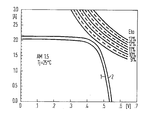
- the figure shows I-U characteristics of polycrystalline solar cells without an anti-reflective layer before and after a temperature treatment for the passivation of crystal defects.
- the passivation of grain boundaries and inner grain defects in silicon material can be done by saturating these crystal perturbations with hydrogen atoms. To do this, the two process steps of generating atomic hydrogen and transporting it to the crystal perturbation must be accomplished. A diffusion process is most suitable for the non-destructive transport of the hydrogen atoms generated to the crystal perturbation.
- Hydrogen atoms are generated by reducing hydrogen-oxygen compounds, e.g. B. water, on the silicon surface.
- hydrogen-containing compounds are suitable, whose dissociation energies at a certain temperature are smaller than the binding energy of silicon dioxide (SiO2).
- SiO2 silicon dioxide
- polycrystalline silicon wafers were subjected to a temperature treatment in a water-containing atmosphere.
- the temperature range is preferably between approximately 250 ° C. and 500 ° C. Improvements in the short-circuit current, in the open circuit voltage and in the fill factor were found on solar cells made of silicon material treated in this way, similar to the use of common passivation processes.
- the figure shows current-voltage characteristics of polycrystalline solar cells before and after such a treatment in a water-containing atmosphere.
- Curve 1 shows the current-voltage characteristic of polycrystalline solar cells without an anti-reflective layer before the temperature treatment.
- Curve 2 shows the current-voltage characteristic of the same polycrystalline solar cell without an anti-reflective layer after a temperature treatment of 330 ° C. in a water-containing atmosphere for the passivation of crystal defects.
- a comparison between curves 1 and 2 in the figure clearly shows the improvement in the solar cell parameters "short-circuit current" and "open circuit voltage".
- a method according to the invention can be carried out in a normal atmosphere.
- a method according to the invention can also be carried out at elevated pressure in order to achieve a higher passivation effect.
Landscapes
- Photovoltaic Devices (AREA)
- Light Receiving Elements (AREA)
Priority Applications (3)
| Application Number | Priority Date | Filing Date | Title |
|---|---|---|---|
| EP89117694A EP0419693A1 (fr) | 1989-09-25 | 1989-09-25 | Procédé de passivation des défauts cristallins dans du silicium polycristallin |
| US07/585,522 US5169791A (en) | 1989-09-25 | 1990-09-20 | Method for the passivation of crystal defects in polycrystalline silicon material |
| JP2253986A JPH03120725A (ja) | 1989-09-25 | 1990-09-21 | 多結晶又は非晶質シリコン材中の結晶欠陥の不動態化法 |
Applications Claiming Priority (1)
| Application Number | Priority Date | Filing Date | Title |
|---|---|---|---|
| EP89117694A EP0419693A1 (fr) | 1989-09-25 | 1989-09-25 | Procédé de passivation des défauts cristallins dans du silicium polycristallin |
Publications (1)
| Publication Number | Publication Date |
|---|---|
| EP0419693A1 true EP0419693A1 (fr) | 1991-04-03 |
Family
ID=8201925
Family Applications (1)
| Application Number | Title | Priority Date | Filing Date |
|---|---|---|---|
| EP89117694A Ceased EP0419693A1 (fr) | 1989-09-25 | 1989-09-25 | Procédé de passivation des défauts cristallins dans du silicium polycristallin |
Country Status (3)
| Country | Link |
|---|---|
| US (1) | US5169791A (fr) |
| EP (1) | EP0419693A1 (fr) |
| JP (1) | JPH03120725A (fr) |
Cited By (2)
| Publication number | Priority date | Publication date | Assignee | Title |
|---|---|---|---|---|
| DE102009008371A1 (de) * | 2009-02-11 | 2010-08-12 | Schott Solar Ag | Integraler Prozeß von Waferherstellung bis Modulfertigung zur Herstellung von Wafern, Solarzellen und Solarmodulen |
| DE102010053214A1 (de) | 2010-12-03 | 2012-06-06 | Evonik Degussa Gmbh | Verfahren zur Wasserstoffpassivierung von Halbleiterschichten |
Families Citing this family (11)
| Publication number | Priority date | Publication date | Assignee | Title |
|---|---|---|---|---|
| TW226478B (en) * | 1992-12-04 | 1994-07-11 | Semiconductor Energy Res Co Ltd | Semiconductor device and method for manufacturing the same |
| JPH07153769A (ja) * | 1993-11-30 | 1995-06-16 | Hitachi Ltd | 半導体集積回路装置の製造方法および製造装置 |
| US5426061A (en) * | 1994-09-06 | 1995-06-20 | Midwest Research Institute | Impurity gettering in semiconductors |
| US5489553A (en) * | 1995-05-25 | 1996-02-06 | Industrial Technology Research Institute | HF vapor surface treatment for the 03 teos gap filling deposition |
| JP4041182B2 (ja) * | 1997-01-27 | 2008-01-30 | Sumco Techxiv株式会社 | 熱処理用シリコンウェーハ及びその製造方法 |
| US6319843B1 (en) | 1999-06-08 | 2001-11-20 | Advanced Micro Devices | Nitride surface passivation for acid catalyzed chemically amplified resist processing |
| JP4413841B2 (ja) * | 2005-10-03 | 2010-02-10 | 株式会社東芝 | 半導体記憶装置及びその製造方法 |
| US20090101202A1 (en) | 2007-10-17 | 2009-04-23 | Industrial Technology Research Institute | Method of fast hydrogen passivation to solar cells made of crystalline silicon |
| CN102244137A (zh) * | 2010-05-14 | 2011-11-16 | 北京北方微电子基地设备工艺研究中心有限责任公司 | 太阳能电池及其制造方法 |
| DE102010049587A1 (de) | 2010-10-26 | 2012-04-26 | Evonik Degussa Gmbh | Verfahren zur elektrochemischen Wasserstoffpassivierung von Halbleiterschichten |
| TW201742259A (zh) * | 2016-05-16 | 2017-12-01 | 昱晶能源科技股份有限公司 | 氫化太陽能電池之方法及其裝置 |
Citations (2)
| Publication number | Priority date | Publication date | Assignee | Title |
|---|---|---|---|---|
| US4113514A (en) * | 1978-01-16 | 1978-09-12 | Rca Corporation | Method of passivating a semiconductor device by treatment with atomic hydrogen |
| EP0264762A1 (fr) * | 1986-10-24 | 1988-04-27 | Siemens Aktiengesellschaft | Méthode pour passiver les défauts cristallins dans un plasma d'hydrogène |
Family Cites Families (1)
| Publication number | Priority date | Publication date | Assignee | Title |
|---|---|---|---|---|
| JPS5845176B2 (ja) * | 1979-03-05 | 1983-10-07 | 日本電信電話株式会社 | 3↓−5族化合物半導体のプラズマ陽極酸化法 |
-
1989
- 1989-09-25 EP EP89117694A patent/EP0419693A1/fr not_active Ceased
-
1990
- 1990-09-20 US US07/585,522 patent/US5169791A/en not_active Expired - Fee Related
- 1990-09-21 JP JP2253986A patent/JPH03120725A/ja active Pending
Patent Citations (2)
| Publication number | Priority date | Publication date | Assignee | Title |
|---|---|---|---|---|
| US4113514A (en) * | 1978-01-16 | 1978-09-12 | Rca Corporation | Method of passivating a semiconductor device by treatment with atomic hydrogen |
| EP0264762A1 (fr) * | 1986-10-24 | 1988-04-27 | Siemens Aktiengesellschaft | Méthode pour passiver les défauts cristallins dans un plasma d'hydrogène |
Non-Patent Citations (3)
| Title |
|---|
| EXTENDED ABSTRACTS, Band 86-1, Nr. 1, Mai 1986, Seite 460, Zusammenfassung Nr. 315, Princeton, New Jersey, US; L. AMMOR et al.: "Improvement of polycrystalline silicon wafers and solar cells by annealing in hydrogen gas flow" * |
| IBM TECHNICAL DISCLOSURE BULLETIN, Band 25, Nr. 3B, August 1982, Seiten 1683-1684, New York, US; J.M. AITKEN et al.: "Wet forming gas anneal to remove radiation damage from polysilicon gate MOSFETS" * |
| INTERNATIONAL JOURNAL OF ELECTRONICS, Band 58, Nr. 5, 1985, Seiten 769-774, Taylor and Francis Ltd, London, GB; A. AGARWAL et al.: "Passivation of defects in polycrystalline silicon solar cells by molecular hydrogen annealing" * |
Cited By (3)
| Publication number | Priority date | Publication date | Assignee | Title |
|---|---|---|---|---|
| DE102009008371A1 (de) * | 2009-02-11 | 2010-08-12 | Schott Solar Ag | Integraler Prozeß von Waferherstellung bis Modulfertigung zur Herstellung von Wafern, Solarzellen und Solarmodulen |
| DE102010053214A1 (de) | 2010-12-03 | 2012-06-06 | Evonik Degussa Gmbh | Verfahren zur Wasserstoffpassivierung von Halbleiterschichten |
| WO2012072403A1 (fr) | 2010-12-03 | 2012-06-07 | Evonik Degussa Gmbh | Procédé de passivation à l'hydrogène de couches de semi-conducteurs |
Also Published As
| Publication number | Publication date |
|---|---|
| JPH03120725A (ja) | 1991-05-22 |
| US5169791A (en) | 1992-12-08 |
Similar Documents
| Publication | Publication Date | Title |
|---|---|---|
| DE69411078T2 (de) | Isotopenbatterien | |
| EP0419693A1 (fr) | Procédé de passivation des défauts cristallins dans du silicium polycristallin | |
| DE19634617B4 (de) | Verfahren zur Herstellung einer Siliziumsolarzelle mit verringerter Rekombination nahe der Solarzellenoberfläche | |
| DE3650287T2 (de) | Halbleiter-Photodetektor mit einem zweistufigen Verunreinigungsprofil. | |
| DE60033252T2 (de) | Mehrschichtige halbleiter-struktur mit phosphid-passiviertem germanium-substrat | |
| DE3742110C2 (de) | Verfahren zur Bildung funktioneller aufgedampfter Filme durch ein chemisches Mikrowellen-Plasma-Aufdampfverfahren | |
| DE102004013627A1 (de) | Solarzelle mit mehreren Übergängen sowie Stromanpassungsverfahren | |
| DE2752439A1 (de) | Verfahren zur herstellung von silicium-halbleiteranordnungen unter einsatz einer ionenimplantation und zugehoerige halbleiteranordnung | |
| DE112019006396T5 (de) | Freistehendes polykristallines diamantsubstrat und verfahren zur herstellung desselben | |
| EP0182377A2 (fr) | Procédé de fabrication d'un condensateur à couche mince | |
| DE3416954A1 (de) | Ternaere iii-v-multicolor-solarzellen mit einer quaternaeren fensterschicht und einer quaternaeren uebergangsschicht | |
| DE2259829A1 (de) | Verfahren zur behandlung von galliumhaltigen verbindungshalbleitern | |
| DE3310545C2 (de) | Nicht-massenanalysiertes Ionenimplantationsverfahren | |
| DE112018003666T5 (de) | Verfahren zur herstellung eines halbleiterbauelements und halbleiterbauelement | |
| DE102010053214A1 (de) | Verfahren zur Wasserstoffpassivierung von Halbleiterschichten | |
| DE2908146A1 (de) | Amorpher halbleiter und verfahren zu seiner herstellung | |
| EP1601813B1 (fr) | Procede de depot de silicium | |
| DE2453134B2 (de) | Planardiffusionsverfahren | |
| DE3234678C2 (fr) | ||
| DE3340583A1 (de) | Verfahren zum herstellen einer isolierschicht und halbleiterbauelement | |
| DE69023582T2 (de) | Verfahren zur Herstellung eines Halbleiterelementes mittels Ionen-Implantation. | |
| DE69222074T2 (de) | Verfahren zur Herstellung eines neutronenumwandlungsdotierten Czochralski-Silizium-Einkristalls | |
| EP0264762B1 (fr) | Méthode pour passiver les défauts cristallins dans un plasma d'hydrogène | |
| EP2012367B1 (fr) | Cellule solaire multiple | |
| DE3434552C2 (fr) |
Legal Events
| Date | Code | Title | Description |
|---|---|---|---|
| PUAI | Public reference made under article 153(3) epc to a published international application that has entered the european phase |
Free format text: ORIGINAL CODE: 0009012 |
|
| 17P | Request for examination filed |
Effective date: 19901220 |
|
| AK | Designated contracting states |
Kind code of ref document: A1 Designated state(s): AT BE CH DE ES FR GB GR IT LI LU NL SE |
|
| RBV | Designated contracting states (corrected) |
Designated state(s): DE FR GB IT |
|
| 17Q | First examination report despatched |
Effective date: 19921008 |
|
| STAA | Information on the status of an ep patent application or granted ep patent |
Free format text: STATUS: THE APPLICATION HAS BEEN REFUSED |
|
| 18R | Application refused |
Effective date: 19960816 |