EP0419959B1 - Circuit pour contrÔler le respet de débits préétablis lors de la transmission de cellules de données - Google Patents
Circuit pour contrÔler le respet de débits préétablis lors de la transmission de cellules de données Download PDFInfo
- Publication number
- EP0419959B1 EP0419959B1 EP90117685A EP90117685A EP0419959B1 EP 0419959 B1 EP0419959 B1 EP 0419959B1 EP 90117685 A EP90117685 A EP 90117685A EP 90117685 A EP90117685 A EP 90117685A EP 0419959 B1 EP0419959 B1 EP 0419959B1
- Authority
- EP
- European Patent Office
- Prior art keywords
- bit rate
- counter reading
- counting
- transmission
- message
- Prior art date
- Legal status (The legal status is an assumption and is not a legal conclusion. Google has not performed a legal analysis and makes no representation as to the accuracy of the status listed.)
- Expired - Lifetime
Links
Images
Classifications
-
- H—ELECTRICITY
- H04—ELECTRIC COMMUNICATION TECHNIQUE
- H04L—TRANSMISSION OF DIGITAL INFORMATION, e.g. TELEGRAPHIC COMMUNICATION
- H04L12/00—Data switching networks
- H04L12/54—Store-and-forward switching systems
- H04L12/56—Packet switching systems
- H04L12/5601—Transfer mode dependent, e.g. ATM
- H04L12/5602—Bandwidth control in ATM Networks, e.g. leaky bucket
-
- H—ELECTRICITY
- H04—ELECTRIC COMMUNICATION TECHNIQUE
- H04L—TRANSMISSION OF DIGITAL INFORMATION, e.g. TELEGRAPHIC COMMUNICATION
- H04L12/00—Data switching networks
- H04L12/54—Store-and-forward switching systems
- H04L12/56—Packet switching systems
- H04L12/5601—Transfer mode dependent, e.g. ATM
- H04L2012/5629—Admission control
- H04L2012/5631—Resource management and allocation
- H04L2012/5636—Monitoring or policing, e.g. compliance with allocated rate, corrective actions
- H04L2012/5637—Leaky Buckets
Definitions
- the invention relates to a circuit arrangement according to the preamble of patent claim 1.
- each subscriber device connected to it is assigned two upward counters instead of an up-down counter, a first counter counting the cells sent by the respective subscriber device and the remaining counter determining the connection time accumulated during the existing connection.
- the two counters are connected to a device which uses the ratio of the meter readings to check whether the maximum bit rate determined by the respective subscriber device is being observed.
- EP 0 293 315 A1 discloses a circuit arrangement for controlling the transmission of data packets in a system operating according to the ATM principle.
- This system has a plurality of virtual connections individually assigned counting devices which are controlled by a central control device.
- Each of these counting devices is formed from an up / down counter, the current count of which is incremented by the value “1” each time a data packet occurs in the virtual connection assigned to the respective counting device.
- the current counter reading is decremented in accordance with the maximum transmission bit rate required for the respective virtual connection and the time difference between the occurrence of the data packet just present and the immediately preceding data packet of the same virtual connection.
- the up / down counters therefore work according to the so-called “leaky bucket" principle. If the instantaneous counter reading of an up / down counter resulting from the incrementing and decrementing exceeds a defined threshold value, then a signal is emitted by the respective counter, which indicates that the maximum transmission bit rate has been exceeded.
- the invention has the advantage that, for the counting operation of the unidirectional counting devices, a bit rate value corresponding to the required maximum transmission bit rate only has to be recorded in the course of establishing a virtual connection, in order to determine the current counter reading of the respective one when a message cell of this virtual connection occurs
- Counter device is to be changed, by means of the connection-specific counting devices, the virtual connections running over any feeder lines connected to an ATM switching system can be checked individually in terms of compliance with fixed transmission bit rates in a simple manner. For example, a connection-specific check of defined transmission bit rates for feeder lines is possible, which are shared by a multiplicity of subscriber devices in multiplex operation. Such a connection-specific check can also be carried out in the event that subscriber devices are simultaneously involved in several virtual connections.
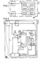
- FIG. 1 schematically shows an ATM switching system BVA, to which a plurality of feeder lines E1 to En and a plurality of customer lines A1 to An are connected. Of these, only the feeder lines E1 and En and the customer lines A1 to An are indicated in FIG.
- Message cells are each transmitted on the feeder lines and customer lines in the course of virtual connections using an asynchronous transfer method ("Asynchronous Transfer Mode").
- the message cells may be cells of fixed length, each of which catches via a cell header with a virtual channel number that designates the respective virtual connection and an information part.
- the actual message signals are transmitted in the information section. Under news signals Data and text signals as well as voice and image signals should be understood in digital form. Moreover, it should already be pointed out here that the present invention can also be used when message signals are transmitted in the course of virtual connections in cells of variable length.
- a treatment device BHE is assigned to each of the feeder lines E1 to En.
- Such a treatment device receives the message cells transmitted in the course of virtual connections via the assigned feeder line and, before forwarding them to a coupling arrangement KA of the ATM switching system, carries out a connection-specific check of compliance with the requirements for the respective one transmission rate set by virtual connection.
- a coupling arrangement KA a multi-stage structure with a plurality of mutually connected switching multiples KV is given in FIG. 1 merely as an example.
- any one- or multi-stage coupling arrangements can also be used. Since the structure and mode of operation of such coupling arrangements for the forwarding of message cells to customer lines designated A1 to An in FIG. 1 is known, this will not be discussed in more detail below.
- FIG. 2 shows a possible construction of the previously mentioned treatment devices BHE constructed in the same way. Only those circuit parts are specified which are necessary for understanding the present invention.
- An interface device S is connected to the respective feeder line, which is denoted by E in FIG. 2, which on the one hand recognizes the beginning of message cells transmitted in serial form and on the other hand bits that occur in message cells to form bit groups with a fixed number of bits, for example 8 Bits, summarized and provides the individual bit groups (octets) in parallel via a line system.
- This interface device is followed by a register Reg1 as a delay device and a decoder DEC.
- This register Reg1 is run through by all the message cells to be forwarded to the switching arrangement KA already mentioned. The delay time is determined in such a way that the circuit arrangement described below can be used to check whether the transmission bit rate specified for the respective virtual connection has been met before the message cell just picked up is forwarded to the coupling arrangement KA.
- the cell header of a message cell included in the register Reg1 is additionally fed to the just mentioned decoder DEC which, by decoding the virtual channel number contained in this cell header, provides address signals which are fed to a bit rate memory BSP via first inputs of a multiplexer M.
- the bit rate memory BSP has a separate memory area for each of the virtual connections possible on the associated feeder line E.
- the individual memory areas can be individually controlled in accordance with the virtual channel numbers contained in message cells and decoded by the aforementioned decoder DEC. For example, if virtual connections designated "0" to "n-1" can run through the relevant feeder line, then, as indicated in FIG. 2, memory areas designated “0" to "n-1” are assigned to them. These are part of a counting device individually assigned to the respective virtual connection.
- the individual memory areas serve on the one hand for storing an instantaneous counter reading of the respective counting device, which is still to be explained, as well as an individually definable bit rate value, which is also yet to be explained.
- This storage takes place under the control of a control device designated ST in FIG. 2, which on the one hand has line systems with data inputs and data outputs of the bit rate memory BSP and, on the other hand, is connected to second inputs of the multiplexer M already mentioned and to the interface device S via a control line SL.
- the instantaneous counter readings and bit rate values stored for the virtual connections are designated by BRO to BRn-1 or ZSTO to ZSTn-1 in FIG. 2, according to their affiliation to the individual virtual connections.
- all of the counting devices assigned to a feeder line are associated with a common adding device which is available to the individual counting devices in multiplex mode.
- This adder has two registers designated Reg2 and Reg3 and an adder ADD. Load inputs of these registers are connected via a line system to data outputs of the bit rate memory BSP.
- the registers Reg2 and Reg3 are connected to inputs of the adder ADD. This has sum signal outputs connected to data inputs of the register Reg3 and an overflow output connected to a separate register space of the register Reg3.
- the register Reg3 is also connected to the control device ST.
- individually defined bit rate values are entered in the memory areas of the bit rate memory BSP assigned to the individual virtual connections.
- the determination takes place in the course of the establishment of the respective virtual connection by the control device ST, according to the stipulations a transmission bit rate specified by the subscriber device (calling subscriber device) wishing to establish the connection.
- the control device ST can assign a normalized bit rate value, for example the bit rate value "1", to a maximum transmission bit rate that can be specified.
- the assigned bit rate value is a multiple of the normalized bit rate value that corresponds to the ratio of the maximum transmission bit rate that can be specified to the current transmission bit rate.
- bit rate value is fixed at "2".
- the respective bit rate value is entered in the course of a write cycle from the control device ST by appropriate addressing via the multiplexer M into the memory area of the bit rate memory BSP that is suitable for the respective virtual connection for the entire connection duration.
- control device ST also controls all the memory areas of the bit rate memory BSP one after the other by address signals continuously provided via the multiplexer M for querying the instantaneous counter reading stored therein in each case. After the query has been carried out, the current meter reading is then converted into a defined initial meter reading.
- the initial counter reading may be set to "0", for example.
- a feeder cell now appears on the feeder line labeled E in FIG. 2, this is fed from the interface device S to the register Reg1 after an octet-wise conversion.
- the occurrence of the message cell is also controlled by the control device ST by means of the above-mentioned Control line SL transmitted signal signal displayed.
- the decoder DEC takes over from the interface device S the cell header contained in the message cell just occurring.
- the control device ST controls a read cycle in the bit rate memory BSP in accordance with the address signals provided by the decoder DEC via the multiplexer M.
- this bit rate memory provides the data stored in the memory area just addressed at its data outputs.
- these are a bit rate value defined for the respective virtual connection and a current counter reading.
- This current counter reading which may be the initial counter reading "0"
- the bit rate value just provided by the bit rate memory is fed to the register Reg2.
- the adder ADD connected to these registers then adds the bit rate value to the current counter reading, i.e. in the present case to the initial count "0".
- the resulting changed current meter reading is then entered in register Reg3, overwriting the initial meter reading previously recorded via load inputs.
- a write cycle then takes place in the bit rate memory BSP under the control of the control device ST.
- the current counter reading now stored in the register Reg3 is entered in the memory area addressed by the decoder DEC via the multiplexer M while overwriting the current counter reading previously stored therein. This completes the detection of the message cell that has just been added to the treatment unit BHE shown in FIG.
- the adder ADD is otherwise designed in such a way that, when a new instantaneous counter reading is formed, it indicates that a defined limit value has been exceeded by an overflow signal in the form of an overflow bit via the above-mentioned overflow output.
- This overflow bit is first transferred to the separate register space of register Reg3 already mentioned above and then transferred to the bit rate memory BSP as part of the current counter reading provided by the adder ADD.
- the limit value just mentioned is determined in accordance with the above-described bit rate values and the duration of a control cycle in such a way that it is always reached or exceeded by a current counter reading if, in the course of the respective virtual connection, message cells with a cell originally specified by a subscriber device Transmission bit rate higher transmission bit rate are transmitted.
- whether such a specified transmission bit rate is exceeded in this way is determined by the above-mentioned query of the current counter readings stored in the individual memory areas of the bit rate memory BSP.
- message signals are transmitted in fixed-length message cells in the course of virtual connections. If, on the other hand, such message cells have a variable length, the control cycles described above can also be modified in such a way that with each occurrence of a message cell the current counter reading is changed in the manner specified above, for example after a fixed number of octets belonging to the message cell just occurring. The number of octets depends on the accuracy with which the specified monitoring bit rates are to be monitored.
- the tolerance limits for the indication of the exceeding of the specified transmission bit rates change due to the above-described definition of the individual bit rate values for the individual virtual connections and the uniform limit value in inverse proportion to the specified transmission bit rates. If an individual definition of such a tolerance limit is desired for the individual transmission bit rates that can be specified, the exemplary embodiment described above can also be modified such that a limit value and an associated bit rate value for each of the virtual connections are set individually in accordance with a transmission bit rate specified by a subscriber device, the duration a control cycle and the desired tolerance limit. Limit values and associated bit rate values are entered together in the above-mentioned memory areas of the bit rate memory BSP which are assigned to the individual virtual connections.
- the adder ADD When carrying out a read cycle as described above, the adder ADD is then given both the respective bit rate value and the associated limit value, for example via a register which is expanded compared to the register Reg2 shown in FIG fed. On the basis of these values, the adder first determines a new current counter reading in the manner specified above. This is then compared with the supplied limit value, and when it is exceeded by the just determined current counter reading, a comparison signal corresponding to the above-mentioned overflow signal is emitted by the adder.
- the control processes to then be carried out then correspond to the control processes already explained above.
- the exemplary embodiments described above can also be modified in such a way that, on the one hand, an overflow bit occurring at the output of the adder ADD is fed directly to the control device ST in order to immediately forward it (message cells associated with the respective virtual connection)
- the counting devices assigned to the individual virtual connections and formed from the individual memory areas of the bit rate memory BSP and the adding device explained above can also be realized in a different way. For example, it is possible to assign a separate counter to the individual virtual connections, whose current counter reading is changed by a control bit rate value for each virtual connection.
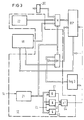
- FIG. 3 shows an exemplary embodiment for the control device ST explained with reference to FIG. 2 and its connection to the circuit elements specified in FIG. 2.
- message cells of fixed length and empty cells corresponding to these are transmitted during transmission pauses.
- the control device ST has a first counter arrangement Z1 which is connected to the control line SL (FIG. 2) and which is controlled by a control signal transmitted via this control line is synchronized and rotates with a counting period corresponding to the number of octets occurring in a message cell or empty cell.
- three fixed counter readings are provided as address signals by this counter arrangement.
- These address signals are delivered to three AND gates G1 to G3, each of which responds to one of these address signals.
- the AND gates are also acted upon jointly by clock pulses CL, so that a predetermined number of clock pulses are provided by these AND gates in succession within a message cell or empty cell, which are supplied to the bit rate memory BSP as write pulses via a downstream OR gate G4.
- the address signals provided by the counter arrangement Z1 are output to control inputs of the multiplexer M, shown schematically in FIG. 2, serving as an address multiplexer, and of a data multiplexer DM assigned to the latter.
- the outputs of these multiplexers are brought up to address and data inputs of the bit rate memory BSP.
- a second counter arrangement Z2 and an address bus of a switching computer VR superordinate to all treatment devices BHE (FIG. 1) are connected to the multiplexer M via three line systems in addition to the decoder DEC already shown in FIG.
- the counter arrangement Z2 which rotates with a counting period corresponding to the number of memory areas in the bit rate memory BSP, continuously provides address signals in accordance with the duration of an above-mentioned, periodically repeated memory cycle.
- a fixed initial counter reading for example in the form of a binary value "0"
- a data bus of the switching computer VR are brought in to the data multiplexer DM via three line systems on the input side.
- the address signals emitted by the counter arrangement Z1 define three separate processing time periods within a message cell or empty cell.
- a first of the processing time periods during which the decoder DEC and the register Reg3 are connected to the bit rate memory BSP via the multiplexers M and DM is used when a message cell occurs for reading out the assigned counter reading and the specified bit rate value from the bit rate memory and for the subsequent one Write the updated counter reading into this bit rate memory.
- a second processing period during which the counter arrangement Z2 and the provided initial counter reading are connected to the bit rate memory via the multiplexers M and DM is for the periodically provided interrogation of the counter readings stored in the bit rate memory and for the subsequent transfer of the respective one Meter reading reserved in the specified initial meter reading. Since address signals are continuously provided by the counter arrangement Z2, in the course of a storage cycle extending over a plurality of message cells or empty cells, a query and subsequent transfer to the initial counter reading takes place for all counter readings stored in the bit rate memory BSP. The evaluation of the individual queried meter readings is done by the switching computer VR.
- the switching computer VR is connected to the bit rate memory BSP with its address bus and data bus via the multiplexers M and DM.
- this switching computer can, on the one hand, enter the above-mentioned initial counter reading and the bit rate value specified for this virtual connection into the memory area of the bit rate memory in question when a virtual connection is established.
- the bit rate value in question for it and the associated current counter reading in the bit rate memory can be deleted.
- control device ST just explained is merely an expedient exemplary embodiment.
- functions to be performed by this control device can also be implemented by a different circuit design.
Landscapes
- Engineering & Computer Science (AREA)
- Computer Networks & Wireless Communication (AREA)
- Signal Processing (AREA)
- Data Exchanges In Wide-Area Networks (AREA)
- Communication Control (AREA)
- Use Of Switch Circuits For Exchanges And Methods Of Control Of Multiplex Exchanges (AREA)
Claims (5)
- Montage destiné à vérifier que les débits binaires de transmission fixés pour des communications virtuelles sont respectés lors de la transmission de cellules d'informations suivant un procédé de transmission asynchrone au cours des communications virtuelles dans une installation (BVA) de commutation ATM recevant les cellules d'informations par l'intermédiaire de circuits (E1,...,En) d'arrivée, à l'aide de dispositifs (BSP, Reg2, Reg3, ADD) de comptage associés aux circuits d'arrivée,dans lequel il est associé aux circuits d'arrivée, des dispositifs de comptage, qui sont en un nombre correspondant au nombre de communications virtuelles s'effectuant par ces circuits d'arrivée, qui sont formés de sorte queces dispositifs de comptage puissent être commandés individuellement lors de l'apparition de cellules d'informations en fonction d'un en-tête de cellule compris dans chacune de ces cellules et désignant la communication virtuelle respective, pendant la durée de transmission de la cellule d'information, qu'ainsi, l'état de comptage instantané de chaque dispositif de comptage soit changé d'une valeur fixée et qu'il soit fourni par le dispositif de comptage considéré, lorsque son état de comptage instantané est supérieur à une valeur limite fixée, un signal d'avertissement correspondant ou que la présence d'un signal d'avertissement de ce genre puisse être contrôlée,
caractérisé en ce que les dispositifs (BSP, Reg2, Reg3, ADD) de comptage sont perfectionnés par le fait que ceux-ci sont prévus exclusivement pour un dispositif de comptage unidirectionnel et passent à un état de comptage initial de manière répétée, périodiquement et à des intervalles de temps fixés,à chaque commande du dispositif de comptage considéré, son état de comptage instantané est changé au moins une fois, pendant l'apparition de la cellule d'information, d'une valeur de débit binaire, qui correspond au débit binaire de transmission fixé pour la communication virtuelle considérée,la valeur limite pour le dispositif de comptage considéré est fixée en fonction de la valeur du débit binaire associée à la communication virtuelle considérée et de la durée des intervalles de temps etéventuellement le signal d'avertissement est fourni ou la présence d'un signal d'avertissement de ce genre peut être contrôlée avant le passage du dispositif de comptage considéré à l'état de comptage initial. - Montage suivant la revendication 1,
caractérisé en ce que
les dispositifs (BSP, Reg2, Reg3, ADD) de comptage sont perfectionnés de sorte qu'à la suite d'une commande, s'effectuant à l'apparition d'une cellule d'information, d'un des dispositifs de comptage, son état de comptage instantané peut être changé, suivant un nombre fixé de bits appartenant à la cellule d'information qui vient d'apparaître, de la valeur de débit binaire qui est à la disposition du dispositif de comptage considéré. - Montage suivant la revendication 1 ou 2,
caractérisé en ce queune valeur ("1") normée de débit binaire est associée à un débit binaire de transmission pouvant être fixé au maximum,un état de comptage maximum uniforme est fixé pour tous les dispositifs (BSP, Reg2, Reg3, ADD) de comptage en fonction de cette valeur normée de débit binaire et de la durée fixée des intervalles de temps,et pour un débit binaire de transmission actuel s'écartant du débit binaire de transmission pouvant être fixé au maximum, la valeur de débit binaire associée est un multiple de la valeur normée de débit binaire, lequel correspond au rapport du débit binaire de transmission pouvant être fixé au maximum au débit binaire de transmission actuel. - Montage suivant la revendication 1 ou 2,
caractérisé en ce que
la valeur de débit binaire et l'état maximum de comptage sont fixés séparément pour chacun des dispositifs de comptage en fonction du débit binaire de transmission fixé pour la communication virtuelle considérée et de la durée fixée des intervalles de temps. - Montage suivant l'une des revendications 1 à 3,
caractérisé en ce queles dispositifs de comptage associés à un circuit d'arrivée sont formés de telle sorte queils soient formés chacun d'une zone de mémoire individuelle, qui sert à la mémorisation de la valeur de débit binaire associée pour la communication virtuelle considérée et à la mémorisation de l'état de comptage instantané, cette zone de mémoire individuelle étant celle d'une mémoire (BSP) à écriture-lecture, ainsi que d'un dispositif (Reg2, Reg3, ADD) d'addition relié à la mémoire d'écriture-lecture et commun à tous les dispositifs de comptage,un état comptage initial fixé puisse être introduit de manière répétée et périodique comme état de comptage instantané dans les zones de mémoire au cours d'un cycle de mémorisation activé à partir d'un dispositif (ST) de commande et incluant toutes les zones de mémoire,les diverses zones de mémoire puissent être englobées individuellement, lors de l'apparition de cellules d'informations, en fonction de l'en-tête de cellule contenu dans celles-ci, pour la durée de transmission de la cellule d'information considérée, dans un cycle de commande, au cours duquel l'état de comptage instantané qui vient d'être mémorisé dans la zone de mémoire considérée et la valeur de débit binaire, associée à celui-ci, sont envoyés au dispositif d'addition (Reg2, Reg3, ADD) pour un changement de l'état de comptage instantané concerné et ensuite, l'état de comptage instantané tenu prêt par le dispositif d'addition est introduit dans la zone de mémoire en réenregistrant à la place de l'état de comptage instantané mémorisé jusqu'à présent dans cette zone,un signal d'avertissement indiquant le dépassement du débit binaire de transmission fixé pour la communication virtuelle considérée est tenu prêt séparément à partir du dispositif d'addition, lorsque l'état de comptage instantané justement tenu prêt est plus grand que l'état de comptage maximum fixé.
Applications Claiming Priority (2)
| Application Number | Priority Date | Filing Date | Title |
|---|---|---|---|
| DE3932606 | 1989-09-29 | ||
| DE3932606 | 1989-09-29 |
Publications (3)
| Publication Number | Publication Date |
|---|---|
| EP0419959A2 EP0419959A2 (fr) | 1991-04-03 |
| EP0419959A3 EP0419959A3 (en) | 1992-07-01 |
| EP0419959B1 true EP0419959B1 (fr) | 1996-04-03 |
Family
ID=6390523
Family Applications (1)
| Application Number | Title | Priority Date | Filing Date |
|---|---|---|---|
| EP90117685A Expired - Lifetime EP0419959B1 (fr) | 1989-09-29 | 1990-09-13 | Circuit pour contrÔler le respet de débits préétablis lors de la transmission de cellules de données |
Country Status (4)
| Country | Link |
|---|---|
| US (1) | US5117417A (fr) |
| EP (1) | EP0419959B1 (fr) |
| AT (1) | ATE136409T1 (fr) |
| DE (1) | DE59010253D1 (fr) |
Families Citing this family (23)
| Publication number | Priority date | Publication date | Assignee | Title |
|---|---|---|---|---|
| DE58907901D1 (de) * | 1989-03-03 | 1994-07-21 | Siemens Ag | Verfahren und Schaltungsanordnung zum Weiterleiten von auf Zubringerleitungen übertragenen Nachrichtenpaketen über eine Paketvermittlungseinrichtung. |
| ATE127988T1 (de) * | 1990-03-23 | 1995-09-15 | Siemens Ag | Verfahren zum einrichten von virtuellen verbindungen in nach einem asynchronen transfermodus arbeitenden vermittlungseinrichtungen. |
| US5313455A (en) * | 1990-04-23 | 1994-05-17 | Koninklijke Ptt Nederland N.V. | Transmission system with recording of untransmitted packets |
| JPH04138743A (ja) * | 1990-09-29 | 1992-05-13 | Toshiba Corp | トラヒック監視方式 |
| DE59010139D1 (de) * | 1990-10-29 | 1996-03-28 | Siemens Ag | Verfahren zur Überwachung von einer Bitrate von wenigstens einer virtuellen Verbindung |
| JP3073249B2 (ja) * | 1991-03-20 | 2000-08-07 | 富士通株式会社 | Atm交換機における通過セル監視方式 |
| US5321692A (en) * | 1991-04-09 | 1994-06-14 | Siemens Aktiengesellschaft | Method for checking the admissibility of setting up virtual connections |
| FR2678122B1 (fr) * | 1991-06-18 | 1993-09-03 | Cit Alcatel | Dispositif de mesure de debit de circuits virtuels empruntant une voie de communication a multiplexage temporel asynchrone. |
| US5500853A (en) * | 1992-04-02 | 1996-03-19 | Applied Digital Access, Inc. | Relative synchronization system for a telephone network |
| DE59209493D1 (de) * | 1992-06-30 | 1998-10-15 | Siemens Ag | Modifiziertes Leaky-Bucket-Verfahren |
| US5523998A (en) * | 1993-04-14 | 1996-06-04 | Digital Equipment Corporation | Configuration controller for establishing timing signals of a communications network |
| JP2906361B2 (ja) * | 1993-09-01 | 1999-06-21 | 富士通株式会社 | 多重化制御方式 |
| JPH0779226A (ja) * | 1993-09-07 | 1995-03-20 | Fujitsu Ltd | 複数チャネル送出セル帯域制御回路 |
| CA2127521C (fr) * | 1994-07-06 | 2002-02-05 | Kenneth M. Buckland | Methode et dispositif de recuperation d'une horloge de service a debit binaire variable |
| DE4447240C1 (de) * | 1994-12-30 | 1996-05-23 | Siemens Ag | Verfahren und Schaltungsanordnung zum Überwachen festgelegter Übertragungsbitraten bei der Übertragung von Nachrichtenzellen |
| US5835711A (en) * | 1995-02-01 | 1998-11-10 | International Business Machines Corporation | Method and system for implementing multiple leaky bucket checkers using a hybrid synchronous/asynchronous update mechanism |
| US5761191A (en) * | 1995-11-28 | 1998-06-02 | Telecommunications Techniques Corporation | Statistics collection for ATM networks |
| JPH09284283A (ja) * | 1996-04-18 | 1997-10-31 | Mitsubishi Electric Corp | Atmプロトコル処理方法及びatmプロトコル処理装置 |
| US6791943B1 (en) * | 1998-02-27 | 2004-09-14 | Agilent Technologies, Inc. | Event-based technique for determining instantaneous cell bandwidth in a digital communications network |
| US6633545B1 (en) | 1999-07-30 | 2003-10-14 | Cisco Technology, Inc. | System and method for determining the data rate capacity of digital subscriber lines |
| US6636603B1 (en) | 1999-07-30 | 2003-10-21 | Cisco Technology, Inc. | System and method for determining the transmit power of a communication device operating on digital subscriber lines |
| US6631120B1 (en) | 1999-07-30 | 2003-10-07 | Cisco Technology, Inc. | System and method for determining a communication protocol of a communication device operating on digital subscriber lines |
| US7336667B2 (en) * | 2002-11-21 | 2008-02-26 | International Business Machines Corporation | Apparatus, method and program product to generate and use CRC in communications network |
Family Cites Families (8)
| Publication number | Priority date | Publication date | Assignee | Title |
|---|---|---|---|---|
| US4218756A (en) * | 1978-06-19 | 1980-08-19 | Bell Telephone Laboratories, Incorporated | Control circuit for modifying contents of packet switch random access memory |
| DE3036649A1 (de) * | 1980-09-29 | 1982-05-13 | Siemens AG, 1000 Berlin und 8000 München | Fernsprechvermittlungsnetz zur digitalen sprachuebertragung |
| US4641302A (en) * | 1985-06-24 | 1987-02-03 | Racal Data Communications Inc. | High speed packet switching arrangement |
| DE3778570D1 (de) * | 1986-03-14 | 1992-06-04 | Siemens Ag | Verfahren und schaltungsanordnung zum ueberwachen von mit einer datenvermittlungs- bzw. datenuebertragungseinrichtung verbundenen anschlussleitungen. |
| US4761800A (en) * | 1987-03-02 | 1988-08-02 | American Telephone And Telegraph Company, At&T Bell Laboratories | Method and apparatus for detecting a rate of data transmission |
| FR2616024B1 (fr) * | 1987-05-26 | 1989-07-21 | Quinquis Jean Paul | Systeme et methode de controle de flux de paquets |
| DE3732937A1 (de) * | 1987-09-30 | 1989-04-20 | Philips Patentverwaltung | Schaltungsanordnung zur vermeidung von ueberlast in einem breitband-vermittlungssystem |
| EP0329005B1 (fr) * | 1988-02-19 | 1993-11-03 | Siemens Aktiengesellschaft | Procédé pour l'établissement de circuits virtuels à travers les commutateurs d'un dispositif de commutation à plusieurs étages |
-
1990
- 1990-09-13 EP EP90117685A patent/EP0419959B1/fr not_active Expired - Lifetime
- 1990-09-13 DE DE59010253T patent/DE59010253D1/de not_active Expired - Fee Related
- 1990-09-13 AT AT90117685T patent/ATE136409T1/de not_active IP Right Cessation
- 1990-09-25 US US07/588,038 patent/US5117417A/en not_active Expired - Fee Related
Also Published As
| Publication number | Publication date |
|---|---|
| DE59010253D1 (de) | 1996-05-09 |
| ATE136409T1 (de) | 1996-04-15 |
| US5117417A (en) | 1992-05-26 |
| EP0419959A3 (en) | 1992-07-01 |
| EP0419959A2 (fr) | 1991-04-03 |
Similar Documents
| Publication | Publication Date | Title |
|---|---|---|
| EP0419958B1 (fr) | Circuit dans un central de commutation à multiplexage temporel asynchrone pour détecter la quantité de données transmises et pour contrÔler la conformité avec des taux de bits specifiés | |
| DE3856370T2 (de) | Vermittlungssystem und Verfahren zur Konstruktion davon | |
| EP0419959A2 (fr) | Circuit pour contrôler le respet de débits préétablis lors de la transmission de cellules de données | |
| EP0470283B1 (fr) | Méthode et dispositif pour déterminer la qualité de circuits virtuels transitant par un dispositif de commutation ATM | |
| EP0483397B1 (fr) | Méthode pour contrÔler le débit binaire d'au moins un circuit virtuel | |
| EP0566961B1 (fr) | Procédé et circuit pour faire respecter le débit de transmission préaccordé dans un dispositif de commutation ATM | |
| DE2503111B2 (de) | Verfahren und schaltungsanordnung zur zeitmultiplexen uebertragung von nutzinformationen aus voneinander unabhaengigen quellen | |
| DE69028266T2 (de) | Paketvermittlungsnetzwerk für unterschiedliche Typen von Paketen | |
| EP0329005B1 (fr) | Procédé pour l'établissement de circuits virtuels à travers les commutateurs d'un dispositif de commutation à plusieurs étages | |
| DE69011710T2 (de) | Verfahren zur ATD (asynchronous time division)-Vermittlung von Datenpaketen und Anordnung zur Durchführung dieses Verfahrens. | |
| DE3732937A1 (de) | Schaltungsanordnung zur vermeidung von ueberlast in einem breitband-vermittlungssystem | |
| EP0453607A1 (fr) | Méthode et dispositif pour réduire la perte de paquets d'information, transmis par un commutateur de paquets | |
| DE60000023T2 (de) | Vom Rechenaufwand her effizientes Verkehrsformer | |
| EP0730362A2 (fr) | Méthode et circuit pour le transfert de paquets de données, transmises par un système ATM, à une ligne de sortie | |
| DE4434724C1 (de) | Verfahren und Schaltungsanordnung zum Weiterleiten von einer ATM-Kommunikationseinrichtung zugeführten Nachrichtenzellen | |
| EP0351014B1 (fr) | Réseau de commutation pour système de commutation | |
| DE2515801A1 (de) | Verfahren und schaltungsanordnungen zur zeitmultiplexen datenuebertragung | |
| DE69014432T2 (de) | Verfahren und Vorrichtung zur quantisierten Flussberechnung virtueller Verbindungen über einen asynchronen Zeitmultiplexübertragungsweg. | |
| EP0730361A2 (fr) | Circuit pour la réception et le transfert de paquets de données par un réseau ATM | |
| DE69509499T2 (de) | Verfahren und einrichtung zur übertragung zwischen knoten in einem kommunikationsnetzwerk | |
| EP0523276B1 (fr) | Procédé et circuit pour arranger des liaisons virtuelles à travers un faisceau de lignes de liaison-ATM (mode de transfert asynchrone) | |
| EP0763914A2 (fr) | Procédé et arrangement d'adaptation de la vitesse de bit de transmission d'un dispositif de multiplexage de données travaillant selon le mode de transfert asynchrone | |
| EP0720411B1 (fr) | Méthode et système pour la surveillance d'un courant de cellules ATM | |
| EP0173274B1 (fr) | Méthode et montage pour la réalisation et la maintenance d'une liaison à division temporelle à large bande | |
| DE19911830A1 (de) | Verfahren zum Verwalten des Zugriffs auf einen Bus und Bussystem |
Legal Events
| Date | Code | Title | Description |
|---|---|---|---|
| PUAI | Public reference made under article 153(3) epc to a published international application that has entered the european phase |
Free format text: ORIGINAL CODE: 0009012 |
|
| 17P | Request for examination filed |
Effective date: 19901205 |
|
| AK | Designated contracting states |
Kind code of ref document: A2 Designated state(s): AT BE CH DE FR GB IT LI NL SE |
|
| PUAL | Search report despatched |
Free format text: ORIGINAL CODE: 0009013 |
|
| AK | Designated contracting states |
Kind code of ref document: A3 Designated state(s): AT BE CH DE FR GB IT LI NL SE |
|
| 17Q | First examination report despatched |
Effective date: 19940429 |
|
| GRAH | Despatch of communication of intention to grant a patent |
Free format text: ORIGINAL CODE: EPIDOS IGRA |
|
| GRAA | (expected) grant |
Free format text: ORIGINAL CODE: 0009210 |
|
| AK | Designated contracting states |
Kind code of ref document: B1 Designated state(s): AT BE CH DE FR GB IT LI NL SE |
|
| REF | Corresponds to: |
Ref document number: 136409 Country of ref document: AT Date of ref document: 19960415 Kind code of ref document: T |
|
| REG | Reference to a national code |
Ref country code: CH Ref legal event code: NV Representative=s name: SIEMENS SCHWEIZ AG |
|
| REF | Corresponds to: |
Ref document number: 59010253 Country of ref document: DE Date of ref document: 19960509 |
|
| ITF | It: translation for a ep patent filed | ||
| GBT | Gb: translation of ep patent filed (gb section 77(6)(a)/1977) |
Effective date: 19960618 |
|
| ET | Fr: translation filed | ||
| PGFP | Annual fee paid to national office [announced via postgrant information from national office to epo] |
Ref country code: GB Payment date: 19960821 Year of fee payment: 7 |
|
| PGFP | Annual fee paid to national office [announced via postgrant information from national office to epo] |
Ref country code: AT Payment date: 19960904 Year of fee payment: 7 |
|
| PGFP | Annual fee paid to national office [announced via postgrant information from national office to epo] |
Ref country code: BE Payment date: 19960911 Year of fee payment: 7 |
|
| PGFP | Annual fee paid to national office [announced via postgrant information from national office to epo] |
Ref country code: SE Payment date: 19960912 Year of fee payment: 7 |
|
| PGFP | Annual fee paid to national office [announced via postgrant information from national office to epo] |
Ref country code: NL Payment date: 19960916 Year of fee payment: 7 |
|
| PGFP | Annual fee paid to national office [announced via postgrant information from national office to epo] |
Ref country code: FR Payment date: 19960926 Year of fee payment: 7 |
|
| PGFP | Annual fee paid to national office [announced via postgrant information from national office to epo] |
Ref country code: DE Payment date: 19961118 Year of fee payment: 7 |
|
| PGFP | Annual fee paid to national office [announced via postgrant information from national office to epo] |
Ref country code: CH Payment date: 19961216 Year of fee payment: 7 |
|
| PLBE | No opposition filed within time limit |
Free format text: ORIGINAL CODE: 0009261 |
|
| STAA | Information on the status of an ep patent application or granted ep patent |
Free format text: STATUS: NO OPPOSITION FILED WITHIN TIME LIMIT |
|
| 26N | No opposition filed | ||
| PG25 | Lapsed in a contracting state [announced via postgrant information from national office to epo] |
Ref country code: GB Free format text: LAPSE BECAUSE OF NON-PAYMENT OF DUE FEES Effective date: 19970913 Ref country code: AT Free format text: LAPSE BECAUSE OF NON-PAYMENT OF DUE FEES Effective date: 19970913 |
|
| PG25 | Lapsed in a contracting state [announced via postgrant information from national office to epo] |
Ref country code: SE Free format text: LAPSE BECAUSE OF NON-PAYMENT OF DUE FEES Effective date: 19970914 |
|
| PG25 | Lapsed in a contracting state [announced via postgrant information from national office to epo] |
Ref country code: LI Free format text: LAPSE BECAUSE OF NON-PAYMENT OF DUE FEES Effective date: 19970930 Ref country code: FR Free format text: THE PATENT HAS BEEN ANNULLED BY A DECISION OF A NATIONAL AUTHORITY Effective date: 19970930 Ref country code: CH Free format text: LAPSE BECAUSE OF NON-PAYMENT OF DUE FEES Effective date: 19970930 Ref country code: BE Free format text: LAPSE BECAUSE OF NON-PAYMENT OF DUE FEES Effective date: 19970930 |
|
| BERE | Be: lapsed |
Owner name: SIEMENS A.G. Effective date: 19970930 |
|
| PG25 | Lapsed in a contracting state [announced via postgrant information from national office to epo] |
Ref country code: NL Free format text: LAPSE BECAUSE OF NON-PAYMENT OF DUE FEES Effective date: 19980401 |
|
| GBPC | Gb: european patent ceased through non-payment of renewal fee |
Effective date: 19970913 |
|
| REG | Reference to a national code |
Ref country code: CH Ref legal event code: PL |
|
| NLV4 | Nl: lapsed or anulled due to non-payment of the annual fee |
Effective date: 19980401 |
|
| PG25 | Lapsed in a contracting state [announced via postgrant information from national office to epo] |
Ref country code: DE Free format text: LAPSE BECAUSE OF NON-PAYMENT OF DUE FEES Effective date: 19980603 |
|
| EUG | Se: european patent has lapsed |
Ref document number: 90117685.9 |
|
| REG | Reference to a national code |
Ref country code: FR Ref legal event code: ST |
|
| PG25 | Lapsed in a contracting state [announced via postgrant information from national office to epo] |
Ref country code: IT Free format text: LAPSE BECAUSE OF NON-PAYMENT OF DUE FEES Effective date: 20050913 |