EP0420183B1 - Circuit push-pull - Google Patents
Circuit push-pull Download PDFInfo
- Publication number
- EP0420183B1 EP0420183B1 EP90118465A EP90118465A EP0420183B1 EP 0420183 B1 EP0420183 B1 EP 0420183B1 EP 90118465 A EP90118465 A EP 90118465A EP 90118465 A EP90118465 A EP 90118465A EP 0420183 B1 EP0420183 B1 EP 0420183B1
- Authority
- EP
- European Patent Office
- Prior art keywords
- transistor
- current
- circuit
- push
- transistors
- Prior art date
- Legal status (The legal status is an assumption and is not a legal conclusion. Google has not performed a legal analysis and makes no representation as to the accuracy of the status listed.)
- Expired - Lifetime
Links
- 238000001514 detection method Methods 0.000 claims description 3
- 101100299614 Homo sapiens PTPN13 gene Proteins 0.000 claims 18
- 101100352663 Mus musculus Pnp gene Proteins 0.000 claims 18
- 101150069896 PNP1 gene Proteins 0.000 claims 18
- 102100033014 Tyrosine-protein phosphatase non-receptor type 13 Human genes 0.000 claims 18
- 102000004207 Neuropilin-1 Human genes 0.000 claims 6
- 108090000772 Neuropilin-1 Proteins 0.000 claims 6
- 101100244438 Alkaliphilus metalliredigens (strain QYMF) pnp3 gene Proteins 0.000 claims 5
- 101100244439 Alkaliphilus metalliredigens (strain QYMF) pnp4 gene Proteins 0.000 claims 5
- 101000704557 Homo sapiens Sulfiredoxin-1 Proteins 0.000 claims 5
- 102100031797 Sulfiredoxin-1 Human genes 0.000 claims 5
- 230000003247 decreasing effect Effects 0.000 claims 2
- 102000004213 Neuropilin-2 Human genes 0.000 claims 1
- 108090000770 Neuropilin-2 Proteins 0.000 claims 1
- 230000007274 generation of a signal involved in cell-cell signaling Effects 0.000 description 14
- 238000010586 diagram Methods 0.000 description 7
- 238000010276 construction Methods 0.000 description 4
- 230000009467 reduction Effects 0.000 description 4
- 230000000694 effects Effects 0.000 description 3
- 239000004065 semiconductor Substances 0.000 description 3
- 230000002159 abnormal effect Effects 0.000 description 1
- 230000008859 change Effects 0.000 description 1
- 230000000295 complement effect Effects 0.000 description 1
- 238000000034 method Methods 0.000 description 1
- 230000004048 modification Effects 0.000 description 1
- 238000012986 modification Methods 0.000 description 1
- 238000004886 process control Methods 0.000 description 1
- 230000035945 sensitivity Effects 0.000 description 1
- 230000003068 static effect Effects 0.000 description 1
Images



Classifications
-
- H—ELECTRICITY
- H03—ELECTRONIC CIRCUITRY
- H03F—AMPLIFIERS
- H03F3/00—Amplifiers with only discharge tubes or only semiconductor devices as amplifying elements
- H03F3/26—Push-pull amplifiers; Phase-splitters therefor
-
- H—ELECTRICITY
- H03—ELECTRONIC CIRCUITRY
- H03F—AMPLIFIERS
- H03F3/00—Amplifiers with only discharge tubes or only semiconductor devices as amplifying elements
- H03F3/30—Single-ended push-pull [SEPP] amplifiers; Phase-splitters therefor
- H03F3/3001—Single-ended push-pull [SEPP] amplifiers; Phase-splitters therefor with field-effect transistors
-
- H—ELECTRICITY
- H03—ELECTRONIC CIRCUITRY
- H03F—AMPLIFIERS
- H03F1/00—Details of amplifiers with only discharge tubes, only semiconductor devices or only unspecified devices as amplifying elements
- H03F1/32—Modifications of amplifiers to reduce non-linear distortion
- H03F1/3217—Modifications of amplifiers to reduce non-linear distortion in single ended push-pull amplifiers
Definitions
- the present invention relates to a push-pull circuit of the type described in the preamble part of claim 1.
- a push-pull circuit is used in an output circuit of a semiconductor integrated circuit.
- a push-pull circuit of the type mentioned hereinabove is disclosed in US-A-4 737 732.
- a P-channel MOS transistor P1 and an N-channel MOS transistor N1 are serially connected between a power source potential Vcc and a ground potential GND to constitute a push-pull output stage circuit.
- An output terminal OUT is connected to a connection node between the P-channel MOS transistor P1 and N-channel MOS transistor N1.
- a current source circuit 71, a level shift circuit 72 and an N-channel MOS transistor N2 are serially connected between the Vcc potential and GND potential.
- the gate of the N-channel MOS transistor N2 for output control is connected to an input terminal IN to which an input signal is supplied.
- a connection node Ne between the current source circuit 71 and the level shift circuit 72 is connected to the gate of the P-channel MOS transistor P1.
- a connection node Nf between the level shift circuit 72 and the N-channel MOS transistor N2 is connected to the gate of the N-channel MOS transistor N1.
- the push-pull output circuit shown in Fig. 2 is different from that of Fig. 1 in that the level shift circuit 72 is omitted, and a P-channel MOS transistor P2 and a second current source circuit 81 are connected between the Vcc potential and the GND potential.
- the gate of the N-channel MOS transistor N2 is connected to the input terminal IN.
- a connection node Ng between the gate and drain of the P-channel MOS transistor P2 is connected to the gate of the P-channel MOS transistor P1.
- a connection node Nh between the first current source circuit 71 and the N-channel MOS transistor N2 is connected to the gate of the N-channel MOS transistor N1.
- the level shift amount (a difference between the potential of the node Ne and the potential of the node Nf) of the level shift circuit 72 is fixed and cannot be adjusted. Therefore, the bias voltage (voltage between the source and gate) of the two MOS transistors P1 and N1 varies substantially in proportion to variation in the Vcc potential. As a result, an ineffective current (which is a current flowing in the MOS transistors P1 and N1 when the output terminal OUT is set in the electrically floating state; static current; DC current) flowing in the two MOS transistors P1 and N1 constituting the push-pull output stage circuit will vary. Thus, the power consumption in the push-pull output circuit varies and the characteristic of the circuit also varies.
- the push-pull circuit of Fig. 1 it is necessary to use a constant voltage source whose output voltage is stable. Further, the ineffective current flowing in the push-pull output stage circuit may be largely influenced by variation in the threshold voltage of the MOS transistors P1 and N1. When attempts are made to suppress variation in the ineffective current, the process control may become severer or the yield of the semiconductor device will be lowered.
- the P-channel MOS transistors P1 and P2 are connected in a current mirror configuration.
- the gate of the P-channel MOS transistor P1 is always applied with a constant bias voltage from the gate of the P-channel MOS transistor P2, thereby causing a constant current to always flow in the P-channel MOS transistor P1.
- the maximum value of the output current in the push-pull output circuit becomes equal to that of a constant current flowing in the P-channel MOS transistor P1. Therefore, when a large output current is required, it becomes necessary to set the ineffective current at the time of no load to a large value, making a power consumption larger.
- a push-pull circuit according to the invention may comprise an output circuit having first and second transistors whose current paths are serially connected between a first potential and a second potential, and potenial difference setting means for detecting a current level of at least one of currents flowing in the first and second transistors and setting a potential difference between signals supplied to the control terminals of the first and second transistors according to the result of detection.
- the push-pull circuit according to the present invention it becomes possible to keep an ineffective current flowing in the transistors of the output stage circuit constant, irrespective of or less influenced by variations in the power source voltage and the characteristics of the transistors.
- the push-pull circuit according to the invention has a high performance.
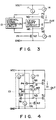
- Fig. 3 shows a push-pull output circuit of CMOS structure used in the output circuit of a semiconductor integrated circuit which requires a large amplitude characteristic, less distortion characteristic and large output current characteristic.
- the push-pull output circuit includes a push-pull output stage circuit constituted by a P-channel MOS transistor P1 and an N-channel MOS transistor N1 which are serially connected between a power source potential Vcc and a ground potential GND.
- the MOS transistors P1 and N1 have complementary characteristics. Further, as shown in Fig. 5, when the gate-source voltage VGS increases, the drain current increases in a quadratic manner.
- the push-pull output circuit includes a first constant current source circuit 11, level shift circuit 12 and N-channel MOS transistor N2 for output control which are serially connected between the Vcc potential and the GND potential.
- a connection node Na between the first constant current source circuit 11 and level shift circuit 12 is connected to the control electrode (gate) of the MOS transistor P1.
- a connection node Nb between the level shift circuit 12 and output controlling MOS transistor N2 is connected to the gate of the MOS transistor N1.
- the push-pull output circuit includes a control signal generation circuit 13.
- reference numerals 14 and 15 denote circuits for detecting currents flowing in the two MOS transistors P1 and N1 of the push-pull output stage circuit and constituting part of the control signal generation circuit 13.
- the MOS transistor N2 is turned on or off according to the level of a signal supplied to the input terminal IN.
- the gate potentials of the MOS transistors P1 and N1 vary according to the on-off operation of the MOS transistor so that the resistance of the current paths of the MOS transistors P1 and N1 may be changed.
- an output signal having a level corresponding to the level of the input signal is output from the output terminal OUT.
- the potential of the output signal greatly varies between the ground potential GND and the power source potential Vcc.
- the level shift circuit 12 adjusts (changes) the level shift amount (a potential difference between the nodes Na and Nb) according to a control signal supplied from the control signal generation circuit 13.
- the control signal generation circuit 13 detects the current level of a current flowing in the MOS transistors P1 and N1 by means of the circuits 14 and 15.
- the control signal generation circuit 13 supplies a control signal to the level shift circuit 12 to control the level shift amount of the level shift circuit 12 according to the detected current values so as to keep ineffective currents flowing in the MOS transistors P1 and N1 constant. For example, the control signal generation circuit 13 increases the level shift amount when the current level flowing in the MOS transistors P1 and N1 is raised.
- the control signal generation circuit 13 reduces the level shift amount when the current level of a current flowing in the MOS transistors P1 and N1 is lowered.
- the gate-source voltage of the MOS transistors P1 and N1 is raised, thereby causing the current flowing in the MOS transistors P1 and N1 to be increased.
- the ineffective current flowing in the MOS transistors P1 and N1 can be kept constant.
- the level shift amount of the level shift circuit 12 is largely influenced by the magnitude of the output current and there occurs a possibility that the push-pull output circuit may effect an abnormal operation.
- the control signal generation circuit 13 has a characteristic of outputting a control signal which is created mainly according to a smaller one of the currents flowing in the MOS transistors P1 and N1.
- a control signal is created mainly according to a smaller one of the currents flowing in the MOS transistors P1 and N1.
- the control signal generation circuit 13 is designed to have a characteristic as shown in Fig. 6, the gate-source voltage VGS of that one of the MOS transistors which permits output or input current flow can be set to be sufficiently high, thus causing a relatively large output current to be derived.
- the level shift circuit 12 is constituted by a variable resistor formed of a P-channel MOS transistor P3 and an N-channel MOS transistor N3 whose current path is connected in parallel with the current path of the MOS transistor P3.
- the level shift circuit 12 effects the level shift operation according to a voltage drop caused across the current paths of the MOS transistors P3 and N3 by a current from the first constant current source circuit 11.
- the control signal generation circuit 13 is constituted by a P-channel MOS transistor P4, a second constant current source circuit 16, a third constant current source circuit 17 and an N-channel MOS transistor N4.
- the current path of the P-channel MOS transistor P4 and the second constant current source 16 are serially connected between the Vcc potential and the GND potential.
- the third constant current source circuit 17 and the current path of the N-channel MOS transistor N4 are serially connected between the Vcc potential and the GND potential.
- the gate of the P-channel MOS transistor P4 is connected to the connection node Na (the gate of the P-channel MOS transistor P1).
- the gate of the N-channel MOS transistor N4 is connected to the connection node Nb (the gate of the N-channel MOS transistor N1).
- a connection node (node Nc) between the P-channel MOS transistor P4 and the second constant current source circuit 16 is connected to the gate of the P-channel MOS transistor P3.
- a connection node (node Nd) between the third constant current source circuit 17 and the N-channel MOS transistor N4 is connected to the gate of the N-channel MOS transistor N3.
- the ratio of the W (channel width)/L (channel length) ratio of the MOS transistor P1 to a desired ineffective current is set to be the same as the ratio of the W/L ratio of the MOS transistor P4 to an output current of the constant current source circuit 16.
- the ratio of the W/L ratio of the MOS transistor N1 to a desired ineffective current is set to be the same as the ratio of the W/L ratio of the MOS transistor N4 to an output current of the constant current source circuit 17.
- the ineffective current is set to 500 mA
- the W/L ratio of the MOS transistor P1 is set to 10
- the W/L ratio of the MOS transistor P4 is set to 1
- the output current of the constant current source circuit 16 will be 50 mA.
- the MOS transistors of the same conductivity type are formed in the same step in order to make variations in the characteristics thereof such as variations in the threshold voltages thereof equal to one another.
- the basic operation of the circuit shown in Fig. 4 is the same as that of the circuit of Fig. 3 and a signal having a level corresponding to the level of the signal supplied to the input terminal IN is derived from the output terminal OUT.
- the gate-source voltage of the MOS transistor P1 is lowered. Since the same gate-source voltage as that of the MOS transistor P1 is applied to the MOS transistor P4, the resistance of the current path of the MOS transistor P4 increases. As a result, the potential of the drain (node Nc) of the MOS transistor P4 is lowered. Reduction in the potential causes the resistance of the P-channel MOS transistor P3 to be lowered.
- Reduction in the resistances of the current paths of the MOS transistors P3 and N3 constituting the level shift circuit 12 causes the potential of the node Na to be lowered, thereby raising the potential of the node Nb. That is, the level shift amount (a potential difference between the nodes Na and Nb) is reduced. Reduction in the level shift amount causes the source-gate voltage of the MOS transistors P1 and N1 to be raised.
- the gate-source voltage of the MOS transistor P1 increases. Since the same gate-source voltage as that of the MOS transistor P1 is applied to the MOS transistor P4, the resistance of the current path of the MOS transistor P4 increases. As a result, the potential of the drain (node Nc) of the MOS transistor P4 is raised. Rise in the potential causes the resistance of the P-channel MOS transistor P3 to increase.
- the potential of the node Na is raised and the potential of the node Nb is lowered with an increase in the resistances of the current paths of the MOS transistors P3 and N3 constituting the level shift circuit 12. That is, the level shift amount is increased. Increase in the level shift amount causes the gate-source voltages of the MOS transistors P1 and N1 to be lowered. As is understood from Fig. 5, with a decrease in the source-gate voltages of the MOS transistors P1 and N1, currents flowing in the MOS transistors P1 and N1 are reduced. As a result, the current can be kept constant irrespective of an increase in the power source voltage Vcc.
- the control signal generation circuit 13 shown in Fig. 4 also has a function of detecting only a smaller one of the currents and outputting a control signal based on the detected current.
- a current flowing in the MOS transistor P1 becomes larger than that in the MOS transistor N1.
- the resistance of the current path of the MOS transistor P4 is reduced, and the current in the MOS transistor P4 tends to increase.
- the current is limited to a preset value by means of the constant current source 16. Therefore, the potential of the node Nc is raised.
- the potential of the node Nc is applied to the gate of the P-channel MOS transistor P3 of the level shift circuit 12 and when the potential of the node Nc becomes equal to or higher than a preset level, the P-channel MOS transistor P3 is turned off. Therefore, even if a current flowing in the MOS transistor P1 becomes extremely large with an increase in the output current, the level shift amount of the level shift circuit 12 is not influenced by the output current when the current flowing in the MOS transistor P1 has exceeded the preset value.
- the level shift amount of the level shift circuit 12 is controlled by the current flowing in the MOS transistor N1 to keep the ineffective current flowing in the MOS transistor N1 constituting the push-pull output stage circuit at substantially a constant level.
- the level shift amount of the level shift circuit 12 is not influenced by the input current when the current flowing in the MOS transistor N1 has exceeded a preset value.
- the level shift amount of the level shift circuit 12 is controlled by the current flowing in the MOS transistor P1 to keep the ineffective current flowing in the MOS transistor P1 and N1 constituting the push-pull output stage circuit at substantially a constant level.
- the ineffective current can be kept at substantially a constant value even if the power source voltage and the characteristics of the MOS transistors have varied. Further, influence on the control signal generation circuit 13 by currents flowing out from the output terminal or flowing into the output terminal from the exterior can be removed.
- a curve A in Fig. 7 indicates the relation between the gate-source voltage VGS of the MOS transistor P1 of the push-pull output circuit shown in Fig. 4 and the power source voltage Vcc.
- the relations between the gate-source voltage VGS of the MOS transistor P1 of the conventional push-pull output circuit shown in Fig. 1 and the power source voltage Vcc are indicated by curves A' and A".
- a curve Vth indicates variation in the threshold voltage of the MOS transistor P1.
- a curve B of Fig. 8 indicates the relation between the ineffective current I1 in the MOS transistor P1 of the push-pull output circuit shown in Fig. 4 and the power source voltage Vcc.
- the relations between the ineffective current I1 in the MOS transistor P1 of the push-pull output circuit shown in Fig. 1 and the power source voltage Vcc are indicated by curves B' and B".
- the inclination of the characteristic curve A in Fig. 7 and the inclination of the characteristic curve B in Fig. 8 indicate variation in the current of the current source circuits 11, 16 and 17 in the push-pull output circuit of Fig. 4 and variation in the drain-source voltage of the MOS transistor P1.
- the bias voltage VGS and ineffective current I1 are kept substantially constant irrespective of variation in the power source voltage Vcc.
- the bias voltage VGS of the MOS transistor P1 varies with the power source voltage Vcc as indicated by the characteristic curve A'.
- the ineffective current I1 of the MOS transistor P1 exhibits the quadrant characteristic as indicated by the characteristic curve B' of Fig. 8 when the bias voltage VGS has exceeded the threshold voltage Vth of the MOS transistor P1.
- the curve A" of Fig. 7 shows a case wherein the threshold voltage Vth of the P-channel MOS transistor P1 has varied and indicates the bias voltage VGS of the P-channel MOS transistor P1 with the threshold voltage Vth set as a reference value.
- the ineffective current I1 is significantly varied.
- the threshold voltage Vth of the P-channel MOS transistor P1 of the push-pull output stage circuit has varied, the threshold voltage Vth of the P-channel MOS transistor P4 varies in the same manner so that the gate-source voltage of the P-channel MOS transistor P3 of the level shift circuit 12 will be kept unchanged and a voltage of the bias node Na can be kept unchanged.
- the construction of the push-pull output circuit is not limited to the above embodiment.
- an anti-oscillation circuit can be added to the above circuit, and it is also possible to set the size of the P-channel MOS transistor P4 and N-channel MOS transistor N4 to, for example, twice that of the MOS transistors P1 and N1 in order to enhance the sensitivity of detecting currents flowing in the two MOS transistors P1 and N1 of the push-pull output stage circuit.
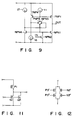
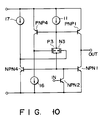
- MOS transistors are used as transistors, but it is also possible to use bipolar transistors or BiCMOS technique to constitute the circuits as shown in Figs. 9 and 10. In the construction of Fig. 9, substantially the same effect as that of the above embodiment can be obtained. Further, elements other than the MOS transistors and bipolar transistors may be used.
- MOS transistors of the same conductivity type are preferably formed in the same step in order to make equal variations in the characteristics such as variations in the threshold voltages. However, they may be formed in different steps.
- the output stage circuit may be formed as shown in Fig. 11, and the level shift circuit may be formed as shown in Fig. 12.
- the control signal generation circuit may be constructed to perform the operation based on data from the ammeters 14 and 15 so as to control the level shift amount, for example.
Landscapes
- Engineering & Computer Science (AREA)
- Power Engineering (AREA)
- Physics & Mathematics (AREA)
- Nonlinear Science (AREA)
- Logic Circuits (AREA)
- Amplifiers (AREA)
Claims (11)
- Circuit push-pull, comprenant :une borne d'entrée (IN) ;une borne de sortie (OUT) ;un circuit d'étage de sortie relié entre un premier potentiel (Vcc) et un second potentiel (GND) et ayant un premier transistor (P1 ; PNP1) d'un premier type de conductivité, un second transistor (N1 ; NPN1) d'un second type de conductivité dans lesquels des chemins de courant sont reliés en série, et ladite borne de sortie (OUT) reliée aux bornes de drain dudit premier transistor (P1 ; PNP1) et dudit second transistor (N1 ; NPN1) ;un circuit de décalage de niveau (12) ayant un troisième transistor (P3 ; PNP3) du premier type de conductivité et un quatrième transistor (N3 ; NPN3) dans lesquels un chemin de courant est relié en parallèle au chemin de courant dudit troisième transistor (P3 ; PNP3) du premier type de conductivité ;un circuit de commande (13) ayant un cinquième transistor (P4 ; PNP4) du premier type de conductivité et un premier circuit de source de courant (16) qui sont reliés en série entre lesdits premier et second potentiels, et un second circuit de source de courant (17) et un sixième transistor (N4 ; NPN4) du second type de conductivité qui sont reliés en série entre lesdits premier et second potentiels ;dans lequel une borne de commande dudit cinquième transistor (P4 ; PNP4) du premier type de conductivité est reliée à une borne de commande dudit premier transistor (P1 ; PNP1) du premier type de conductivité ;dans lequel une borne de commande dudit sixième transistor (N4 ; NPN4) du second type de conductivité est reliée à une borne de commande dudit second transistor (N1 ; NPN1) du second type de conductivité ;dans lequel un noeud de connexion entre ledit cinquième transistor (P4 ; PNP4) du premier type de conductivité et ledit premier circuit de source de courant (16) est relié à une borne de commande dudit troisième transistor (P3 ; PNP3) du premier type de conductivité ; etdans lequel un noeud de connexion entre ledit second circuit de source de courant (17) et ledit sixième transistor (N4 ; NPN4) du second type de conductivité est relié à une borne de commande dudit quatrième transistor (N3 ; NPN3) ;caractérisé en ce queledit quatrième transistor (N3 ; NPN3) est du second type de conductivité ;la borne de drain dudit troisième transistor (P3 ; PNP3) et la borne de source dudit quatrième transistor (N3 ; NPN3) sont reliées ensemble, comme le sont la borne de source dudit troisième transistor (P3 ; PNP3) et la borne de drain dudit quatrième transistor (N3 ; NPN3), ces deux connexions, respectivement, formant des premier et second ports communs ;lesdits premier et second ports communs étant respectivement reliés directement aux bornes de commande interconnectées desdits premier et cinquième transistors (P1 ; PNP1, P4 ; PNP4) et desdits second et sixième transistors (N1 ; NPN1, N4 ; NPN4) ;une troisième source de courant (11) est reliée entre ledit circuit de décalage de niveau (12) et ledit premier potentiel (Vcc) ; etun transistor de commande de sortie (N2 ; NPN2) a un chemin de courant relié entre la seconde partie commune dudit circuit de décalage de niveau (12) et ledit second potentiel (GND), et est relié par sa borne de commande à ladite borne d'entrée (IN).
- Circuit push-pull selon la revendication 1, caractérisé en ce quele rapport du rapport de largeur de canal/ longueur de canal dudit premier transistor (P1 ; PNP1) du premier type de conductivité sur un courant inefficace voulu est substantiellement égal au rapport du rapport de largeur de canal/longueur de canal dudit cinquième transistor (P4 ; PNP4) du premier type de conductivité sur un courant de sortie dudit premier circuit de source de courant (16) ; etle rapport du rapport de largeur de canal/ longueur de canal dudit second transistor (N1 ; NPN1) du second type de conductivité sur un courant inefficace voulu est substantiellement égal au rapport du rapport de largeur de canal/longueur de canal dudit sixième transistor (N4 ; NPN4) du second type de conductivité sur un courant de sortie dudit second circuit de source de courant (17).
- Circuit push-pull selon l'une quelconque des revendications précédentes, caractérisé en ce que ledit circuit de commande (13) comprend des circuits de détection de courant (14, 15) respectivement reliés auxdits premier et second transistors (P1, N1) pour détecter des niveaux de courant des courants passant dans lesdits premier et second transistors (P1, N1).
- Circuit push-pull selon l'une quelconque des revendications précédentes, caractérisé en ce que ledit circuit de décalage de niveau (12) et ledit circuit de commande (13) forment un dispositif de détection de niveau de courant et de réglage de différence de potentiel, pour détecter un niveau de courant d'au moins un des courants passant dans lesdits premier et second transistors (P1 ; PNP1, N1 ; NPN1), et pour régler une différence de potentiel entre des signaux appliqués aux bornes de commande desdits premier et second transistors (P1 ; PNP1, N1 ; NPN1) selon le résultat de la détection.
- Circuit push-pull selon la revendication 4, caractérisé en ce que ledit dispositif de réglage de différence de potentiel comprend un dispositif pour élever le potentiel lorsque les courants passant dans lesdits premier et second transistors (P1 ; PNP1, N1 ; PNP1) ont augmenté et abaisse le potentiel lorsque les courants passant dans lesdits premier et second transistors (P1 ; PNP1, N1 ; PNP1) ont diminué.
- Circuit push-pull selon la revendication 4, caractérisé en ce que ledit dispositif de réglage de différence de potentiel comprend un dispositif pour commander la tension de polarisation appliquée auxdits premier et second transistors (P1 ; PNP1, N1 ; PNP1) pour la maintenir à des valeurs constantes indépendamment de si les courants passant dans les premier et second ((P1 ; PNP1, N1 ; PNP1) ont augmenté ou diminué.
- Circuit push-pull selon la revendication 4, caractérisé en ce que ledit dispositif de réglage de différence de potentiel commande le potentiel selon le plus petit des courants passant dans lesdits premier et second transistors (P1 ; PNP1, N1 ; PNP1).
- Circuit push-pull selon l'une quelconque des revendications précédentes, caractérisé en ce que ladite troisième source de courant (11), ledit circuit de décalage de niveau (12) et ledit circuit de commande (13) sont fournis pour maintenir un courant inefficace passant dans ledit circuit push-pull à une valeur substantiellement constante.
- Circuit de sortie push-pull selon l'une quelconque des revendications précédentes, caractérisé en ce que ledit premier potentiel (Vcc) est un potentiel de source d'alimentation et ledit second potentiel (GND) est un potentiel de masse.
- Circuit push-pull selon l'une quelconque des revendications 1 à 9, caractérisé en ce que lesdits premier au sixième transistors sont formés de transistors MOS.
- Circuit push-pull selon l'une quelconque des revendications 1 à 9, caractérisé en ce que lesdits premier au sixième transistors sont formés de transistors bipolaires.
Applications Claiming Priority (2)
| Application Number | Priority Date | Filing Date | Title |
|---|---|---|---|
| JP249076/89 | 1989-09-27 | ||
| JP1249076A JP2647208B2 (ja) | 1989-09-27 | 1989-09-27 | A級プッシュプル出力回路 |
Publications (3)
| Publication Number | Publication Date |
|---|---|
| EP0420183A2 EP0420183A2 (fr) | 1991-04-03 |
| EP0420183A3 EP0420183A3 (en) | 1991-08-07 |
| EP0420183B1 true EP0420183B1 (fr) | 1996-01-31 |
Family
ID=17187648
Family Applications (1)
| Application Number | Title | Priority Date | Filing Date |
|---|---|---|---|
| EP90118465A Expired - Lifetime EP0420183B1 (fr) | 1989-09-27 | 1990-09-26 | Circuit push-pull |
Country Status (4)
| Country | Link |
|---|---|
| EP (1) | EP0420183B1 (fr) |
| JP (1) | JP2647208B2 (fr) |
| KR (1) | KR950005583B1 (fr) |
| DE (1) | DE69025116T2 (fr) |
Families Citing this family (2)
| Publication number | Priority date | Publication date | Assignee | Title |
|---|---|---|---|---|
| DE4329865C2 (de) * | 1993-09-03 | 1995-12-14 | Siemens Ag | Schaltungsanordnung zur Einstellung des Querstroms einer Gegentaktendstufe |
| KR100537053B1 (ko) * | 1998-12-25 | 2005-12-16 | 후지쯔 가부시끼가이샤 | 푸쉬풀형 증폭 회로 |
Family Cites Families (7)
| Publication number | Priority date | Publication date | Assignee | Title |
|---|---|---|---|---|
| JPS58150307A (ja) * | 1982-02-05 | 1983-09-07 | Nippon Columbia Co Ltd | 電力増幅器のバイアス回路 |
| US4570128A (en) * | 1984-07-05 | 1986-02-11 | National Semiconductor Corporation | Class AB output circuit with large swing |
| JPS6138641A (ja) * | 1984-07-31 | 1986-02-24 | 萩原 弘 | 粉砕機の自動制御方法 |
| JPS6334338U (fr) * | 1986-08-21 | 1988-03-05 | ||
| US4737732A (en) * | 1987-02-24 | 1988-04-12 | Motorola, Inc. | Low voltage operational amplifier having a substantially full range output voltage |
| BE1000708A7 (nl) * | 1987-06-30 | 1989-03-14 | Bell Telephone Mfg | Correctieschakeling voor versterker. |
| JP2594585B2 (ja) * | 1987-11-25 | 1997-03-26 | 富士通株式会社 | 演算増幅回路 |
-
1989
- 1989-09-27 JP JP1249076A patent/JP2647208B2/ja not_active Expired - Fee Related
-
1990
- 1990-09-26 DE DE69025116T patent/DE69025116T2/de not_active Expired - Fee Related
- 1990-09-26 KR KR1019900015285A patent/KR950005583B1/ko not_active Expired - Fee Related
- 1990-09-26 EP EP90118465A patent/EP0420183B1/fr not_active Expired - Lifetime
Also Published As
| Publication number | Publication date |
|---|---|
| KR910007239A (ko) | 1991-04-30 |
| DE69025116T2 (de) | 1996-07-11 |
| JPH03112207A (ja) | 1991-05-13 |
| EP0420183A3 (en) | 1991-08-07 |
| JP2647208B2 (ja) | 1997-08-27 |
| DE69025116D1 (de) | 1996-03-14 |
| KR950005583B1 (ko) | 1995-05-25 |
| EP0420183A2 (fr) | 1991-04-03 |
Similar Documents
| Publication | Publication Date | Title |
|---|---|---|
| EP1318601B1 (fr) | Circuit d'attaque différentiel en mode de tension et méthode | |
| US5019729A (en) | TTL to CMOS buffer circuit | |
| EP0372956B1 (fr) | Circuit de source de courant constante | |
| US5191235A (en) | Semiconductor integrated circuit device having substrate potential detection circuit | |
| US4544854A (en) | Analog switch structure having low leakage current | |
| US20020153943A1 (en) | Semiconductor integrated circuit | |
| US6275073B1 (en) | Differential input circuit | |
| US7027027B2 (en) | Differential amplifier and semiconductor integrated circuit for LCD drive | |
| US5973544A (en) | Intermediate potential generation circuit | |
| US6281731B1 (en) | Control of hysteresis characteristic within a CMOS differential receiver | |
| EP1686686A1 (fr) | Circuit amplificateur a gain variable et de frequence intermediaire, circuit amplificateur a gain variable et circuit integre semi-conducteur associe | |
| US6759878B2 (en) | Voltage comparator circuit and substrate bias adjusting circuit using same | |
| US5418475A (en) | Input/output circuit having the input buffer circuit being connected in parallel with two transistors with the same polarity | |
| US4933643A (en) | Operational amplifier having improved digitally adjusted null offset | |
| US5126603A (en) | Circuit utilizes N-channel mos transistors having reduced area dimension for effectively detecting output current of a H-bridge circuit | |
| US5479114A (en) | Three-value input buffer circuit | |
| KR100560260B1 (ko) | 바이어스 전압 발생 회로 및 차동 증폭 회로 | |
| EP0420183B1 (fr) | Circuit push-pull | |
| US5648734A (en) | Buffer circuit and bias circuit | |
| US5296754A (en) | Push-pull circuit resistant to power supply and temperature induced distortion | |
| US6798263B1 (en) | Reset feature for a low voltage differential latch | |
| US6175267B1 (en) | Current compensating bias generator and method therefor | |
| US6034518A (en) | Stabilized current mirror circuit | |
| US6469548B1 (en) | Output buffer crossing point compensation | |
| JPH11326398A (ja) | 電圧検知回路 |
Legal Events
| Date | Code | Title | Description |
|---|---|---|---|
| PUAI | Public reference made under article 153(3) epc to a published international application that has entered the european phase |
Free format text: ORIGINAL CODE: 0009012 |
|
| 17P | Request for examination filed |
Effective date: 19900926 |
|
| AK | Designated contracting states |
Kind code of ref document: A2 Designated state(s): DE FR GB |
|
| PUAL | Search report despatched |
Free format text: ORIGINAL CODE: 0009013 |
|
| AK | Designated contracting states |
Kind code of ref document: A3 Designated state(s): DE FR GB |
|
| 17Q | First examination report despatched |
Effective date: 19931217 |
|
| GRAA | (expected) grant |
Free format text: ORIGINAL CODE: 0009210 |
|
| AK | Designated contracting states |
Kind code of ref document: B1 Designated state(s): DE FR GB |
|
| REF | Corresponds to: |
Ref document number: 69025116 Country of ref document: DE Date of ref document: 19960314 |
|
| ET | Fr: translation filed | ||
| PLBE | No opposition filed within time limit |
Free format text: ORIGINAL CODE: 0009261 |
|
| STAA | Information on the status of an ep patent application or granted ep patent |
Free format text: STATUS: NO OPPOSITION FILED WITHIN TIME LIMIT |
|
| 26N | No opposition filed | ||
| PGFP | Annual fee paid to national office [announced via postgrant information from national office to epo] |
Ref country code: FR Payment date: 19970909 Year of fee payment: 8 |
|
| PGFP | Annual fee paid to national office [announced via postgrant information from national office to epo] |
Ref country code: GB Payment date: 19970917 Year of fee payment: 8 |
|
| PG25 | Lapsed in a contracting state [announced via postgrant information from national office to epo] |
Ref country code: GB Free format text: LAPSE BECAUSE OF NON-PAYMENT OF DUE FEES Effective date: 19980926 |
|
| GBPC | Gb: european patent ceased through non-payment of renewal fee |
Effective date: 19980926 |
|
| PG25 | Lapsed in a contracting state [announced via postgrant information from national office to epo] |
Ref country code: FR Free format text: LAPSE BECAUSE OF NON-PAYMENT OF DUE FEES Effective date: 19990531 |
|
| REG | Reference to a national code |
Ref country code: FR Ref legal event code: ST |
|
| PGFP | Annual fee paid to national office [announced via postgrant information from national office to epo] |
Ref country code: DE Payment date: 20050922 Year of fee payment: 16 |
|
| PG25 | Lapsed in a contracting state [announced via postgrant information from national office to epo] |
Ref country code: DE Free format text: LAPSE BECAUSE OF NON-PAYMENT OF DUE FEES Effective date: 20070403 |