EP0420206B1 - Detektor für binäre Signale - Google Patents
Detektor für binäre Signale Download PDFInfo
- Publication number
- EP0420206B1 EP0420206B1 EP90118495A EP90118495A EP0420206B1 EP 0420206 B1 EP0420206 B1 EP 0420206B1 EP 90118495 A EP90118495 A EP 90118495A EP 90118495 A EP90118495 A EP 90118495A EP 0420206 B1 EP0420206 B1 EP 0420206B1
- Authority
- EP
- European Patent Office
- Prior art keywords
- signal
- lower edge
- level
- analog
- analog signal
- Prior art date
- Legal status (The legal status is an assumption and is not a legal conclusion. Google has not performed a legal analysis and makes no representation as to the accuracy of the status listed.)
- Expired - Lifetime
Links
- 230000003287 optical effect Effects 0.000 claims description 78
- 230000003111 delayed effect Effects 0.000 claims description 35
- 238000003708 edge detection Methods 0.000 claims description 26
- 239000003990 capacitor Substances 0.000 claims description 5
- 238000006243 chemical reaction Methods 0.000 claims description 5
- 230000001678 irradiating effect Effects 0.000 claims 1
- 238000001514 detection method Methods 0.000 description 7
- 239000004065 semiconductor Substances 0.000 description 6
- 238000010586 diagram Methods 0.000 description 4
- 238000000034 method Methods 0.000 description 3
- 238000002310 reflectometry Methods 0.000 description 3
- 230000003321 amplification Effects 0.000 description 2
- 239000011247 coating layer Substances 0.000 description 2
- 229910052751 metal Inorganic materials 0.000 description 2
- 239000002184 metal Substances 0.000 description 2
- 238000003199 nucleic acid amplification method Methods 0.000 description 2
- 238000007740 vapor deposition Methods 0.000 description 2
- 229910052797 bismuth Inorganic materials 0.000 description 1
- JCXGWMGPZLAOME-UHFFFAOYSA-N bismuth atom Chemical compound [Bi] JCXGWMGPZLAOME-UHFFFAOYSA-N 0.000 description 1
- 230000007547 defect Effects 0.000 description 1
- 235000012489 doughnuts Nutrition 0.000 description 1
- 239000011521 glass Substances 0.000 description 1
- 239000010410 layer Substances 0.000 description 1
- 238000004519 manufacturing process Methods 0.000 description 1
- 239000000463 material Substances 0.000 description 1
- 238000009751 slip forming Methods 0.000 description 1
- 239000007787 solid Substances 0.000 description 1
- 239000000758 substrate Substances 0.000 description 1
- 229910052714 tellurium Inorganic materials 0.000 description 1
- PORWMNRCUJJQNO-UHFFFAOYSA-N tellurium atom Chemical compound [Te] PORWMNRCUJJQNO-UHFFFAOYSA-N 0.000 description 1
Images



Classifications
-
- G—PHYSICS
- G11—INFORMATION STORAGE
- G11B—INFORMATION STORAGE BASED ON RELATIVE MOVEMENT BETWEEN RECORD CARRIER AND TRANSDUCER
- G11B7/00—Recording or reproducing by optical means, e.g. recording using a thermal beam of optical radiation by modifying optical properties or the physical structure, reproducing using an optical beam at lower power by sensing optical properties; Record carriers therefor
- G11B7/004—Recording, reproducing or erasing methods; Read, write or erase circuits therefor
Definitions
- the present invention relates to a device for detecting an accurate binary signal from a reproduction output having level variations in a disk apparatus for recording/reproducing data in/from, e.g., an optical disk.
- a characteristic data record area is arranged outside a record area (i.e., a region in an inner circumferential portion where no guide grooves and servo bytes are present) of each optical disk.
- mode data corresponding to specifications
- Such control tracks as bar codes are to be commonly recorded in optical disks available from any manufacturers.
- Data such as a reflectivity, writing/reading laser power, the number of sectors per track (360°) of an optical disk are to be recorded in this control track to determine read and write modes (specifications).
- the conventional apparatus therefore, has the following drawback. If eccentricity of an optical disk is large, a control track (characteristic data) recorded in the characteristic data record area having no guide grooves and servo bytes cannot be accurately read.
- Prior art document PATENT ABSTRACTS OF JAPAN, vol. 10, no. 48, (P-431)(2105) 25 February 1986 & JP-A-60 193 143 discloses an optical disk wherein identification information on the manufacturer's serial number of the disk, etc., is recorded on a vapor-deposited film.
- First and the second disk manufacturer' serial numbers are recorded at the inner periphery of the disk so as to utilize an information area effectively.
- the first serial number has one digit expressed with a four-bit BCD code and respective bits are recorded to such length that there is no influence of a defect in vapor deposition of the recording film.
- Both serial numbers and start and end signals limit the recording film vapor-deposition area at the inner periphery.
- a shield material in a slit shape is fitted to attain recording by utilizing whether the recording film is present or not.
- this disk is loaded and rotated by a disk motor and an optical means is used for the first serial number, start signal and end signal to read the information.
- the second serial number is utilized when the man reads it and identifies the disk.
- the present invention provides a reproduction apparatus as specified in claim 1.
- a binary signal detector comprising a delay circuit for delaying an analog signal reproduced from an optical disk or the like by a predetermined period of time so as to output a delayed analog signal which is delayed from the change in level of the analog signal and varies in proportion to the level change, a reference signal generator for providing an analog reference signal proportional to the level change of the analog signal and having a larger amplitude than the delayed analog signal, and a comparator for comparing a level of the analog reference signal with that of delayed analog signal, and generating a binary output having a logic level corresponding to the binary data when the signal level of the analog reference signal is different from that of the delayed analog signal.
- a disk apparatus comprising an optical head for detecting light obtained by radiating light on a disk having a data record area in which data as storage data is recorded and a characteristic data record area in which characteristic data as mode data is recorded in a region having no guide grooves and servo bytes, and for performing photoelectric conversion of the detected light; means for moving the optical head into the data record area or the characteristic data record area of the disk; means for detecting a lower edge of a photoelectric conversion output from the optical head when the optical head is moved into the characteristic data record area of the disk by the moving means; means for delaying a detection output from the lower edge detecting means; and means for reading the characteristic data by comparing the detection output from the lower edge detecting means with a delay signal from the delaying means, and obtaining a binary value upon comparison.
- the optical head detects light obtained by radiating light on a disk.
- the disk has a data record area, in which data as storage data is recorded, and a characteristic data record area, in which characteristic data recorded as mode data is recorded in a region having no guide grooves and servo bytes.
- the optical head performs photoelectric conversion of the detected light.
- the optical head is moved into the data record area of the characteristic data record area of the disk by means of the moving means.
- the lower edge of a photoelectric conversion output from the optical head is detected by the lower edge detecting means. This detection output is then delayed by the delay means, and the detection output from the lower edge detecting means and the delay signal from the delay means are compared with each other to obtain a binary value, thereby reading the characteristic data.
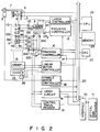
- Fig. 2 shows a disk apparatus. Grooves (record tracks) are spirally formed in a surface of optical disk (disk) 1. Optical disk 1 is rotated at, e.g., a constant speed by motor 2. Motor 2 is controlled by spindle motor controller 18.
- Optical disk 1 has a size of, e.g., 5.25 inches (about 13.3 cm) and is designed such that a metal coating layer consisting of tellurium or bismuth, i.e., a recording layer, is coated on a surface of a circular glass or plastic substrate in the form of a doughnut, and notched portions, i.e., reference position marks, are formed near the center of the metal coating layer.
- a metal coating layer consisting of tellurium or bismuth i.e., a recording layer
- data record area 1a and characteristic data record area 1b are formed on optical disk 1.
- Guide grooves are formed in the data record area 1a.
- characteristic data record area 1b is formed closer to the center of optical disk 1 than data record area 1a and includes no guide grooves and servo bytes.
- Control track C is to be recorded in characteristic data record area 1b in advance in the process of manufacturing optical disk 1.
- Three sets of identical characteristic data are formed on control track C per revolution in the form of bar code data in the circumferential direction.
- This characteristic data includes the characteristics (reflectivity) of a film of optical disk 1, the recording/reproducing power of a semiconductor laser, a format (the number of sectors per revolution), and the like. Above-mentioned continuity and discontinuity of pit strings and is radially recorded in the radial direction of optical disk 1.
- the recording position of control track C is defined by the distance from the center of optical disk 1 (radial position).
- control track C is recorded between a position 29.0 mm away from the center and a position 29.3 mm away from the center.
- CAV constant angular velocity
- CLV constant length velocity
- MCAV modified CAV
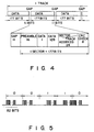
- control track C is constituted by three sectors. Each sector is constituted by a gap, a preamble, a sync signal, characteristic data, sector/track address data, CRC check data, and the like.
- One-bit data of control track C is designed as follows. As shown in Fig. 5, if 82 pits constituting a pit string are continuously formed in the first half of a given bit portion, "0" is determined. If they are formed in the second half, "1" is determined.
- one-bit data of control track C is designed as follows. As shown in Fig. 6, if a plurality of pit strings are present in 328 channel bits of the first half of a given bit portion, "0" is determined. If they are present in 328 channel bits of the second half, "1" is determined.
- Above-mentioned data record area 1a is divided into a plurality of sectors with reference to the reference marks. Variable length data are recorded on optical disk 1 over a plurality of blocks. 300,000 blocks are formed on 36,000 tracks on optical disk 1.
- Optical head 3 is fixed to drive coil 13 constituting a movable portion of a linear motor.
- Drive coil 13 is connected to linear motor controller 17.
- Linear motor position detector 26 is connected to linear motor controller 17. Upon detection of optical scale 25 arranged on optical head 3, linear motor position detector 26 outputs a position signal.
- a permanent magnet (not shown) is arranged on the stationary portion of the linear motor so that when drive coil 13 is excited by linear motor controller 17, optical head 3 is moved in the radial direction of optical disk 1.
- Objective lens 6 is held on optical head 3 by a wire or a leaf spring (not shown). Objective lens 6 is moved in the focusing direction (the direction of the optical axis of lens 6) by drive coil 5 and is moved in the tracking direction (the direction perpendicular to the optical axis of lens 6).
- a laser beam generated by semiconductor laser 9 driven by laser controller 14 is radiated on optical disk 1 through collimator lens 11a, half prism 11b, and objective lens 6.
- the laser beam reflected by optical disk 1 is guided to photodetector 8 through half prism 11b, condenser lens 10a, and cylindrical lens 10b.
- Photodetector 8 is constituted by four identical photodetector cells 8a, 8b, 8c, and 8d.
- An output signal from photodetector cell 8a of photodetector 8 is supplied to one terminal of each of adders 30a and 30c through amplifier 12a.
- An output signal from photodetector cell 8b is supplied to one terminal of each of adders 30b and 30d through amplifier 12b.
- An output signal from photodetector cell 8c is supplied to the other terminal of each of adders 30b and 30c through amplifier 12c.
- An output signal from photodetector cell 8d is supplied to the other terminal of each of adders 30a and 30d through amplifier 12d.
- An output signal from adder 30a is supplied to the inverting input terminal of differential amplifier OP1.
- An output signal from adder 30b is supplied to the non-inverting input terminal of differential amplifier OP1.
- differential amplifier OP1 supplies a track difference signal corresponding to a difference between the outputs from adders 30a and 30b to tracking controller 16.
- Tracking controller 16 generates a track drive signal in accordance with the track difference signal supplied from differential amplifier OP1.
- the track drive signal output from tracking control circuit 16 is supplied to drive coil 4 for driving objective lens 6 in the tracking direction.
- the track difference signal used by tracking controller 16 is supplied to linear motor controller 17.
- An output signal from adder 30c is supplied to the inverting input terminal of differential amplifier OP2.
- An output signal from adder 30d is supplied to the noninverting input terminal of differential amplifier OP2.
- differential amplifier OP2 supplies a signal associated with a focal point to focusing controller 15 in accordance with a difference between the outputs from adders 30c and 30d.
- An output signal from focusing controller 15 is supplied to focusing drive coil 5 to control a laser beam to be always radiated on optical disk 1 in an in-focus state.
- Such a signal is supplied to video circuit 19 to reproduce image data and address data (a track number, a sector number, and the like).
- the reproduction signal reproduced by video signal 19 is output to optical disk apparatus 71 as an external unit through interface 70.
- Control track reader 31 outputs a binary signal corresponding to recorded data of control track C in accordance with the output signals from adders 30a and 30b.
- control track C When control track C is to be accessed, the binary signal is output to CPU 23 (to be described later).
- CPU 23 moves optical head 3 from the innermost circumference of optical disk 1.
- CPU 23 determines that the position of optical head 3 corresponds to a portion near the center of control track C, and stops optical head 3.
- CPU 23 reads the characteristic data of control track C by checking the time interval between high level and low level of a binary signal supplied from a comparator (to be described later) of control track reader 30, and performs a control operation corresponding to the read characteristic data. That is, CPU 23 can perform control operations corresponding to various specifications (manufacturers) of optical disks 1.
- the disk apparatus of this embodiment further includes a D/A converter 22 for data communication among focusing controller 15, tracking controller 16, linear motor controller 17, and CPU 23.
- Tracking controller 16 moves objective lens 6 in accordance with a track jump signal supplied from CPU 23 through D/A converter 22 so as to move a laser beam by a distance corresponding to one track.
- Laser controller 14, focusing controller 15, tracking controller 16, linear motor controller 17, spindle motor controller 18, video circuit 19, and the like are controlled by CPU 23 through bus line 20.
- CPU 23 is designed to perform a predetermined operation in accordance with a program stored in memory 24.
- control track reader 31 is constituted by adder 31a, lower edge detector 31b, and binary value generator 31c.
- Lower edge detector 31b comprises amplifier 32 and an integrator constituted by diode D1 and capacitor C1.
- Binary value generator 31c comprises diodes D2 and D3, resistor R1, capacitor C2, and comparator 33.
- the integrator (D1, C1) serves to remove noise (n) from signal r shown in Fig. 7A.
- Adder 31a adds the output signals from adders 30a and 30b together so as to output reproduction signal r corresponding to the sum of detection signals from photodetector cells 8a to 8d.
- Lower edge detector 31b outputs a lower edge detection signal (a signal obtained by detecting a dark level peak of reproduction signal r ) l from adder 31a.
- comparator 33 compares lower edge detection signal l from lower edge detector 31b with delay signal d obtained by delaying lower edge detection signal l . If lower edge detection signal l > delay signal d , comparator 33 outputs a signal of "H" level. If lower edge signal l > delay signal d , comparator 33 outputs a signal of "L” level. With this operation, binary value generator 31c outputs binary signal t corresponding to the recorded data of control track C to CPU 23.
- lower edge detection signal l (see Fig. 7B) is detected from reproduction signal r shown in Fig. 7A, and signal l is converted into a binary value by comparing lower edge detection signal l with delay signal d obtained by delaying lower edge detection signal l , thereby obtaining binary signal t (see Fig. 7C).
- a reading operation for control track C in the above-described arrangement will be described below. Assume that a command for access to control track C is supplied from optical disk controller 7 to CPU 23. CPU 23 then controls linear motor controller 17 to move optical head 3 outward from the innermost circumference of optical disk 1.
- CPU 23 causes semiconductor laser 9 to emit a laser beam.
- the laser beam emitted from semiconductor laser 9 is radiated on optical disk 1 through collimator lens 11a, half prism 11b, and objective lens 6.
- the laser beam reflected by optical disk 1 is guided to photodetector 8 through half prism 11b, condenser lens 10a, and cylindrical lens 10b.
- An output signal from photodetector cell 8a of photodetector 8 is supplied to one terminal of each of adders 30a and 30c through amplifier 12a.
- An output signal from photodetector cell 8b is supplied to one terminal of each of adders 30b and 30d through amplifier 12b.
- An output signal from photodetector cell 8c is supplied to the other terminal of each of adders 30b and 30c through amplifier 12c.
- An output signal from photodetector cell 8d is supplied to the other terminal of each of adders 30a and 30d through amplifier 12d.
- Adder 31a then outputs reproduction signal r (shown in Fig. 7A) corresponding to the sum of the detection signals from photodetector cells 8a to 8d to lower edge detector 31b.
- Lower edge detector 31b detects the lower edge of reproduction signal r from adder 31a and outputs lower edge detection signal l (indicated by a solid curve in Fig. 7B) to binary value generator 31c.
- comparator 33 compares lower edge detection signal l from lower edge detector 31b with delay signal d (indicated by a dotted curve in Fig. 7B) obtained by delaying lower edge detection signal l . If lower edge detection signal l > delay signal d , comparator 33 outputs a signal of "H" level. If lower edge detection signal l ⁇ delay signal d , comparator 33 outputs a signal of "L” level. With this operation, binary value generator 31c outputs binary signal t (see Fig. 7C) corresponding to the recorded data of control track C to CPU 23.
- CPU 23 reads the characteristic data of control track C by checking the time interval between high level and low level of binary signal t supplied from comparator 33 in control track reader 31, and performs a control operation corresponding to the read characteristic data. That is, CPU 23 performs control operations corresponding to various specifications (manufacturers) of different optical disks 1.
- control is performed in accordance with specifications corresponding to the characteristics (reflectivity) of optical disk 1, the recording/reproducing power of a semiconductor laser, a format (the number of sectors per revolution), and the like.
- a dark level peak of a reproduction signal is detected, and tha peak signal is compared with a delay signal obtained delaying the peak signal so as to convert the reproduction signal into a binary value, thereby reproducing an accurate binary signal.
- the characteristic data of a control track in a characteristic data record area where no guide grooves and servo bytes are present can be read without being influenced by eccentricity and the like. Even if an eccentricity amount varies depending on a type of optical disk, the characteristic data of a control track can be reliably read.
- Fig. 1 shows an arrangement of an optical disk apparatus to which a binary signal detector according to the present invention is applied.
- the present invention can be widely applied to cases wherein binary data is to be accurately detected from an analog signal having level variations without being influenced by the level variations.
- Figs. 1A and 1B show basic arrangements of such a general-purpose binary signal detector.
- a binary signal detector shown in Fig. 1A comprises: delay circuit 200 for delaying analog signal s (corresponding to signal r in Fig. 7A) having level variations by a predetermined period of time so as to output delayed analog signal d (Fig. 7B) which is delayed from a change in the level of analog signal s and changes in proportion to the level change of analog signal s ; amplifier 100 for amplifying analog signal s at amplification k > 1, and providing analog reference signal l having a larger amplitude than delayed analog signal d ; and comparator 33 for comparing the level of analog reference signal l with that of delayed analog signal d , and generating binary output t (Fig. 7C) having a logic level corresponding to the binary data when the signal level of analog reference signal l is different from that of delayed analog signal d (e.g., l > d).
- a binary signal detector shown in Fig. 1B comprises: delay circuit 200 for delaying analog signal s having level variations by a predetermined period of time so as to output delayed analog signal d* which is delayed from a change in the level of analog signal s and changes in proportion to the level change of analog signal s ; amplifier 101 for amplifying delayed analog signal d* at amplification k ⁇ 1 (i.e., attenuating), and providing delayed analog signal d having a smaller amplitude than delayed analog signal d*; and comparator 33 for comparing the level of analog signal s with that of delayed analog signal d , and generating binary output t having a logic level corresponding to the binary data when the signal level of analog signal s is different from that of delayed analog signal d (e.g., s > d).
- delay circuit 200 for delaying analog signal s having level variations by a predetermined period of time so as to output delayed analog signal d* which is delayed from a change in the level of analog signal s and changes in proportion to
- a disk apparatus which can accurately read characteristic data in a characteristic data record area where no guide grooves and servo bytes are present.
Landscapes
- Optical Recording Or Reproduction (AREA)
- Signal Processing For Digital Recording And Reproducing (AREA)
- Optical Record Carriers And Manufacture Thereof (AREA)
Claims (7)
- Wiedergabegerät zum Wiedergeben von Information von einem optischen Aufzeichnungsmedium (1) gemäß darauf aufgezeichneten Daten, die für Charakteristiken des optischen Aufzeichnungsmediums (1) repräsentativ sind, mit:
einer Einrichtung (3) zum Einstrahlen eines einfallenden Lichtstrahles auf das optische Aufzeichnungsmedium (1) und zum Erzeugen eines analogen Signales (r) entsprechend den Daten durch Empfangen eines reflektierten Lichtstrahles von dem optischen Aufzeichnungsmedium,
dadurch gekennzeichnet, daß das Gerät außerdem umfaßt:
eine Einrichtung (31b) zum Durchführen einer unteren Randerfassung auf dem analogen Signal (r) und zum Ausgeben eines unteren Randerfassungssignales (s) im wesentlichen entsprechend dem unteren Rand des analogen Signales (r),
eine Einrichtung (200) zum Verzögern des unteren Randerfassungssignales (s) um eine vorbestimmte Zeitdauer, um ein verzögertes analoges Signal (d) auszugeben,
eine Einrichtung (100 oder 101) zum Liefern eines analogen Bezugssignales (ℓ), das sich proportional zu der Pegeländerung des unteren Randerfassungssignales (s) ändert und das eine größere Amplitude hat als das verzögerte analoge Signal (d),
eine Einrichtung (33) zum Vergleichen des Pegels des analogen Bezugssignales (ℓ) mit demjenigen des verzögerten analogen Signales (d) und, wenn der Signalpegel des analogen Bezugssignales (ℓ) verschieden ist von demjenigen des verzögerten analogen Signales (d), zum Erzeugen eines binären Ausgangssignales mit einem binären logischen Pegel, der anzeigt, welches Signal aus dem analogen Bezugssignal (ℓ) oder dem verzögerten analogen Signal (d) den höheren Pegel hat, und
eine Einrichtung (23) zum Wiedergeben der Information (Fig. 4) von dem optischen Aufzeichnungsmedium (1) gemäß den von dem erzeugten binären Ausgangssignal (t) wiedergegebenen Daten. - Gerät nach Anspruch 1, gekennzeichnet durch weiterhin eine Einrichtung (31a) zum Kombinieren einer Vielzahl von photoelektrischen Umsetzungssignalen (30a, 30b) entsprechend auf der optischen Platte (1) aufgezeichneten Pit-Daten und zum Ausgeben des analogen Signales (r).
- Gerät nach Anspruch 1, dadurch gekennzeichnet, daß(a) die Liefereinrichtung (100 oder 101) eine erste Einrichtung (31b, R1) zum Ausgeben des analogen Bezugssignales (ℓ) proportional zu dem analogen Signal (r) umfaßt,(b) die Verzögerungseinrichtung (200) umfaßt:
eine Einrichtung (31) zum Integrieren des analogen Signales (r) als eine Funktion der Zeit, um das untere Randdetektionssignal (s) auszugeben, und
eine zweite Einrichtung (R1, D2, D3, C2) zum Erzeugen des verzögerten analogen Signales (d), das proportional zu dem unteren Randdetektionssignal (s) ist, sich im Pegel mit einer Verzögerung von der Signalpegeländerung des analogen Bezugssignales (ℓ) ändert und das eine kleinere Amplitude als das analoge Bezugssignal (ℓ) hat, und(c) die Vergleichereinrichtung (33) das binäre Ausgangssignal (t) erzeugt, das auf einen ersten logischen Pegel eingestellt ist, wenn der Pegel des analogen Bezugssignales (ℓ) höher als derjenige des verzögerten analogen Signales (d) ist, und das auf einen zweiten logischen Pegel, der vom ersten logischen Pegel verschieden ist, eingestellt ist, wenn der Pegel des analogen Bezugssignales (ℓ) niedriger als das verzögerte analoge Signal (d) ist. - Gerät nach Anspruch 1, dadurch gekennzeichnet, daß die Verzögerungseinrichtung (200) umfaßt:
eine Einrichtung (31b) zum Integrieren des analogen Signales (r) als eine Funktion der Zeit, um das untere Randdetektionssignal (s) auszugeben, und
eine Vergleichssignaleinrichtung (R1, D2, D3, C2) zum Erzeugen des verzögerten analogen Signales (d), das proportional zu dem unteren Randdetektionssignal (s) ist, sich im Pegel mit einer Verzögerung von einer Signalpegeländerung des unteren Randdetektionssignales (s) ändert und das eine kleinere Amplitude als das untere Randdetektionssignal (s) hat, und
die Vergleichereinrichtung (33) eine Einrichtung zum Vergleichen eines Signalpegels des unteren Randdetektionssignales (s) mit demjenigen des verzögerten analogen Signales (d) und zum Erzeugen des binären Ausgangssignales (t) hat, das auf einen ersten logischen Pegel eingestellt ist, wenn der Pegel des unteren Randdetektionssignales höher als derjenige des verzögerten analogen Signales (d) ist, und das auf einen zweiten logischen Pegel eingestellt ist, wenn der Pegel des unteren Randdetektionssignales niedriger als derjenige des verzögerten analogen Signales (d) ist. - Gerät nach Anspruch 3, dadurch gekennzeichnet, daß die zweite Einrichtung (R1, D2, D3, C2) umfaßt:
antiparallel gekoppelte Dioden (D1, D2), die zwischen einen Signalknoten des analogen Bezugssignales (ℓ) und einen Signalknoten des verzögerten analogen Signales (d) eingefügt sind, und
einen Kondensator (C2), der zwischen den Signalknoten des verzögerten analogen Signales (d) und eine Schaltungsmasse eingefügt ist. - Gerät nach Anspruch 4, dadurch gekennzeichnet, daß die Vergleichssignaleinrichtung (R1, D2, D3, C2) umfaßt:
antiparallel gekoppelte Dioden (D1, D2), die zwischen einen Signalknoten des unteren Randdetektionssignales (s) und einen Signalknoten des verzögerten analogen Signales (d) eingefügt sind, und
einen Kondensator (C2), der zwischen den Signalknoten des verzögerten analogen Signales (d) und eine Masseschaltung eingefügt ist. - Gerät nach einem der Ansprüche 3 bis 6, dadurch gekennzeichnet, daß die Integriereinrichtung (31) umfaßt:
einen Pufferverstärker (32) zum Empfangen des analogen Signales (r) an einer Eingangsseite des Pufferverstärkers (32), und
einen Kondensator (C1), der zwischen die Eingangsseite des Pufferverstärkers (32) und eine Schaltungsmasse eingefügt ist.
Applications Claiming Priority (2)
| Application Number | Priority Date | Filing Date | Title |
|---|---|---|---|
| JP252166/89 | 1989-09-29 | ||
| JP1252166A JP2752190B2 (ja) | 1989-09-29 | 1989-09-29 | ディスク装置 |
Publications (3)
| Publication Number | Publication Date |
|---|---|
| EP0420206A2 EP0420206A2 (de) | 1991-04-03 |
| EP0420206A3 EP0420206A3 (en) | 1992-01-15 |
| EP0420206B1 true EP0420206B1 (de) | 1995-07-19 |
Family
ID=17233408
Family Applications (1)
| Application Number | Title | Priority Date | Filing Date |
|---|---|---|---|
| EP90118495A Expired - Lifetime EP0420206B1 (de) | 1989-09-29 | 1990-09-26 | Detektor für binäre Signale |
Country Status (4)
| Country | Link |
|---|---|
| US (1) | US5126741A (de) |
| EP (1) | EP0420206B1 (de) |
| JP (1) | JP2752190B2 (de) |
| DE (1) | DE69020996T2 (de) |
Families Citing this family (9)
| Publication number | Priority date | Publication date | Assignee | Title |
|---|---|---|---|---|
| DE69535603T2 (de) | 1994-11-17 | 2008-02-21 | Matsushita Electric Industrial Co., Ltd., Kadoma | Optische Platte, Verfahren zur Herstellung einer optischen Platte und Wiedergabegerät |
| USRE39653E1 (en) | 1994-11-17 | 2007-05-22 | Matsushita Electric Industrial Co., Ltd. | Mark forming apparatus, method of forming laser mark on optical disk, reproducing apparatus, optical disk and method of producing optical disk |
| US5586755A (en) * | 1995-02-13 | 1996-12-24 | Xerox Corporation | Misfeed detector for a stack of different weight sheets |
| US6107637A (en) * | 1997-08-11 | 2000-08-22 | Hitachi, Ltd. | Electron beam exposure or system inspection or measurement apparatus and its method and height detection apparatus |
| DK1190419T3 (en) * | 2000-02-23 | 2015-12-07 | Koninkl Philips Nv | Overwriting sight data storage medium |
| US6592985B2 (en) * | 2000-09-20 | 2003-07-15 | Camco International (Uk) Limited | Polycrystalline diamond partially depleted of catalyzing material |
| JP2003296943A (ja) * | 2002-03-29 | 2003-10-17 | Sony Corp | 光ディスク、光ディスク再生装置及び再生方法、並びに光ディスクの製造方法 |
| JP3916546B2 (ja) * | 2002-10-24 | 2007-05-16 | パイオニア株式会社 | 再生専用の記録媒体 |
| JP2006155802A (ja) * | 2004-11-30 | 2006-06-15 | Toshiba Corp | 情報記憶媒体、スタンパー、管理情報記録装置、ディスク装置、管理情報再生方法 |
Family Cites Families (4)
| Publication number | Priority date | Publication date | Assignee | Title |
|---|---|---|---|---|
| US3737808A (en) * | 1971-12-29 | 1973-06-05 | Honeywell Inf Systems | Pulse shaping network |
| BE793746A (fr) * | 1972-01-11 | 1973-07-09 | Sercel Rech Const Elect | Amplificateur d'echantillons de signaux analogiques avec reglage de gain automatique |
| US4167028A (en) * | 1978-04-13 | 1979-09-04 | Recortec, Inc. | Method and an apparatus for time signal encoding/decoding |
| US4961182A (en) * | 1987-07-01 | 1990-10-02 | Hitachi, Ltd. | Information retrieving system with level clamping |
-
1989
- 1989-09-29 JP JP1252166A patent/JP2752190B2/ja not_active Expired - Lifetime
-
1990
- 1990-09-24 US US07/586,986 patent/US5126741A/en not_active Expired - Lifetime
- 1990-09-26 EP EP90118495A patent/EP0420206B1/de not_active Expired - Lifetime
- 1990-09-26 DE DE69020996T patent/DE69020996T2/de not_active Expired - Fee Related
Also Published As
| Publication number | Publication date |
|---|---|
| DE69020996T2 (de) | 1995-11-23 |
| JP2752190B2 (ja) | 1998-05-18 |
| US5126741A (en) | 1992-06-30 |
| JPH03116441A (ja) | 1991-05-17 |
| EP0420206A3 (en) | 1992-01-15 |
| DE69020996D1 (de) | 1995-08-24 |
| EP0420206A2 (de) | 1991-04-03 |
Similar Documents
| Publication | Publication Date | Title |
|---|---|---|
| JP2799002B2 (ja) | ディスク装置 | |
| JP3039099B2 (ja) | 光ディスク記録装置およびその方法 | |
| JP2732591B2 (ja) | 記録媒体処理装置 | |
| JP2635610B2 (ja) | ディスク装置 | |
| KR100255191B1 (ko) | 광 디스크 재생장치에서 종류 검출을 위한 디스크와그 종류 검출방법 | |
| US6842414B1 (en) | Apparatus and method for compensating tilt of optical disc | |
| US5724325A (en) | Method for reducing lead in time in an optical disk recording or reproducing apparatus capable of processing data for multiple types of disks | |
| EP0363022B1 (de) | Spursignal in einem optischen Informationsaufzeichnungs- und/oder -wiedergabegerät | |
| US5155722A (en) | Recording/reproducing apparatus | |
| US5126741A (en) | Reproduction apparatus having circuit for accurately detecting a binary waveform from a varying level analog signal | |
| US4918680A (en) | Focus-servo correction utilizing storage of detected focus errors | |
| KR100464413B1 (ko) | 광기록매체의 종류 판별방법 및 장치 | |
| US5128920A (en) | Optical disk apparatus with a laser beam controllable in accordance with a specification area on a disk | |
| US5058092A (en) | Method for accessing a control track by positioning an optical head at the center of the control track | |
| JP2713999B2 (ja) | ディスク装置 | |
| US5210731A (en) | Information processing apparatus with missing pulse detection and correction | |
| JP2703269B2 (ja) | 情報記録再生装置 | |
| JPH0453033A (ja) | 光磁気記録再生装置 | |
| JP2695834B2 (ja) | 情報再生装置 | |
| US6747925B2 (en) | Method and system for generating a center error signal in an optical storage system | |
| JPH01276433A (ja) | ディスク装置 | |
| JPH05274694A (ja) | ディスク装置 | |
| JPH056550A (ja) | デイスク装置 | |
| JPH05274691A (ja) | ディスク装置 | |
| JP3017738B2 (ja) | 光ディスク装置 |
Legal Events
| Date | Code | Title | Description |
|---|---|---|---|
| PUAI | Public reference made under article 153(3) epc to a published international application that has entered the european phase |
Free format text: ORIGINAL CODE: 0009012 |
|
| 17P | Request for examination filed |
Effective date: 19901023 |
|
| AK | Designated contracting states |
Kind code of ref document: A2 Designated state(s): DE FR GB NL |
|
| PUAL | Search report despatched |
Free format text: ORIGINAL CODE: 0009013 |
|
| AK | Designated contracting states |
Kind code of ref document: A3 Designated state(s): DE FR GB NL |
|
| 17Q | First examination report despatched |
Effective date: 19940318 |
|
| GRAA | (expected) grant |
Free format text: ORIGINAL CODE: 0009210 |
|
| AK | Designated contracting states |
Kind code of ref document: B1 Designated state(s): DE FR GB NL |
|
| REF | Corresponds to: |
Ref document number: 69020996 Country of ref document: DE Date of ref document: 19950824 |
|
| ET | Fr: translation filed | ||
| PLBE | No opposition filed within time limit |
Free format text: ORIGINAL CODE: 0009261 |
|
| STAA | Information on the status of an ep patent application or granted ep patent |
Free format text: STATUS: NO OPPOSITION FILED WITHIN TIME LIMIT |
|
| 26N | No opposition filed | ||
| PGFP | Annual fee paid to national office [announced via postgrant information from national office to epo] |
Ref country code: DE Payment date: 19961004 Year of fee payment: 7 |
|
| PGFP | Annual fee paid to national office [announced via postgrant information from national office to epo] |
Ref country code: FR Payment date: 19970909 Year of fee payment: 8 |
|
| PGFP | Annual fee paid to national office [announced via postgrant information from national office to epo] |
Ref country code: GB Payment date: 19970917 Year of fee payment: 8 |
|
| PGFP | Annual fee paid to national office [announced via postgrant information from national office to epo] |
Ref country code: NL Payment date: 19970929 Year of fee payment: 8 |
|
| PG25 | Lapsed in a contracting state [announced via postgrant information from national office to epo] |
Ref country code: DE Free format text: LAPSE BECAUSE OF NON-PAYMENT OF DUE FEES Effective date: 19980603 |
|
| PG25 | Lapsed in a contracting state [announced via postgrant information from national office to epo] |
Ref country code: GB Free format text: LAPSE BECAUSE OF NON-PAYMENT OF DUE FEES Effective date: 19980926 |
|
| PG25 | Lapsed in a contracting state [announced via postgrant information from national office to epo] |
Ref country code: NL Free format text: LAPSE BECAUSE OF NON-PAYMENT OF DUE FEES Effective date: 19990401 |
|
| GBPC | Gb: european patent ceased through non-payment of renewal fee |
Effective date: 19980926 |
|
| PG25 | Lapsed in a contracting state [announced via postgrant information from national office to epo] |
Ref country code: FR Free format text: LAPSE BECAUSE OF NON-PAYMENT OF DUE FEES Effective date: 19990531 |
|
| NLV4 | Nl: lapsed or anulled due to non-payment of the annual fee |
Effective date: 19990401 |
|
| REG | Reference to a national code |
Ref country code: FR Ref legal event code: ST |