EP0420477A2 - Circuit décodeur pour une prom - Google Patents
Circuit décodeur pour une prom Download PDFInfo
- Publication number
- EP0420477A2 EP0420477A2 EP90310208A EP90310208A EP0420477A2 EP 0420477 A2 EP0420477 A2 EP 0420477A2 EP 90310208 A EP90310208 A EP 90310208A EP 90310208 A EP90310208 A EP 90310208A EP 0420477 A2 EP0420477 A2 EP 0420477A2
- Authority
- EP
- European Patent Office
- Prior art keywords
- decoder
- transistors
- circuit
- power supply
- current supply
- Prior art date
- Legal status (The legal status is an assumption and is not a legal conclusion. Google has not performed a legal analysis and makes no representation as to the accuracy of the status listed.)
- Granted
Links
Images


Classifications
-
- G—PHYSICS
- G11—INFORMATION STORAGE
- G11C—STATIC STORES
- G11C16/00—Erasable programmable read-only memories
- G11C16/02—Erasable programmable read-only memories electrically programmable
- G11C16/06—Auxiliary circuits, e.g. for writing into memory
-
- H—ELECTRICITY
- H03—ELECTRONIC CIRCUITRY
- H03K—PULSE TECHNIQUE
- H03K19/00—Logic circuits, i.e. having at least two inputs acting on one output; Inverting circuits
- H03K19/003—Modifications for increasing the reliability for protection
- H03K19/00346—Modifications for eliminating interference or parasitic voltages or currents
- H03K19/00361—Modifications for eliminating interference or parasitic voltages or currents in field effect transistor circuits
-
- G—PHYSICS
- G11—INFORMATION STORAGE
- G11C—STATIC STORES
- G11C16/00—Erasable programmable read-only memories
- G11C16/02—Erasable programmable read-only memories electrically programmable
- G11C16/06—Auxiliary circuits, e.g. for writing into memory
- G11C16/08—Address circuits; Decoders; Word-line control circuits
-
- G—PHYSICS
- G11—INFORMATION STORAGE
- G11C—STATIC STORES
- G11C17/00—Read-only memories programmable only once; Semi-permanent stores, e.g. manually-replaceable information cards
- G11C17/14—Read-only memories programmable only once; Semi-permanent stores, e.g. manually-replaceable information cards in which contents are determined by selectively establishing, breaking or modifying connecting links by permanently altering the state of coupling elements, e.g. PROM
- G11C17/18—Auxiliary circuits, e.g. for writing into memory
-
- G—PHYSICS
- G11—INFORMATION STORAGE
- G11C—STATIC STORES
- G11C8/00—Arrangements for selecting an address in a digital store
- G11C8/10—Decoders
Definitions
- the present invention relates to a decoder circuit, more particularly, to a decoder circuit of a programmable read only memory (which includes, for example, an erasable programmable read only memory: EPROM or a one time programmable read only memory: OTPROM) having a plurality of floating gate avalanche injection MOS (FAMOS) transistors as memory cells.
- a programmable read only memory which includes, for example, an erasable programmable read only memory: EPROM or a one time programmable read only memory: OTPROM
- FMOS floating gate avalanche injection MOS
- an EPROM comprises a cell matrix portion (memory cell array) formed by a plurality of FAMOS transistors as memory elements (memory cells), bit lines and word lines for selecting a specific memory cell, and decoder circuit for driving them.
- a power supply voltage is brought to a low voltage (for example, 5 volts) at the time of reading out (reading-out time), a memory cell corresponding to an address signal (of which the voltage value is, for example, at 0 volts or 5 volts) is selected and data is output therefrom.
- the power supply voltage is brought to a high voltage (for example, 12.5 volts), and the writing operation is carried out thereby.
- a high voltage for example, 12.5 volts
- the memory cell of a FAMOS transistor is written by using the high voltage of 12.5 volts.
- a decoder circuit of an EPROM comprising a NAND gate circuit including a load transistor and a plurality of decoder transistors and a CMOS inverter circuit receiving an output of the NAND gate circuit is proposed (which is, for example, disclosed in Japanese Unexamined Patent Publication No. 61-45496).
- a booster circuit for a writing operation is not provided between the NAND gate circuit and the CMOS inverter circuit, as the NAND gate circuit comprises the load transistor used as a constant current source and is supplied with a power supply voltage changeable between a high voltage Vpp (12.5 volts) and a low voltage Vcc (5 volts).
- an output of the NAND gate circuit of this decoder circuit is already at a high voltage level Vpp by receiving the high voltage Vpp, and thus the booster circuit for boosting an output (which is at a low voltage level Vcc) of a conventional NAND gate circuit to a high voltage level Vpp is not required. Therefore, this decoder circuit (for example, shown in JPP'496) is preferable for a large scale integration of an EPROM, as the booster circuit is not required.
- the NAND gate circuit a plurality of parasitic capacitors are formed at connection points among the decoder transistors. Note, the ability to supply the current of the load transistor is not large, and thus in the case of a plurality of parasitic capacitors being charged, a potential drop at the output of the NAND gate circuit is caused and an erroneous operation of the EPROM may be caused (which is described in later in detail).
- a decoder circuit used in a programmable read only memory, comprising: a first high potential power supply line for supplying a voltage changeable between a high voltage and a low voltage; a low potential power supply line; a load unit connected between the first high potential power supply line and a decoded output terminal; a plurality of decoder transistors, connected in series between the decoded output terminal and the low potential power supply line, and gates of the decoder transistors being supplied with input signals; a current supply unit, connected to at least one of a plurality of connection points of the decoder transistors, for supplying a current to the at least one of the connection points, when at least one of the decoder transistors except the nearest decoder transistor of the decoded output terminal is switched OFF.
- the current supply unit may be connected to one point of the plurality of connection points.
- the current supply unit may be connected to the nearest connection point of the decoded output terminal in the connection points.
- the decoder transistors may be formed by first conduction type MOS transistors; and the current supply unit may comprise a plurality of current supply transistors formed by second conduction type MOS transistors opposite to the first conduction type, sources of the current supply transistors may be connected to a second high potential power supply line for supplying the low voltage, drains of the current supply transistors may be connected to at least one of the connection points, and gates of the current supply transistors may be supplied with the input signals except the nearest input signal received by the nearest decoder transistor of the decoded output terminal.
- All of the drains of the current supply transistors may be commonly connected to one point of the plurality of connection points. All of the drains of the current supply transistors may be commonly connected to the nearest connection point of the decoded output terminal in the connection points. Each of the drains of the current supply transistors may be respectively connected to corresponding connection points, and when a specific decoder transitor is switched OFF, the connection points from the specific decoder transistor to the decoded output terminal may be supplied with a current by the current supply transistors in accordance with the input signals except the nearest input signal.
- the corresponding connection points may be determined as drains of the decoder transistors whose gates are supplied with the same input signals except the nearest input signal of the decoded output terminal supplied to the gates of the current supply transistors.
- the load unit may be used as a constant current source.
- the load unit may be formed by a depletion mode n-channel MOS transistor.
- a programmable read only memory comprising: a cell matrix portion, having a plurality of word lines, a plurality of bit lines, and a plurality of memory cells connected between each of the word lines and each of the bit lines; a column decoder, connected to the cell matrix portion through the bit lines, for selecting one of the bit lines in accordance with address signals; a row decoder, connected to the cell matrix portion through the word lines, for selecting one of the word lines in accordance with address signals; a sense amplifier, connected to the cell matrix portion through the bit lines, for sensing a content of the selected memory cell; a data input buffer and program control circuit, connected to the cell matrix portion through the bit lines, for storing write data and supplying the write date to the cell matrix portion; an output enable and chip enable circuit, connected to the data input buffer and program control circuit, the column decoder, the row decoder, and the sense amplifier, for controlling them; and a high potential power supply unit, for selectively supplying a
- a current supply unit connected to at least one of a plurality of connection points of the decoder transistors, for supplying a current to the at least one of the connection points, when at least one of the decoder transistors except the nearest decoder transistor of the decoded output terminal is switched OFF.
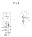
- Figure 1 is a circuit diagram illustrating a conventional decoder circuit according to the prior art.
- a reference 1 denotes a CMOS inverter circuit
- 3 denotes an output of the decoder circuit, or a word line output.
- a reference 4 denotes a power supply line changeable between a high voltage (Vpp) and a low voltage (Vcc)
- 5 denotes a ground line
- 6 denotes a NAND gate circuit.
- the decoder circuit comprises the NAND gate circuit 6 and the CMOS inverter circuit 1.
- the NAND gate circuit 6 comprises a depletion mode n-channel MOS transistor (load transistor) D2, and a plurality of enhancement mode n-channel MOS transistors (decoder transistors) Q21 ⁇ Q24.
- the CMOS inverter circuit 1 comprises an enhancement mode p-channel MO transistor Q26 and an enhancement mode n-channel MOS transistors Q27.
- the load transistor D2 is connected between the high potential power supply line 4 and a decoded output terminal X, and the decoder transistors Q21 ⁇ Q24 are connected in series between the decoded output terminal X and the low potential power supply line 5.
- Gates of the decoder transistors Q21 ⁇ Q24 are supplied with input signals a0 ⁇ a3.
- the input signals a0 ⁇ a3 may be address signals or predecoded address signals.
- references P1 ⁇ P3 denote connection points (interconnection points) among the decoder transistors Q21 ⁇ Q24, and C1 ⁇ C3 denote parasitic capacitors which are parasitically formed at the connection points P1 ⁇ P3.
- the decoded output terminal X which is an output of the NAND gate circuit 6, is connected to an input of the CMOS inverter circuit 1.
- the load transistor D2 of the NAND gate circuit 6 is a depletion mode transistor, and is used as a constant current source.
- a power supply voltage of the NAND gate circuit 6 and the CMOS inverter circuit 1 is to a high voltage Vpp (12.5 volts) at the writing time, and is changed to a low voltage Vcc (5 volts) at the reading-out time.
- the semiconductor memory device EPROM
- the number of address signals, or the number of input bits are increased in accordance with enlarging the capacity of the memory, so that the number of transistors constituting the NAND gate circuit 6 becomes large. Therefore, in the conventional decoder circuit, it is found that an erroneous operation of the decoder circuit is caused by the parasitic capacitors C1 ⁇ C3 which are indicated by a broken line in Fig. 1. This erroneous operation of the decoder circuit will be explained with reference to Fig. 2.
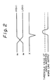
- Figure 2 is a diagram illustrating waveforms for explaining an erroneous operation in the conventional decoder circuit shown in Fig. 1.
- references a0 and a3 denote voltage levels of input signals
- a reference X denotes an input voltage level of the CMOS inverter ciruit 1.
- a power supply voltage is determined at 5 volts at the reading-out time.
- the decoded output terminal X (X-point) is at a high level "H", and an output of the CMOS inverter circuit 1, which is a word line output, is at a low level "L”.
- the decoder transistor Q21 is maintained at the switched OFF state, and the decoder transistors Q22 ⁇ Q24 are maintained at the switched ON states, and thus electric charges of the parasitic capacitors C1 ⁇ C3 are discharged to ground GND (low potential power supply line 5).
- the output of the CMOS inverter circuit 1 which is a word line output, is changed from a low level "L” to a high level "H", and a select level signal for selecting a memory cell is instantaneously output by the momentary potential drop. Consequently, a word line, which is not originally required to be selected, is selected as an error by the above described momentary potential drop, that is, an erroneous operation is caused in the EPROM by the parasitic capacitors C1 ⁇ C3 formed at the connection points P1 ⁇ P3 among the decoder transistors Q21 ⁇ Q24.
- Figure 3 is a circuit diagram iIlustrating a first embodiment of a decoder circuit according to the present invention.
- a first embodiment of a decoder circuit (word line decoder circuit formed in a row decoder 104 in Fig. 5) in an EPROM will be explained with reference to Fig. 3.
- the decoder circuit of the present invention is not only applied to an EPROM (erasable programmable read only memory), but also applied to an OTPROM (one time programmable read only memory).
- a reference 1 denotes a CMOS inverter circuit
- 2 denotes a current supply circuit
- 3 denotes an output of the decoder circuit, or a word line output.
- a reference 4 denotes a power supply line changeable between a high voltage (Vpp) and a low voltage (Vcc)
- 5 denotes a ground line
- 6 denotes a NAND gate circuit.
- the power supply line 4 is brought to a high voltage Vpp (12.5 volts) at the writing time, and is brought to a low voltage Vcc (5 volts) at the reading-out time.
- the decoder circuit comprises the NAND gate circuit 6, the CMOS inverter circuit 1, and the current supply circuit 2.
- the NAND gate circuit 6 comprises a depletion mode n-channel MOS transistor (load transistor) D1, and a plurality of enhancement mode n-channel MOS transistors (decoder transistors) Q1 ⁇ Q4.
- the CMOS inverter circuit 1 comprises an enhancement mode p-channel MOS transistor Q6 and an enhancement mode n-channel MOS transistors Q7.
- the current supply circuit 2 comprises a plurality of enhancement mode p-channel MOS transistors (current supply transistors) Q8 ⁇ Q10.
- the load transistor D1 is connected between the high potential power supply line 4 and a decoded output terminal X, and the decoder transistors Q1 ⁇ Q4 are connected in series between the decoded output terminal X and the low potential power supply line 5.
- Gates of the decoder transistors Q1 ⁇ Q4 are supplied with input signals a0 ⁇ a3, and further, gates of the power supply transistors Q8 ⁇ Q10 are supplied with the input signals a1 ⁇ a3. Namely, the decoder transistor Q2 and the power supply transistor Q8 are controlled by the input signal a1, the decoder transistor Q3 and the power supply transistor Q9 are controlled by the input signal a2, and the decoder transistor Q4 and the power supply transistor Q10 are controlled by the input signal a3.
- sources of the power supply transistors Q8 ⁇ Q10 are connected to a power supply line 7 for only supplying a low voltage Vcc (5 volts), and drains of the power supply transistors Q8 ⁇ Q10 are connected to a connection point P1.
- the input signals a0 ⁇ a3 are address signals, or the signals generated by predecoding the address signals. Further, voltage levels of the input signals a0 ⁇ a3 supplied to the gates of the decoder transistors Q1 ⁇ Q4 are determined at high levels "H" (5 volts) or low levels "L” (0 volts).
- references P1 ⁇ P3 denote connection points (interconnection points) among the decoder transistors Q1 ⁇ Q4, and C1 ⁇ C3 denote parasitic capacitors which are parasitically formed at the connection points P1 ⁇ P3.
- the decoded output terminal X which is an output of the NAND gate circuit 6, is connected to an input of the CMOS inverter circuit 1.
- a configuration of the EPROM including the decoder circuit will be explained after with reference to Fig. 5.
- the load transistor D of the NAND gate circuit 6 is a depletion mode transistor, and is used as a constant current source.
- a power supply voltage of the NAND gate circuit 6 and the CMOS inverter circuit 1 is set to a high voltage Vpp (12.5 volts) at the writing time, and is changed to a low voltage Vcc (5 volts) at the reading-out time.
- the decoder transistor Q1 is maintained at the switched OFF state, and the decoder transistors Q2 ⁇ Q4 are maintained at the switched ON states, and thus electric charges of the parasitic capacitors C1 ⁇ C3 are discharged to ground GND (low potential power supply line 5).
- the current supply circuit 2 does not supply a current to the connection point P1, since all of the current supply transistors Q8 ⁇ Q10 are switched OFF.
- a charge operation of the parasitic capacitors C1 ⁇ C3 is not only carried out by the load transistor D1, but also by the current supply transistors Q8 ⁇ Q10 (current supply circuit 2). Therefore, a potential drop of the decoded output terminal X (X-point), or an instantaneous drop of an output voltage of the CMOS inverter circuit 1 can be reduced, so that a nonselected word line being instantaneously selected in an erroneous operation is avoided.
- the decoder transistors Q2 and Q4 are switched OFF.
- the current supply transistors Q8 and Q10 are switched ON, and the parasitic capacitor C1 is charged by currents of the load transistor D1 and the current supply transistors Q8 and Q10 (current supply circuit 2), so that an instantaneous potential drop of the X-point can be avoided in the same manner as described above.
- voltages of the high power supply lines 4 are at high voltages Vpp (12.5 volts), that is, power supply voltages of the NAND gate circuit 6 and the CMOS inverter circuit 1 are brought to high voltages Vpp (12.5 volts). Therefore, a logical threshold value of the CMO inverter circuit 1 is brought to about Vpp/2 (volts), that is, the logical threshold value of the CMOS inverter circuit 1 is higher than the reading-out time, even if a voltage of the X-point is instantaneously dropped by the charge operation of the parasitic capacitors C1 ⁇ C3, so that an erroneous operation is not caused.
- the power supply voltage is at the high voltage Vpp (12.5 volts) and. the low voltage Vcc (5 volts) is applied to the current supply transistors Q8 ⁇ Q10, for example, when the input signals a0 ⁇ a3 are at levels "H", “L”, “L”, “L”, the current supply transistor Q8 is switched ON, and the connection point P1 which is a source of the transistor Q1 is at about 5 volts.
- the transistor Q1 is switched OFF by a gate-source voltage V gs having no potential difference, as the input signal a0 is at 5 volts.
- the output of the current supply circuit 2 is connected to the connection point P1 between the the decoder transistors Q1 and Q2, but the output of the current supply circuit 2 can be also connected to the connection points P2 or P3 between the decoder transistors Q2 and Q3 or Q3 and Q4.
- the load transistor D1 is required to have a sufficient current supply ability, so that an output of the CMOS inverter circuit 1 is inverted by exceeding a threshold voltage of the CMOS inverter circuit 1, when the parasitic capacitors closer to the load transistor D1 than the connection point (P2 or P3) of the current supply circuit 2 are charged.
- the output of the current supply circuit 2 is connected to the X-point
- the voltage of the high power supply line 4 of the NAND gate circuit 6 is brought to a high voltage Vpp (12.5 volts)
- the voltage of the power supply line 7 of the current supply circuit 2 is at 5 volts (Vcc)
- the input signals a0 ⁇ a3 are changed between 0 volts and 5 volts, so that a current may be flown from the high power supply line 4 to the power supply line 7 through the switched on current supply transistor and a latch operation may be caused thereby. Therefore, the output of the current suppIy circuit 2 should not be connected to the X-point.
- Figure 4 is a circuit diagram illustrating a second embodiment of a decoder circuit of the present invention. Note. a configuration of the decoder circuit shown in Fig. 4 is similar to that of the decoder circuit shown in Fig. 3.
- Fig. 4 the same portions shown in Fig. 3 are indicated by the same references.
- the characteristics of the second embodiment is that drains of current suppIy transistors Q8 ⁇ Q10 constituting a current supply circuit 2 are connected to the connection points P1 ⁇ P3 among the decoder transistors Q1 ⁇ Q4 of the NAND gate circuit 6.
- the current supply transistors Q8 ⁇ Q10 which are formed by enhancement mode p-channel MOS transistors, constitute a current supply circuit 2.
- the parasitic capacitors C1 and C3 are supplied with currents from the switched ON current supply transistors Q8 and Q10, so that an instantaneous potential drop at an X-point X can be decreased.
- the parasitic capacitor C3 is not concerned with the potential drop of the X-point, as the decoder transistor Q2 is switched OFF, but when the input signals a0 ⁇ a3 are changed to levels "H", "H", “H”, “L”, the parasitic capacitor C3 is already charged at that time. Therefore, in the second embodiment of the present invention, when the decoder transistors Q2 ⁇ Q4 constituting the NAND gate circuit 6 are switched OFF, the parasitic capacitors C1 ⁇ C3 connected to the drains of the transistors Q2 ⁇ Q4 are automatically charged by the current supply transistors Q8 ⁇ Q10.
- the decoder circuit of this embodiment includes larger number of elements for constituting a current supply circuit 2 than the conventional decoder circuit, but the p-channel transistors Q8 ⁇ Q10 and the transistors Q1 ⁇ Q4 can be arranged side by side (CMOS configuration), so that a width of the decoder circuit is not enlarged much more than that of the conventional decoder circuit.
- Figure 5 is a circuit diagram illustrating an EPROM applying a decoder circuit of the present invention.
- an erasable programmable read only memory comprises a cell matrix portion 106, a column decoder 103, a row decoder 104, a sense amplifier 105, a data input buffer and program control circuit 102, an output enable and chip enable circuit 101, and a high potential power supply means 107.
- the decoder circuit of the present invention is included in the row decoder 104.
- the decoder circuit of the present invention may be included in both the row decoder 104 and the column decoder 103.
- the cell matrix portion 106 includes a plurality of word lines WL, a plurality of bit lines BL, and a plurality of memory cells MC connected between each of the word lines WL and each of the bit lines BL.
- each of the memory cells MC is formed by a floating gate avalanche injection MOS transistor (FAMOS transistor).
- the column decoder 103 is connected to the cell matrix portion 106 through the bit lines BL, for selecting one of the bit lines in accordance with address signals A0 ⁇ A7.
- signal lines from the column decoder 103 are connected to gates of transfer gate transistors TG, for controlling the connections between each of the memory cells MC in the cell matrix portion 106 and the sense amplifier (output buffer) 105.
- the input signals a0 ⁇ a3 of the NAND gate circuit 6 are the address signals A8 ⁇ A18, or the signals generated by predecoding the address signals A8 ⁇ A18.
- the row decoder 104 is connected to the cell matrix portion 106 through the word lines WL, for selecting one of said word lines in accordance with the address signals A8 ⁇ A18. As described above, the decoder circuit of the present invention is provided in the row decoder 104.
- the sense amplifier 105 is connected to the cell matrix portion 106 through the transfer gate transistors TG and the bit lines BL, for sensing a content of the selected memory cell MC.
- the data input buffer and program control circuit 102 is connected to the cell matrix portion 106 through the transfer gate transistors TG and the bit lines BL, for storing write data and supplying the write data to the cell matrix portion 106.
- the output enable and chip enable circuit 101 is connected to the data input buffer and program control circuit 102, the column decoder 103, the row decoder 104, and the sense amplifier 105, for controlling them.
- the high potential power supply unit 107 is used to selectively supply a high voltage Vpp and a low voltage Vcc between a writing time and a reading-out time through a high potential power supply line 4.
- the decoder circuit of the present invention is provided in the row decoder 104, as the number of decoder transistors in a NAND gate circuit (6) in the the row decoder 104 is plural, or the number of parasitic capacitors is to be plural, and an erroneous operation caused by the parasitic capacitors may be caused.
- the number of the address signals of the column decoder 103 is fewer than that of the row decoder 104, or the number of the parasitic capacitors of a NAND gate circuit in the the column decoder 103 is fewer than the row decoder 104, and an erroneous operation caused by the parasitic capacitors in the column decoder 103 is reduced from that in the row decoder 104.
- the decoder circuit of the present invention need not be provided only in the row decoder 104, but also can be provided in the column decoder 103.
- capacitors parasitically formed at the connection points among decoder transistors are not only charged by a current from a load transistor, but also charged by a current from a current supply circuit controlled by input signals. Therefore, an erroneous operation of the decoder circuit caused by the parasitic capacitors can be avoided without increasing an access time and a power consumption thereof.
Landscapes
- Engineering & Computer Science (AREA)
- Physics & Mathematics (AREA)
- Computer Hardware Design (AREA)
- Computing Systems (AREA)
- General Engineering & Computer Science (AREA)
- Mathematical Physics (AREA)
- Microelectronics & Electronic Packaging (AREA)
- Read Only Memory (AREA)
- Static Random-Access Memory (AREA)
- Dram (AREA)
Applications Claiming Priority (2)
| Application Number | Priority Date | Filing Date | Title |
|---|---|---|---|
| JP243909/89 | 1989-09-20 | ||
| JP24390989A JPH0793026B2 (ja) | 1989-09-20 | 1989-09-20 | デコーダ回路 |
Publications (3)
| Publication Number | Publication Date |
|---|---|
| EP0420477A2 true EP0420477A2 (fr) | 1991-04-03 |
| EP0420477A3 EP0420477A3 (en) | 1991-07-10 |
| EP0420477B1 EP0420477B1 (fr) | 1995-12-20 |
Family
ID=17110811
Family Applications (1)
| Application Number | Title | Priority Date | Filing Date |
|---|---|---|---|
| EP90310208A Expired - Lifetime EP0420477B1 (fr) | 1989-09-20 | 1990-09-18 | Circuit décodeur pour une prom |
Country Status (5)
| Country | Link |
|---|---|
| US (1) | US5038327A (fr) |
| EP (1) | EP0420477B1 (fr) |
| JP (1) | JPH0793026B2 (fr) |
| KR (1) | KR950000029B1 (fr) |
| DE (1) | DE69024299T2 (fr) |
Cited By (1)
| Publication number | Priority date | Publication date | Assignee | Title |
|---|---|---|---|---|
| EP0954101A3 (fr) * | 1998-04-30 | 2000-06-14 | Texas Instruments Incorporated | Techniques hybrides de précharge de données et d'horloge qui minimisent le partage de charge pendant l'évaluation dans les circuits logiques du type domino |
Families Citing this family (10)
| Publication number | Priority date | Publication date | Assignee | Title |
|---|---|---|---|---|
| US5751643A (en) * | 1990-04-06 | 1998-05-12 | Mosaid Technologies Incorporated | Dynamic memory word line driver |
| GB9007791D0 (en) * | 1990-04-06 | 1990-06-06 | Foss Richard C | High voltage boosted wordline supply charge pump and regulator for dram |
| GB2243233A (en) * | 1990-04-06 | 1991-10-23 | Mosaid Inc | DRAM word line driver |
| GB9007790D0 (en) * | 1990-04-06 | 1990-06-06 | Lines Valerie L | Dynamic memory wordline driver scheme |
| US5506803A (en) * | 1992-04-01 | 1996-04-09 | Intel Corporation | Apparatus and method for minimizing verify time in a semiconductor memory by constantly charging n-well capacitance |
| JPH0684354A (ja) * | 1992-05-26 | 1994-03-25 | Nec Corp | 行デコーダ回路 |
| US5497475A (en) * | 1993-02-05 | 1996-03-05 | National Semiconductor Corporation | Configurable integrated circuit having true and shadow EPROM registers |
| JPH06338193A (ja) * | 1993-05-28 | 1994-12-06 | Hitachi Ltd | 不揮発性半導体記憶装置 |
| US6964077B2 (en) * | 2003-04-14 | 2005-11-15 | Red Cedar Plastics, Llc | Pipe cleaning and deburring tool |
| JP4426361B2 (ja) * | 2004-03-31 | 2010-03-03 | パナソニック株式会社 | 不揮発性半導体記憶装置 |
Family Cites Families (6)
| Publication number | Priority date | Publication date | Assignee | Title |
|---|---|---|---|---|
| JPS6061996A (ja) * | 1983-09-14 | 1985-04-09 | Toshiba Corp | 不揮発性メモリのアドレスデコ−ダ回路 |
| JPS6145496A (ja) * | 1984-08-08 | 1986-03-05 | Fujitsu Ltd | デコ−ダ回路 |
| US4700086A (en) * | 1985-04-23 | 1987-10-13 | International Business Machines Corporation | Consistent precharge circuit for cascode voltage switch logic |
| FR2596595B1 (fr) * | 1986-03-28 | 1988-05-13 | Radiotechnique Compelec | Porte logique mos du type domino |
| US4819212A (en) * | 1986-05-31 | 1989-04-04 | Kabushiki Kaisha Toshiba | Nonvolatile semiconductor memory device with readout test circuitry |
| JPS63228494A (ja) * | 1987-03-18 | 1988-09-22 | Fujitsu Ltd | ダイナミツク型デコ−ダ回路 |
-
1989
- 1989-09-20 JP JP24390989A patent/JPH0793026B2/ja not_active Expired - Lifetime
-
1990
- 1990-09-18 US US07/584,956 patent/US5038327A/en not_active Expired - Fee Related
- 1990-09-18 DE DE69024299T patent/DE69024299T2/de not_active Expired - Fee Related
- 1990-09-18 EP EP90310208A patent/EP0420477B1/fr not_active Expired - Lifetime
- 1990-09-20 KR KR1019900014949A patent/KR950000029B1/ko not_active Expired - Fee Related
Cited By (1)
| Publication number | Priority date | Publication date | Assignee | Title |
|---|---|---|---|---|
| EP0954101A3 (fr) * | 1998-04-30 | 2000-06-14 | Texas Instruments Incorporated | Techniques hybrides de précharge de données et d'horloge qui minimisent le partage de charge pendant l'évaluation dans les circuits logiques du type domino |
Also Published As
| Publication number | Publication date |
|---|---|
| JPH0793026B2 (ja) | 1995-10-09 |
| DE69024299T2 (de) | 1996-05-15 |
| US5038327A (en) | 1991-08-06 |
| KR910006997A (ko) | 1991-04-30 |
| EP0420477A3 (en) | 1991-07-10 |
| DE69024299D1 (de) | 1996-02-01 |
| KR950000029B1 (ko) | 1995-01-07 |
| JPH03105797A (ja) | 1991-05-02 |
| EP0420477B1 (fr) | 1995-12-20 |
Similar Documents
| Publication | Publication Date | Title |
|---|---|---|
| US6075723A (en) | Nonvolatile semiconductor memory device and IC memory card using same | |
| EP0183232B1 (fr) | Dispositif de circuit semi-conducteur intégré avec des mémoires incorporées | |
| EP0477369B1 (fr) | Dispositif memoire a semi-conducteur | |
| EP0199305B1 (fr) | Mémoire morte programmable utilisant une source d'alimentation de programmation réduite | |
| KR100271858B1 (ko) | 반도체집적회로장치 | |
| US5986937A (en) | Memory read circuit with precharging limitation device | |
| US4782247A (en) | Decoder circuit having a variable power supply | |
| EP0186907A2 (fr) | Dispositif de mémoire non-volatile avec un circuit d'écriture | |
| US4744058A (en) | Semiconductor programmable memory device and method of writing a predetermined pattern to same | |
| US5303189A (en) | High-speed memory with a limiter of the drain voltage of the cells | |
| EP0420477B1 (fr) | Circuit décodeur pour une prom | |
| US4412309A (en) | EEPROM With bulk zero program capability | |
| EP0090005A4 (fr) | Eeprom a colonnes et rangees effacables. | |
| US6097636A (en) | Word line and source line driver circuitries | |
| EP0090002A4 (fr) | Memoire ayant une capacite permanente de division de rangees. | |
| US4901281A (en) | Semiconductor memory device having two column transfer gate transistor groups independently provided for a sense amplifier and a programmed circuit | |
| US5917767A (en) | Semiconductor storage device | |
| JP2001014877A (ja) | 電圧発生回路およびそれを備えた半導体記憶装置 | |
| US4768166A (en) | Semiconductor static memory device with cell grounding means for reduced power consumption | |
| EP0045610B1 (fr) | Dispositif de mémoire morte semiconductrice | |
| US4610002A (en) | Dynamic memory circuit with improved noise-prevention circuit arrangement for word lines | |
| JPS63271798A (ja) | 消去可能なプログラマブル論理装置 | |
| US5353249A (en) | Non-volatile semiconductor memory device | |
| EP0238366B1 (fr) | Circuit de lecture des données pour l'emploi dans des dispositifs de mémoire à semi-conducteurs | |
| US5708615A (en) | Semiconductor memory device with reduced current consumption during precharge and reading periods |
Legal Events
| Date | Code | Title | Description |
|---|---|---|---|
| PUAI | Public reference made under article 153(3) epc to a published international application that has entered the european phase |
Free format text: ORIGINAL CODE: 0009012 |
|
| AK | Designated contracting states |
Kind code of ref document: A2 Designated state(s): DE FR GB |
|
| PUAL | Search report despatched |
Free format text: ORIGINAL CODE: 0009013 |
|
| AK | Designated contracting states |
Kind code of ref document: A3 Designated state(s): DE FR GB |
|
| 17P | Request for examination filed |
Effective date: 19920109 |
|
| 17Q | First examination report despatched |
Effective date: 19950203 |
|
| GRAA | (expected) grant |
Free format text: ORIGINAL CODE: 0009210 |
|
| AK | Designated contracting states |
Kind code of ref document: B1 Designated state(s): DE FR GB |
|
| REF | Corresponds to: |
Ref document number: 69024299 Country of ref document: DE Date of ref document: 19960201 |
|
| ET | Fr: translation filed | ||
| PLBE | No opposition filed within time limit |
Free format text: ORIGINAL CODE: 0009261 |
|
| STAA | Information on the status of an ep patent application or granted ep patent |
Free format text: STATUS: NO OPPOSITION FILED WITHIN TIME LIMIT |
|
| 26N | No opposition filed | ||
| PGFP | Annual fee paid to national office [announced via postgrant information from national office to epo] |
Ref country code: FR Payment date: 19990909 Year of fee payment: 10 |
|
| PGFP | Annual fee paid to national office [announced via postgrant information from national office to epo] |
Ref country code: GB Payment date: 19990915 Year of fee payment: 10 |
|
| PGFP | Annual fee paid to national office [announced via postgrant information from national office to epo] |
Ref country code: DE Payment date: 19990927 Year of fee payment: 10 |
|
| PG25 | Lapsed in a contracting state [announced via postgrant information from national office to epo] |
Ref country code: GB Free format text: LAPSE BECAUSE OF NON-PAYMENT OF DUE FEES Effective date: 20000918 |
|
| GBPC | Gb: european patent ceased through non-payment of renewal fee |
Effective date: 20000918 |
|
| PG25 | Lapsed in a contracting state [announced via postgrant information from national office to epo] |
Ref country code: FR Free format text: LAPSE BECAUSE OF NON-PAYMENT OF DUE FEES Effective date: 20010531 |
|
| PG25 | Lapsed in a contracting state [announced via postgrant information from national office to epo] |
Ref country code: DE Free format text: LAPSE BECAUSE OF NON-PAYMENT OF DUE FEES Effective date: 20010601 |
|
| REG | Reference to a national code |
Ref country code: FR Ref legal event code: ST |