EP0420628B1 - Dispositif de conversion de puissance AC-DC-AC avec peu de commutateurs actifs et régulation d'entrée et de sortie - Google Patents
Dispositif de conversion de puissance AC-DC-AC avec peu de commutateurs actifs et régulation d'entrée et de sortie Download PDFInfo
- Publication number
- EP0420628B1 EP0420628B1 EP19900310561 EP90310561A EP0420628B1 EP 0420628 B1 EP0420628 B1 EP 0420628B1 EP 19900310561 EP19900310561 EP 19900310561 EP 90310561 A EP90310561 A EP 90310561A EP 0420628 B1 EP0420628 B1 EP 0420628B1
- Authority
- EP
- European Patent Office
- Prior art keywords
- input
- output
- power
- line
- terminals
- Prior art date
- Legal status (The legal status is an assumption and is not a legal conclusion. Google has not performed a legal analysis and makes no representation as to the accuracy of the status listed.)
- Expired - Lifetime
Links
Images

Classifications
-
- H—ELECTRICITY
- H02—GENERATION; CONVERSION OR DISTRIBUTION OF ELECTRIC POWER
- H02M—APPARATUS FOR CONVERSION BETWEEN AC AND AC, BETWEEN AC AND DC, OR BETWEEN DC AND DC, AND FOR USE WITH MAINS OR SIMILAR POWER SUPPLY SYSTEMS; CONVERSION OF DC OR AC INPUT POWER INTO SURGE OUTPUT POWER; CONTROL OR REGULATION THEREOF
- H02M5/00—Conversion of AC power input into AC power output, e.g. for change of voltage, for change of frequency, for change of number of phases
-
- H—ELECTRICITY
- H02—GENERATION; CONVERSION OR DISTRIBUTION OF ELECTRIC POWER
- H02J—ELECTRIC POWER NETWORKS; CIRCUIT ARRANGEMENTS OR SYSTEMS FOR SUPPLYING OR DISTRIBUTING ELECTRIC POWER; SYSTEMS FOR STORING ELECTRIC ENERGY
- H02J9/00—Circuit arrangements for emergency or stand-by power supply, e.g. for emergency lighting
- H02J9/04—Circuit arrangements for emergency or stand-by power supply, e.g. for emergency lighting in which the distribution system is disconnected from the normal source and connected to a standby source
- H02J9/06—Circuit arrangements for emergency or stand-by power supply, e.g. for emergency lighting in which the distribution system is disconnected from the normal source and connected to a standby source with automatic change-over, e.g. UPS systems
- H02J9/062—Circuit arrangements for emergency or stand-by power supply, e.g. for emergency lighting in which the distribution system is disconnected from the normal source and connected to a standby source with automatic change-over, e.g. UPS systems for AC powered loads
-
- H—ELECTRICITY
- H02—GENERATION; CONVERSION OR DISTRIBUTION OF ELECTRIC POWER
- H02M—APPARATUS FOR CONVERSION BETWEEN AC AND AC, BETWEEN AC AND DC, OR BETWEEN DC AND DC, AND FOR USE WITH MAINS OR SIMILAR POWER SUPPLY SYSTEMS; CONVERSION OF DC OR AC INPUT POWER INTO SURGE OUTPUT POWER; CONTROL OR REGULATION THEREOF
- H02M5/00—Conversion of AC power input into AC power output, e.g. for change of voltage, for change of frequency, for change of number of phases
- H02M5/40—Conversion of AC power input into AC power output, e.g. for change of voltage, for change of frequency, for change of number of phases with intermediate conversion into DC
- H02M5/42—Conversion of AC power input into AC power output, e.g. for change of voltage, for change of frequency, for change of number of phases with intermediate conversion into DC by static converters
- H02M5/44—Conversion of AC power input into AC power output, e.g. for change of voltage, for change of frequency, for change of number of phases with intermediate conversion into DC by static converters using discharge tubes or semiconductor devices to convert the intermediate DC into AC
- H02M5/453—Conversion of AC power input into AC power output, e.g. for change of voltage, for change of frequency, for change of number of phases with intermediate conversion into DC by static converters using discharge tubes or semiconductor devices to convert the intermediate DC into AC using devices of a triode or transistor type requiring continuous application of a control signal
- H02M5/458—Conversion of AC power input into AC power output, e.g. for change of voltage, for change of frequency, for change of number of phases with intermediate conversion into DC by static converters using discharge tubes or semiconductor devices to convert the intermediate DC into AC using devices of a triode or transistor type requiring continuous application of a control signal using semiconductor devices only
-
- H—ELECTRICITY
- H02—GENERATION; CONVERSION OR DISTRIBUTION OF ELECTRIC POWER
- H02M—APPARATUS FOR CONVERSION BETWEEN AC AND AC, BETWEEN AC AND DC, OR BETWEEN DC AND DC, AND FOR USE WITH MAINS OR SIMILAR POWER SUPPLY SYSTEMS; CONVERSION OF DC OR AC INPUT POWER INTO SURGE OUTPUT POWER; CONTROL OR REGULATION THEREOF
- H02M1/00—Details of apparatus for conversion
- H02M1/0083—Converters characterised by their input or output configuration
- H02M1/0085—Partially controlled bridges
-
- Y—GENERAL TAGGING OF NEW TECHNOLOGICAL DEVELOPMENTS; GENERAL TAGGING OF CROSS-SECTIONAL TECHNOLOGIES SPANNING OVER SEVERAL SECTIONS OF THE IPC; TECHNICAL SUBJECTS COVERED BY FORMER USPC CROSS-REFERENCE ART COLLECTIONS [XRACs] AND DIGESTS
- Y02—TECHNOLOGIES OR APPLICATIONS FOR MITIGATION OR ADAPTATION AGAINST CLIMATE CHANGE
- Y02B—CLIMATE CHANGE MITIGATION TECHNOLOGIES RELATED TO BUILDINGS, e.g. HOUSING, HOUSE APPLIANCES OR RELATED END-USER APPLICATIONS
- Y02B70/00—Technologies for an efficient end-user side electric power management and consumption
- Y02B70/10—Technologies improving the efficiency by using switched-mode power supplies [SMPS], i.e. efficient power electronics conversion e.g. power factor correction or reduction of losses in power supplies or efficient standby modes
Definitions
- This invention pertains generally to the field of electrical power conversion systems and particularly to power converters utilized in uninterruptable power supply systems and single to three phase converters.
- UPS Uninterruptable power supplies
- computers including computers, financial transaction handlers and life support equipment.
- a proliferation of power electronic loads on the utility grid has caused a significant increase in harmonic levels on the AC lines.
- computers on a very large scale has made the issue of the cleaness of the power available on the power system more critical.
- UPS systems have been used in the past for large computer installations, the increased dependency of business and industry on computers has seen a tremendous increase in the use of UPS systems even for small computers operating off single phase supply lines.
- Two approaches have primarily been utilized for commercial UPS systems.
- One approach uses a ferro-resonant transformer as a voltage regulator. Line conditioning is completely passive and the technique is very robust, giving good immunity against disturbances. Under normal operation therefore, power flow does not occur through the transfer devices.
- the inverter On identifying failure of the AC line, the inverter is brought on line, the connection to line power is cut off, and the inverter continues supplying the load. During normal operation, the inverter can also be used to recharge the battery.
- This technique has high efficiency and reliability as well as moderate cost.
- the ferro-resonant transformer tends to be fairly heavy, and transitions from AC line to inverter operation can encounter problems under certain low or high line conditions. The quality of the output waveform under non-linear loads can also be very poor.
- the other common approach is the so-called on-line UPS system in which a separate AC to DC converter is used to provide battery charging and regulation function.
- the DC bus is supported by the battery and feeds a DC to AC inverter with appropriate filtering.
- Static by-pass switches are used to revert the output power to the AC line in the event of failure of the inverter.
- DE-A-3 702 834 describes an AC voltage stabiliser for a mains supply to generate a constant supply AC voltage from an AC source in which switches are controlled, depending upon the difference between the sinusoidal reference source and the measured mains current.
- the switches are connected in pairs in series between two bus lines and input and output connections are made to the nodes between various of the pairs of switches.
- the system is specific to a voltage stabilising function and requires at least three pairs of switches and associated complicated control means.
- the present invention is able to reduce the number of switches by providing a rectifier bridge in the supply of voltage to two DC bus lines as the input, with the output then being obtainable from the nodes between two pairs of switches only.
- the present power conversion apparatus having a minimum number of active switches is especially adapted to its preferred use in single power phase UPS systems. It takes advantage of the fact that power flow in most UPS applications is completely unidirectional, that is, from AC line to load.
- the conversion apparatus requires the utilisation of only four active switches to realise its objectives. These include independent control of the input and output currents, a common neutral connection, line conditioning, sinusoidal input currents independent of load currents, as well as battery charge and discharge regulation. Five switches may be utilised if a low voltage battery and resonant link operation is desired.
- the power conversion apparatus of the invention allows full control of the currents on the load and AC lines sides, even when the input and output are completely asynchronous.
- the apparatus can operate with unity input power factor and deliver a high quality waveform to the load.
- the conversion apparatus of the invention when used in a UPS system includes a full bridge of active switching devices connected across DC bus lines to which the battery is also connected.
- the single phase input line supplies rectified power to the DC bus through a rectifier bridge.
- the load and the AC supply line share a common neutral line.
- the switching of the switching devices in the bridge is controlled to provide AC output power to the load through a transformer.
- Static switches can be connected in the line from the bridge inverter to the transformer, and another static switch can be provided in a line directly from the supply line to the transformer, to allow the inverter to be switched out and thereby operate the load directly from the AC supply lines until a line failure is detected.
- the inverter can also be operated to provide line conditioning and disturbance rejection while power is being supplied from the main AC power lines, and allows the backup battery to be charged during stand-by operation.
- the UPS system can also be implemented utilising a resonant DC link and a fifth active switch can be employed to convert the circuit to a soft-switching resonant DC link converter, allowing the use of a lower voltage battery. This permits switching frequencies which are an order of magnitude higher than in conventional hard switching inverters.
- the apparatus of the invention may alternatively be used for converting a single phase AC input into a three phase AC output.
- Such apparatus embodying the invention is defined in claim 13.
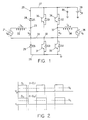
- Figure 1 is a schematic circuit diagram of a power conversion apparatus in accordance with the invention with input and output control.
- Figure 2 are illustrative voltage waveforms for DC modulation of the conversion apparatus of Figure 1.
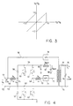
- Figure 3 is a plot showing the locus of possible values of the battery voltage for the conversion apparatus of Figure 1.
- Fig. 4 is a schematic circuit diagram for a UPS system utilizing the present invention.
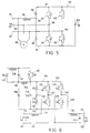
- Fig. 5 is a schematic circuit diagram of a single phase to three phase converter incorporating the conversion apparatus of the present invention.
- Fig. 6 is a schematic circuit diagram of a UPS power conversion apparatus utilizing a resonant DC link connected to the battery.
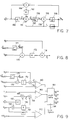
- Fig. 7 is a block diagram of a load side controller for a USP system in accordance with the invention.
- Fig. 8 is a block diagram of the synthesis of the input AC line reference I * s .
- Fig. 9 is a block diagram of a controller for the UPS system of Fig. 4 which accomplishes simultaneous control of the input and the output.
- Fig. 10 are waveforms for the resonant DC link inversion apparatus of Fig. 6 including output voltage, inductor current, inverter line to line voltage, and inductor current, supply voltage, and supply current.
- FIG. 1 A schematic circuit diagram of the basic power conversion apparatus of the invention is shown generally at 20 in Fig. 1.
- the apparatus receives AC power from a single phase source 21, which may be AC power mains, through an input inductor 22, which may represent an input transformer inductance.
- the inductor 22 is connected to a node 23 between a pair of diodes 24 and 25 to rectify the input AC current passed through the inductor 22 to a DC current and a DC voltage between DC bus lines 27 and 28.
- Also connected across the DC bus lines 27 and 28 is a inverter bridge formed of gate controlled active switching devices 30, 31, 34 and 35. Each of these switches, which may be bipolar junction transistors, typically would include antiparallel diodes as shown in Fig. 1.
- the electrical connection between the switches 30 and 31 is joined at a node 32 to a common neutral line 33 which extends from the input power source to the output load 36, represented as a voltage source in Fig. 1.
- the output of the bridge composed of the switches 30, 31, 34 and 35 is supplied from a connection at a node 37 to an output inductor 38 (which may represent an output transformer inductance) which delivers the current passed through it to the load 36.
- the backup storage battery 39, or output filter if required, is connected to the DC bus line 27, as is a smoothing capacitor 40.
- the inverter bridge operates under a pulse width modulation strategy which chooses one of three switching states (+1, 0 and -1).
- the choice of the zero state can be fullfilled by turning on switches 30 and 34 (zero positive, 0+) or 31 and 35 (zero negative, 0-) simultaneously, with no discernible difference from the point of view of the load. This fact represents an additional degree of freedom which can be exploited to control the AC line side current.
- the degree of control available on the input side depends strongly on the number of times the inverter is allowed to choose the zero state. This implies that a higher ratio of V B to V o is required to obtain good control on both sides.
- every selection of a non-zero state reduces the amount of control available for the input sides. Consequently, full control on both the input and output sides is only available over a restricted range of input and output voltages.
- V o D i . V B V s ⁇ D i .
- V B V o Consequently, if full control on input and output are to be obtained, V s must be greater than V o .
- V o -(1-D i ) .
- V B V s ⁇ D i .
- V B 1 + V o /V B
- the foregoing AC to DC to AC conversion apparatus can be adapted for UPS operation as shown in Fig. 4.
- the important requirements now include maintaining charge and discharge of the storage battery on the link, in addition to regulation of the input and output currents.
- the load side output may be controlled using a current regulator, in accordance with output voltage regulation and distortion requirements.
- the input side may also be current regulated, and the reference command is calculated based on battery charge and discharge needs as well as load demands.
- the UPS system in accordance with the present invention is shown generally at 50 in Fig. 4 and receives AC line power on AC terminals 51 and 52 from the power mains.
- One of the terminals 52 is connected to the common or neutral line 53 of the apparatus, while the other terminal 51 is connected to an input inductor 54 which supplies current to a node 55.
- the node 55 is connected between a pair of diodes 56 and 57 which are connected across the DC bus line 58 and ground.
- a bridge inverter formed of four active switching devices 59-62 is also connected across the DC bus 58 and ground in a manner similar to that described above with respect to the circuit of Fig. 1.
- the node 63 between the switching devices 59 and 60 is connected to the common line 53 and the node 64 between the switching devices 61 and 62 is the output voltage connection from the bridge. Also connected to the DC bus are a smoothing filter capacitor 65 to ground and a battery 66 through a filtering inductor 67.
- the output voltage from the bridge at the node 64 is supplied through an output inductor 70, a controllable static switch 71 and a line 72 to a tap in the primary of a transformer 74.
- the secondary of the transformer 74 is connected to an output line 75 leading to the load, with the capacitor 76 connected across the line 75 to filter output transients.
- a controllable static switch 78 is connected in a line from one of the AC input terminals 51 to the primary of the transformer 74.
- the system of Fig. 4 can operate as an on-line UPS and provide line conditioning and distubance rejection.
- the transformer tap is selected such that under low-line conditions the converter bridge formed of the devices 59-62 can adequately supply the load.
- the static switches 70 and 78 are activated to directly connect the load to the primary of the transformer.
- a particularly desirable feature of this circuit is the use of a common neutral connection between the input line at the terminal 52 and the output at the primary of the transformer 74.
- the AC to DC to AC conversion apparatus of the invention can also be adapted to be utilized as a single phase to three phase converter, as illustrated generally at 80 in Fig. 5.
- the system 80 receives single phase AC power at input terminals 81 and 82 but has a third terminal 83 on which is generated a voltage which effectively causes the power across the three terminals 81, 82 and 83 to be a three phase voltage which may be applied to a three phase load, such as the motor 84 illustrated in Fig. 5.
- the input voltage on one of the terminals 81 is provided through an input inductor 86 to a node 88 at which rectifying diodes 89 and 90 are joined.
- the output of the diodes 89 and 90 is provided to DC bus lines 91 and 92 across which is connected a bridge inverter composed of active switching devices 93-96. At a node 98 a connection is made between the switching devices 93 and 94 and the second AC input terminal 82. The output of the inverter at a node 99 connected between the switching devices 95 and 96 is connected to the third terminal 83.
- a capacitor 100 is connected across the DC bus to smooth out the voltage on the bus and provide a stored DC voltage across the bus lines.
- the output inverter composed of the switching elements 93-96 can supply voltage and current having an arbitrary phase/frequency relationship with the input, and because the neutral connection at which the input terminal 82 is connected to the node 98 is common, the inverter can be made to synthesize a waveform with the same voltage as the input, but phase shifted so as to generate a balanced, three phase voltage. This inverter can then be used to drive a three phase load indicated by the motor 84, for example, a constant speed induction machine.
- the conversion apparatus of the present invention can be readily adapted to be utilized as a soft switching resonant DC link inverter with frequencies which are an order of magnitude higher than conventional hard switching inverters.
- This resonant link circuit is illustrated generally at 110 in Fig. 6. Operation with bipolar junction transistors (BJT) darlingtons at 30 kHz for 15 kVA inverters is easily feasible. With IGBTs and new devices such as the MCT, link frequencies up to 60 kHz are possible. The circuit is easily realized at the multi-kilowatt power levels of interest.
- the use of a soft switching circuit achieves substantial benefits in terms of the size of filter components, acoustic noise, electromagnetic interference, and system efficiency.
- the high frequency DC link conversion apparatus 110 of Fig. 6 receives single phase power at input terminals 111 and 112, with one of the terminals connected to an input inductor 114 and the other connected to a common output line 115.
- the inductor 114 is connected to a node 116 that joins two diodes 118 and 119.
- the diodes 118 and 119 are connected between DC bus lines 120 and 121, as is an inverter composed of gate controlled active switching devices 123-126 connected in a bridge configuration.
- the junction between the switching devices 123 and 124 at a node 127 is connected to the common line 115, and the junction between the switching devices 125 and 126 at a node 128 is connected to an output line 129 leading to an output inductor 130 which extend to one of the output terminals 131, to which the UPS load may be connected.
- the other output terminal 132 is connected to the common line 115, and an output filtering capacitor 133 is connected between the terminals 131 and 132.
- a capacitor 135 is connected between the DC bus line 120 and 121 and charges to provide a DC voltage across these lines.
- the battery 137 is connected to the DC bus line 120 by a resonant link circuit composed of a series inductor 138 and an active switching device 140.
- a capacitor 141 and inductor 142 are also connected to the DC bus line 120 and are joined at a node 145 to which the battery is also connected.
- a capacitor 144 extends from the node 145 to connection to the other DC bus line 121.
- the switching of the device 140 can be controlled to provide a resonant DC link voltage on the DC bus 120 in a conventional manner. See, for example, D. M.
- FIG. 7 and 8 A variety of control options are available for providing simultaneous regulation of input and output currents as well as battery charging functions.
- a block schematic of a controller required for synthesizing to two reference currents I * s I * o is shown in Fig. 7 and 8. See, also, the article by Venkataramanan, et al., supra.
- a current regulator with reference and load feedforward is used to obtain good output regulation, especially in the presence of non-linear loads.
- the reference output voltage V * o is applied to a block 150 in Fig. 7 corresponding to the filter capacitor. This represents the fundamental component I * c that must flow in the capacitor if the desired output voltage is to be obtained.
- the current I * c is added at a junction 151 to the fundamental load current from I1 a line 152 to generate a current reference I * o for the converter section.
- the load current is considered to be a disturbance to the system, and is also compensated using feedforward on a line 154 to a summing junction 155 which also receives the value of I o through a current regulator 156. This approach gives extremely good dynamic characteristics as well as voltage regulation, even in the presence of substantial load non-linearities.
- the output of the junction 155 is integrated (156) to provide the output voltage V o which is compared in a summing junction 160 with the reference V * o and the difference is passed through a proportional-integral compensator 162, the output of which is supplied to the summing junction 151.
- the input current reference V * s is derived from the dual requirements of DC bus regulation and battery charge and discharge requirements.
- the battery voltage V B is compared at a summing junction 170 with a reference voltage V * b att derived at 171 from the reference battery current I * b att and the differences is provided to a proportional-integral controller 172, the output of which is provided to a multiplying junction 174 which also receives the supply voltage V s .
- the proportional-integral controller is used to accomplish power balance, taking into account the powerflow into the battery.
- the output of the proportional-integral regulator is multiplied with the input supply voltage V s to realize a template for the input current waveform I * s .
- the discrete pulse modulated current regulator can be implemented in various ways. Most appealing appears to be an optimal cost function regulator. See the article by Vekatarmanan, et al., supra. Discrete pulse modulators (DMP) systems which allow the selection of optimal inverter states to fulfill defined cost functions are relatively easy to implement.
- the cost function J is calculated for all the four states (1,0+,0-,-1), and the state which realizes the lowest value is selected. This approach has been implemented in the past, but is fairly complex.
- a simpler implementation which gives very good performance uses the output voltage information.
- V o When ever V o is sufficiently large, it can drive the output inductor current I * o with sufficient slope to allow current control. Under these conditions, the inverter output is switched between an active vector (i.e., +1) and zero. This permits control of the input side current.
- V o Whenever the voltage V o is close to zero, the inverter is swtiched from one active state to another to control the inverter current, but with one resonant link cycle spent on the zero state.
- This implementation requires comparators checking on the instantaneous errors in the load and line side inductor currents and a signal indicating the presence of adequate back EMF. A simple state sequencer is then sufficient to generate the control functions needed.
- FIG. 9 A block diagram of the controller implemented in accordance with the foregoing procedures is illustrated in Fig. 9.
- the I * s reference is generated in the same manner as illustrated in Fig. 8, and yields a value I * s which is compared with the measured current value I s in a differential amplifier 180, the output of which is provided as an input to a logic circuit 181 which provides the gating control outputs to the four active switches in the inverter.
- Another input to the logic circuit 181 is provided from a differential operational amplifier 183 which receives at its two inputs the load current I1 and the signal obtained from the output of a summing junction 184 which receives inputs from another summing junction 185 and from a gain control circuit 186 which provides a constant, K, to the signal applied thereto.
- the inputs to the junction 185 are the output current I o and the reference voltage V * o passed through the capacitor 187.
- the input to the gain function 186 is provided from a summing junction 190 which compares the reference voltage V * o with V o .
- V o is also applied through an absolute value function 191 to one of the inputs of a differential amplifier 192 which recieves at its other input a scaled source voltage kV s .
- the output of the amplifier 192 is also provided to the logic circuit 181.
- the circuit 181 also receives a link sychronization signal on a line 194 which provides timing information to properly time the gating signals to the gates of the active switching devices in the inverter bridge.
- a conversion apparatus utilizing the resonant DC link converter of Fig. 6 was implemented using BJT darlington transistor modules switched at a link frequency of 27 KHz.
- a controller as described above with respect to Fig. 9 was utilized which incorporates feetforward concepts as well as a discrete pulse modulation strategy.
- the waveforms of Fig. 10 illustrate the proper regulation of the input and output currents as well as control boost operation from the AC line to the DC link.
- the graphs in Fig. 10 show filter output voltage (200), output inductor current I o (201), inverter line to line voltage (202), input inductor current (203), supply voltage (204), and supply current (205).
- the line to line inverter output voltage waveform confirms the modulation strategy where plus and minus 1 transmissions are only permitted under low back EMF conditions, and even then only after a one cycle wait at a zero state.
- the resonant DC link converter implementation also realizes the benefit of low acoustic noise; low electromagnetic interference, excellent harmonic performance and dynamic performance, and high efficiency.
- the conversion apparatus in accordance with the present invention allows the achievement of several advantageous features. These include the requirement for only four switches, or five with a low voltage battery and resonant link operation, boost control from the AC line to the DC link, independent control of both input and output sides, a common neutral between the input and output, line conditioning in addition to a UPS function, sinusoidal input AC line currents irrespective of the load current, and the accomplishment of battery charge and discharge control with no additional devices.
Landscapes
- Engineering & Computer Science (AREA)
- Power Engineering (AREA)
- Business, Economics & Management (AREA)
- Emergency Management (AREA)
- Inverter Devices (AREA)
- Dc-Dc Converters (AREA)
- Ac-Ac Conversion (AREA)
- Rectifiers (AREA)
- Charge And Discharge Circuits For Batteries Or The Like (AREA)
Claims (14)
- Appareil de conversion d'énergie électrique comprenant :(a) des bornes d'entrée de courant alternatif adaptées pour être connectées à une source (21) d'énergie en courant alternatif monophasé et des bornes de sortie de courant alternatif adaptées pour être connectées à une charge (36);(b) une paire de lignes omnibus (27, 28) pour courant continu;(c) un pont redresseur (24, 25) comprenant une paire de diodes redresseuses connectées à une des bornes d'entrée de courant alternatif pour redresser le courant qui leur est fourni et montées entre les lignes omnibus (27, 28) pour courant continu;(d) un dispositif (39, 40) d'emmagasinage d'énergie en courant continu connecté fonctionnellement de manière à fournir de l'énergie en courant continu aux lignes omnibus pour courant continu ;(e) un inverseur constitué par des dispositifs de commutation actifs (30, 31, 34, 35) à électrode de commande, connectés suivant une configuration en pont à double alternance aux lignes omnibus (27, 28) pour courant continu et comportant deux noeuds de sortie (32, 37), les noeuds de sortie du pont étant connectés aux bornes de sortie de l'appareil de conversion d'énergie électrique;(f) une ligne commune (33) qui est commune à une des bornes d'entrée de l'appareil, à une des bornes de sortie de l'appareil et à un (32) des noeuds dde sortie du pont; et(g) un moyen de commande (Figure 9) pour commander la commutation des dispositifs de commutation (30, 31, 34, 35) à électrode de commande pour fournir une énergie de sortie en courant alternatif à une fréquence sélectionnée aux bornes de sortie de l'appareil de conversion d'énergie électrique.
- Appareil selon la revendication 1, comprenant une bobine de self-induction d'entrée (22) montée entre la borne d'entrée de l'appareil qui est connectée au pont redresseur (24, 25) et le pont redresseur et une autre bobine de self-induction (38) connectée à la borne de sortie qui n'est pas connectée à la ligne commune (33).
- Appareil selon la revendication 1 ou 2, dans lequel le moyen de commande (Figure 9) est adapté pour effectuer une commande utilisant la modulation de largeur d'impulsions de la commutation des dispositifs de commutation (30, 31, 34, 35).
- Appareil selon la revendication 1, 2 ou 3, dans lequel le dispositif d'emmagasinage d'énergie en courant continu comprend une batterie (39) et l'appareil est agencé de manière à fonctionner comme une source d'alimentation permanente pour fournir, à partir de la batterie (39), une énergie en courant alternatif aux bornes de sortie quand l'énergie électrique n'est pas fournie aux bornes d'entrée de l'appareil.
- Appareil selon la revendication 4, dans lequel le moyen de commande (Figure 9) assure en outre une circulation de courant redressé à partir des bornes d'entrée de courant alternatif pour charger la batterie (39) pendant les périodes de fonctionnement de l'appareil au cours desquelles le courant de la batterie n'est pas demandé.
- Appareil selon la revendication 4 ou 5, comprenant une ligne de dérivation s'étendant depuis une (51) des bornes d'entrée (51, 52) de l'appareil jusqu'à une des bornes de sortie de l'appareil et un dispositif de commutation commandé (78) monté dans la ligne de dérivation pour permettre à l'énergie en courant alternatif en provenance des bornes d'entrée (51, 52) d'être fournie directement aux bornes de sortie, dans des conditions normales de fonctionnement, quand le courant peut être obtenu à partir du système d'énergie en courant alternatif pour être fourni aux bornes d'entrée (51, 52).
- Appareil selon la revendication 6, comprenant, en outre, un dispositif de commutation (71) pouvant être commandé et monté dans une ligne menant à une borne de sortie depuis l'appareil pour être commuté de façon commandée de manière à isoler l'appareil vis-à-vis des bornes de sortie quand le courant est fourni à partir des lignes pour courant alternatif directement aux bornes de sortie.
- Appareil selon la revendication 6 ou 7, comprenant, en oure, un transformateur (74) connecté aux bornes de sortie de l'appareil, à l'endroit d'une prise (72) du primaire, et dans lequel la ligne de dérivation est connectée aux bornes d'extrémité du primaire du transformateur, le secondaire du transformateur comportant des bornes (75) qui peuvent être connectées à une charge.
- Appareil selon l'une quelconque des revendications précédentes, comprenant un moyen (138, 140), formant liaison accordée pour courant continu, monté entre le dispositif (137) d'emmagasinage d'énergie en courant continu et la ligne omnibus (120) pour courant continu, en vue d'assurer un transfert à résonnance d'énergie en courant continu à partir du dispositif (137) d'emmagasinage de courant continu vers la ligne omnibus (120) pour courant continu à une haute fréquence sélectionnée.
- Appareil selon la revendication 9, dans lequel le moyen formant liaison accordée comprend un dispositif de commutation (140) à électrode de commande, monté entre le dispositif (137) d'emmagasinage d'énergie en courant continu et la ligne omnibus (120) pour courant continu (120).
- Appareil selon l'une quelconque des revendications précédentes, dans lequel le moyen de commande (Figure 9) utilise une modulation d'impulsions discrètes pour commander les dispositifs de commutation (118, 119, 123, 124) à électrode de commande.
- Appareil selon l'une quelconque des revendications précédentes, dans lequel le moyen de commande (Figure 9) contrôle le courant de source de bornes d'entrée (Vbus), la tension (Es) de source de bornes d'entrée, le courant (Io) de bornes de sortie et la tension (Vo) de bornes de sortie, et utilise ces signaux pour commander les dispositifs de commutation à la manière d'une boucle fermée afin de commander le système pour chercher à suivre une tension de sortie, un courant de source d'entrée et un courant de charge de sortie désirés.
- Appareil selon la revendication 1, qui est adapté pour convertir une entrée de courant alternatif monophasé en une sortie de courant alternatif triphasé, dans lequel les bornes d'entrée (81, 82) sont connectées à une paire de lignes d'entrée, une première des lignes d'entrée comportant une bobine de self-induction d'entrée (86) qui y est connectée ; le dispositif (100) d'emmagasinage d'énergie en courant continu est connecté aux lignes omnibus (91, 92); le pont redresseur comprend une paire de diodes redresseuses (89, 90) connectées entre les lignes omnibus pour courant continu, le noeud (88) reliant les diodes (89, 90) étant connecté à la première ligne d'entrée pour recevoir le courant traversant la bobine de self induction (86) d'entrée; le noeud (98) d'inverseur entre deux des dispositifs de commutation (93, 94) est connecté à la seconde ligne d'entrée de courant alternatif dans laquelle n'est pas montée la bobine de self-induction d'entrée et qui constitue ladite ligne commune; une troisième ligne (83) est connectée au noeud (99) entre l'autre (95, 96) des dispositifs de commutation à électrode de commande du pont pour fournir la tension de sortie entre ces deux dispositifs de commutation (95, 96), les deux bornes (81, 82) d'entrée de courant alternatif et la troisième ligne (83) constituant les bornes de sortie triphasées du dispositif; et le moyen de commande commande la commutation des dispositifs de commutation du pont inverseur pour fournir aux trois bornes de l'appareil une tension alternative qui constitue trois tensions de phase.
- Appareil selon l'une quelconque des revendications précédentes, dans lequel l'inverseur comprend quatre desdits dispositifs de commutation (93, 94, 95, 96).
Applications Claiming Priority (2)
| Application Number | Priority Date | Filing Date | Title |
|---|---|---|---|
| US07/414,896 US5017800A (en) | 1989-09-29 | 1989-09-29 | AC to DC to AC power conversion apparatus with few active switches and input and output control |
| US414896 | 1999-10-08 |
Publications (3)
| Publication Number | Publication Date |
|---|---|
| EP0420628A2 EP0420628A2 (fr) | 1991-04-03 |
| EP0420628A3 EP0420628A3 (en) | 1991-08-28 |
| EP0420628B1 true EP0420628B1 (fr) | 1994-11-30 |
Family
ID=23643463
Family Applications (1)
| Application Number | Title | Priority Date | Filing Date |
|---|---|---|---|
| EP19900310561 Expired - Lifetime EP0420628B1 (fr) | 1989-09-29 | 1990-09-27 | Dispositif de conversion de puissance AC-DC-AC avec peu de commutateurs actifs et régulation d'entrée et de sortie |
Country Status (8)
| Country | Link |
|---|---|
| US (1) | US5017800A (fr) |
| EP (1) | EP0420628B1 (fr) |
| JP (1) | JPH03195375A (fr) |
| KR (1) | KR910007224A (fr) |
| AT (1) | ATE114892T1 (fr) |
| CA (1) | CA2025847A1 (fr) |
| DE (1) | DE69014530T2 (fr) |
| ES (1) | ES2064658T3 (fr) |
Families Citing this family (126)
| Publication number | Priority date | Publication date | Assignee | Title |
|---|---|---|---|---|
| WO1999027640A2 (fr) * | 1997-11-21 | 1999-06-03 | Continental Teves Ag & Co. Ohg | Procede et circuit pour la production d'un signal de reglage a modulation d'impulsions en largeur pour un actionneur a courant continu |
| US4797907A (en) * | 1987-08-07 | 1989-01-10 | Diasonics Inc. | Battery enhanced power generation for mobile X-ray machine |
| JPH03230764A (ja) * | 1990-02-01 | 1991-10-14 | Toshiba Corp | Pwm制御による電源装置 |
| US5099410A (en) * | 1990-11-13 | 1992-03-24 | Wisconsin Alumni Research Foundation | Single phase ac power conversion apparatus |
| DE4142534A1 (de) * | 1990-12-28 | 1992-07-09 | Sawafuji Electric Co Ltd | Rotationskompressor-steuersystem fuer ein elektrisches kuehlgeraet |
| US5101145A (en) * | 1991-02-01 | 1992-03-31 | Allen-Bradley Company, Inc. | Velocity proportional integral regulator with negative feedforward to control response of torque disturbances |
| US5172009A (en) * | 1991-02-25 | 1992-12-15 | Regents Of The University Of Minnesota | Standby power supply with load-current harmonics neutralizer |
| US5315497A (en) * | 1991-11-07 | 1994-05-24 | Premier Power, Inc. | Symmetrical universal AC-AC power conditioner |
| US5241217A (en) * | 1991-11-07 | 1993-08-31 | Premier Power, Inc. | UPS with input commutation between AC and DC sources of power |
| JPH0548590U (ja) * | 1991-11-22 | 1993-06-25 | 日本オーチス・エレベータ株式会社 | コンバータの電流制御回路 |
| US5324990A (en) * | 1992-04-03 | 1994-06-28 | Cunningham John C | Voltage inverter power conservation circuit |
| US5272616A (en) * | 1992-04-21 | 1993-12-21 | Wisconsin Alumni Research Foundation | Single phase to three phase power converter for motor loads |
| US5307004A (en) * | 1992-07-06 | 1994-04-26 | Carsten Bruce W | Soft switching boost and buck regulators |
| DE4237843A1 (de) * | 1992-11-10 | 1994-05-11 | Philips Patentverwaltung | Schaltungsanordnung zum Betreiben einer induktiven Last |
| US5341075A (en) * | 1993-03-10 | 1994-08-23 | A.C. Propulsion, Inc. | Combined motor drive and battery recharge system |
| JP2918430B2 (ja) * | 1993-04-02 | 1999-07-12 | 三菱電機株式会社 | 電力変換装置 |
| ES2076860B1 (es) * | 1993-05-03 | 1996-05-01 | Iberdrola Sa | Acondicionador de linea para reduccion o eliminacion de perturbaciones. |
| US5402053A (en) * | 1993-08-26 | 1995-03-28 | Wisconsin Alumni Research Foundation | Single phase to three phase converter capable of variable speed motor operation |
| US5612599A (en) * | 1994-04-25 | 1997-03-18 | Ricoh Company, Ltd. | DC brushless motor driving device, DC brushless motor, and image forming device using the driving device and brushless motor |
| US5570279A (en) * | 1994-09-21 | 1996-10-29 | The Research And Development Institute, Inc. At Montana State University | PWM converters for three phase AC power control and AC to DC conversion |
| WO1996009686A1 (fr) * | 1994-09-21 | 1996-03-28 | The Research And Development Institute At Montana State University | Convertisseurs a modulation d'impulsions en largeur pour regulation de courant alternatif triphase et conversion de courant alternatif en courant continu, et dispositifs d'utilisation speciaux |
| US5602725A (en) * | 1994-09-21 | 1997-02-11 | The Research And Development Institute At Montana State University | Special purpose power control devices using 3-phase PWM converters for three phase AC power |
| AU3572995A (en) * | 1994-09-30 | 1996-04-26 | Grinaker Electronics Limited | Ac to dc converter |
| US5610805A (en) * | 1995-01-10 | 1997-03-11 | Cambridge Continuous Power | Uninterruptible power supply with a back-up battery coupled across the a.c. input |
| US5834858A (en) * | 1995-04-05 | 1998-11-10 | Electronic Design & Manufacturing Inc. | Emergency power supply |
| US5568370A (en) * | 1995-06-09 | 1996-10-22 | Vse Corporation | Tactical power adapter |
| US5661390A (en) * | 1995-06-23 | 1997-08-26 | Electric Power Research Institute, Inc. | Inverter-fed motor drive with EMI suppression |
| JPH0934564A (ja) * | 1995-07-18 | 1997-02-07 | Chiyoda:Kk | 入力波形追従型交流電源装置 |
| US6111392A (en) * | 1996-09-09 | 2000-08-29 | Matsushita Electric Works, Ltd. | Power source device including a plurality of switching circuit for power conversion with switching elements used in common |
| US7269034B2 (en) | 1997-01-24 | 2007-09-11 | Synqor, Inc. | High efficiency power converter |
| JP2002514378A (ja) | 1997-01-24 | 2002-05-14 | シンクォール・インコーポレーテッド | 高効率電力変換装置 |
| ID23796A (id) * | 1997-01-31 | 2000-05-11 | Silver Power Conversion Llc | Pemasok daya yang tak dapat terputus |
| DE19851831B4 (de) * | 1997-11-10 | 2016-04-07 | Fuji Electric Co., Ltd. | Mehrphasen-Stromrichter |
| US8497330B2 (en) * | 1997-12-08 | 2013-07-30 | Univation Technologies, Llc | Methods for polymerization using spray dried and slurried catalyst |
| US6242545B1 (en) * | 1997-12-08 | 2001-06-05 | Univation Technologies | Polymerization catalyst systems comprising substituted hafinocenes |
| US5969957A (en) * | 1998-02-04 | 1999-10-19 | Soft Switching Technologies Corporation | Single phase to three phase converter |
| US5994793A (en) * | 1998-05-11 | 1999-11-30 | Multipower, Inc. | Uninterruptible power supply with plurality of inverters |
| US6154057A (en) * | 1998-12-07 | 2000-11-28 | Motorola, Inc. | Bi-directional voltage translator |
| US6404658B1 (en) | 1999-05-13 | 2002-06-11 | American Power Conversion | Method and apparatus for converting a DC voltage to an AC voltage |
| US6804129B2 (en) * | 1999-07-22 | 2004-10-12 | 02 Micro International Limited | High-efficiency adaptive DC/AC converter |
| US6259615B1 (en) | 1999-07-22 | 2001-07-10 | O2 Micro International Limited | High-efficiency adaptive DC/AC converter |
| US6483730B2 (en) | 1999-08-13 | 2002-11-19 | Powerware Corporation | Power converters with AC and DC operating modes and methods of operation thereof |
| US6160722A (en) * | 1999-08-13 | 2000-12-12 | Powerware Corporation | Uninterruptible power supplies with dual-sourcing capability and methods of operation thereof |
| US6819576B2 (en) | 1999-08-13 | 2004-11-16 | Powerware Corporation | Power conversion apparatus and methods using balancer circuits |
| US6266260B1 (en) | 1999-09-03 | 2001-07-24 | Powerware Corporation | Inverter having center switch and uninterruptible power supply implementing same |
| WO2001065659A2 (fr) * | 2000-02-29 | 2001-09-07 | Powerware Corporation | Convertisseurs de puissance fonctionnant en ca et cc et procedes d'exploitation associes |
| US6531831B2 (en) | 2000-05-12 | 2003-03-11 | O2Micro International Limited | Integrated circuit for lamp heating and dimming control |
| US6501234B2 (en) * | 2001-01-09 | 2002-12-31 | 02 Micro International Limited | Sequential burst mode activation circuit |
| US6570344B2 (en) | 2001-05-07 | 2003-05-27 | O2Micro International Limited | Lamp grounding and leakage current detection system |
| US6741061B2 (en) * | 2001-05-24 | 2004-05-25 | Comair Rotron, Inc. | Efficient stator |
| US6631080B2 (en) | 2001-06-06 | 2003-10-07 | Hybrid Power Generation Systems Llc | Systems and methods for boosting DC link voltage in turbine generators |
| US7515446B2 (en) * | 2002-04-24 | 2009-04-07 | O2Micro International Limited | High-efficiency adaptive DC/AC converter |
| US6856519B2 (en) | 2002-05-06 | 2005-02-15 | O2Micro International Limited | Inverter controller |
| TWI291282B (en) * | 2002-06-03 | 2007-12-11 | Fuji Electric Co Ltd | Power converter |
| US6873322B2 (en) * | 2002-06-07 | 2005-03-29 | 02Micro International Limited | Adaptive LCD power supply circuit |
| US6756769B2 (en) | 2002-06-20 | 2004-06-29 | O2Micro International Limited | Enabling circuit for avoiding negative voltage transients |
| US6949912B2 (en) | 2002-06-20 | 2005-09-27 | 02Micro International Limited | Enabling circuit for avoiding negative voltage transients |
| US6778415B2 (en) * | 2003-01-22 | 2004-08-17 | O2Micro, Inc. | Controller electrical power circuit supplying energy to a display device |
| US6984897B2 (en) * | 2003-01-23 | 2006-01-10 | Spellman High Voltage Electronics Corporation | Electro-mechanical energy conversion system having a permanent magnet machine with stator, resonant transfer link and energy converter controls |
| US7057611B2 (en) * | 2003-03-25 | 2006-06-06 | 02Micro International Limited | Integrated power supply for an LCD panel |
| US6936975B2 (en) * | 2003-04-15 | 2005-08-30 | 02Micro International Limited | Power supply for an LCD panel |
| US6897698B1 (en) | 2003-05-30 | 2005-05-24 | O2Micro International Limited | Phase shifting and PWM driving circuits and methods |
| JP4325284B2 (ja) * | 2003-06-04 | 2009-09-02 | トヨタ自動車株式会社 | 電圧変換装置 |
| US7102251B2 (en) | 2003-08-22 | 2006-09-05 | Distributed Power, Inc. | Bi-directional multi-port inverter with high frequency link transformer |
| US7612472B2 (en) * | 2004-01-23 | 2009-11-03 | American Power Conversion Corporation | Method and apparatus for monitoring energy storage devices |
| US7446433B2 (en) * | 2004-01-23 | 2008-11-04 | American Power Conversion Corporation | Methods and apparatus for providing uninterruptible power |
| US7379305B2 (en) * | 2004-01-23 | 2008-05-27 | American Power Conversion Corporation | Modular UPS |
| US7046534B2 (en) * | 2004-02-09 | 2006-05-16 | Fraunhofer-Gesellschaft zur Förderung der angewandten Forschung e. V. | DC/AC converter to convert direct electric voltage into alternating voltage or into alternating current |
| US7394209B2 (en) * | 2004-02-11 | 2008-07-01 | 02 Micro International Limited | Liquid crystal display system with lamp feedback |
| US7327587B2 (en) * | 2004-09-30 | 2008-02-05 | General Electric Company | System and method for power conversion |
| US7402921B2 (en) * | 2005-04-21 | 2008-07-22 | American Power Conversion Corporation | Method and apparatus for providing uninterruptible power |
| WO2007018537A1 (fr) * | 2005-08-05 | 2007-02-15 | Tm Ge Automation Systems, Llc | Systeme et procede de demarrage d'un moteur a rotor bobine |
| KR100616237B1 (ko) * | 2005-05-21 | 2006-08-28 | 명지대학교 산학협력단 | 펄스 다중화 보조회로를 이용한 다중펄스 전압원 컨버터 |
| US7336114B2 (en) * | 2006-04-05 | 2008-02-26 | Wionics Research | High-speed latching technique and application to frequency dividers |
| US7499524B2 (en) * | 2006-04-27 | 2009-03-03 | General Electric Company | Methods and apparatus for mobile imaging systems |
| US8327656B2 (en) * | 2006-08-15 | 2012-12-11 | American Power Conversion Corporation | Method and apparatus for cooling |
| US8322155B2 (en) * | 2006-08-15 | 2012-12-04 | American Power Conversion Corporation | Method and apparatus for cooling |
| US9568206B2 (en) * | 2006-08-15 | 2017-02-14 | Schneider Electric It Corporation | Method and apparatus for cooling |
| US7705489B2 (en) * | 2006-09-08 | 2010-04-27 | American Power Conversion Corporation | Method and apparatus for providing uninterruptible power |
| US7522705B2 (en) * | 2006-11-14 | 2009-04-21 | General Electric Company | Power handling methods and apparatus |
| US7681404B2 (en) * | 2006-12-18 | 2010-03-23 | American Power Conversion Corporation | Modular ice storage for uninterruptible chilled water |
| US20080142068A1 (en) * | 2006-12-18 | 2008-06-19 | American Power Conversion Corporation | Direct Thermoelectric chiller assembly |
| US8425287B2 (en) * | 2007-01-23 | 2013-04-23 | Schneider Electric It Corporation | In-row air containment and cooling system and method |
| US7688048B2 (en) * | 2007-02-21 | 2010-03-30 | American Power Conversion Corporation | 3-phase high power UPS |
| CN101755495B (zh) | 2007-05-15 | 2013-10-16 | 美国能量变换公司 | 用来管理设施供电和冷却的方法和系统 |
| US8116105B2 (en) | 2008-02-07 | 2012-02-14 | American Power Conversion Corporation | Systems and methods for uninterruptible power supply control |
| US9519517B2 (en) * | 2009-02-13 | 2016-12-13 | Schneider Electtic It Corporation | Data center control |
| US8385091B2 (en) | 2009-08-20 | 2013-02-26 | Electric IT Corporation | 3-phase high-power UPS |
| US8575779B2 (en) | 2010-02-18 | 2013-11-05 | Alpha Technologies Inc. | Ferroresonant transformer for use in uninterruptible power supplies |
| US8552589B2 (en) | 2010-05-14 | 2013-10-08 | Schneider Electric It Corporation | Digital control method for operating the UPS systems in parallel |
| US8698354B2 (en) | 2010-11-05 | 2014-04-15 | Schneider Electric It Corporation | System and method for bidirectional DC-AC power conversion |
| US8335096B2 (en) | 2010-11-12 | 2012-12-18 | Don Roy Sauer | Rectifier less bidirectional AC to DC converter |
| CN102116850B (zh) * | 2010-12-09 | 2013-02-13 | 中国北车集团大连机车车辆有限公司 | 整流器试验装置及方法 |
| US8878389B2 (en) | 2011-01-11 | 2014-11-04 | Schneider Electric It Corporation | Method and apparatus for providing uninterruptible power |
| US8803361B2 (en) | 2011-01-19 | 2014-08-12 | Schneider Electric It Corporation | Apparatus and method for providing uninterruptible power |
| BR112013018804A2 (pt) | 2011-01-23 | 2020-09-01 | Alpha Technologies Inc. | fontes de alimentação ininterruptíveis para uso em uma rede distribuída |
| WO2012148512A1 (fr) | 2011-01-23 | 2012-11-01 | Alpha Technologies Inc. | Systèmes et procédé de commutation pour alimentation électrique non interruptible |
| US8884464B2 (en) | 2011-08-29 | 2014-11-11 | Schneider Electric It Corporation | Twin boost converter with integrated charger for UPS system |
| CN102355125B (zh) * | 2011-09-09 | 2014-04-23 | 北京索英电气技术有限公司 | 变流器的软启动电路 |
| CN103959634B (zh) * | 2011-11-17 | 2017-09-01 | 通用电气技术有限公司 | 用于hvdc应用的混合ac/dc转换器 |
| CN104137105B (zh) | 2011-12-22 | 2017-07-11 | 施耐德电气It公司 | 关于瞬时事件对数据中心中的温度的影响分析 |
| US9830410B2 (en) | 2011-12-22 | 2017-11-28 | Schneider Electric It Corporation | System and method for prediction of temperature values in an electronics system |
| US9234916B2 (en) | 2012-05-11 | 2016-01-12 | Alpha Technologies Inc. | Status monitoring cables for generators |
| CN103354383B (zh) * | 2013-04-28 | 2015-07-22 | 湖北汽车工业学院 | 超级电容充电装置 |
| US10199950B1 (en) | 2013-07-02 | 2019-02-05 | Vlt, Inc. | Power distribution architecture with series-connected bus converter |
| US10277067B2 (en) | 2013-10-30 | 2019-04-30 | Schneider Electric It Corporation | Power supply control |
| CN103580502A (zh) * | 2013-11-15 | 2014-02-12 | 华为技术有限公司 | 电源转换电路及控制直流-交流电路的方法 |
| KR102120955B1 (ko) * | 2013-11-22 | 2020-06-10 | 삼성전자주식회사 | 시간 지연 기법을 이용하여 역전류 누설을 제거하는 역전류 보상 회로 및 능동형 정류기 |
| CN103715754A (zh) * | 2013-12-17 | 2014-04-09 | 华为技术有限公司 | 一种ups和供电系统 |
| WO2015167568A1 (fr) * | 2014-05-01 | 2015-11-05 | Schneider Electric It Corporation | Commande d'alimentation électrique |
| JP6372182B2 (ja) * | 2014-06-17 | 2018-08-15 | 富士通株式会社 | 信号変換回路および電源装置 |
| EP3161925B1 (fr) * | 2014-06-27 | 2021-08-04 | Schneider Electric IT Corporation | Topologie d'énergie à 3 niveaux |
| US10029573B2 (en) | 2014-08-27 | 2018-07-24 | Ford Global Technologies, Llc | Vehicle battery charging system notification |
| US9484844B1 (en) | 2015-04-16 | 2016-11-01 | Glen Floreancig | Circuit and method for reducing inrush current of phase converter motor |
| CA2997565A1 (fr) | 2015-09-11 | 2017-03-16 | Invertedpower Pty Ltd | Controleur pour charge inductive ayant un ou plusieurs enroulements inductifs |
| WO2018204964A1 (fr) | 2017-05-08 | 2018-11-15 | Invertedpowder Pty Ltd | Station de charge de véhicule |
| US11479139B2 (en) | 2015-09-11 | 2022-10-25 | Invertedpower Pty Ltd | Methods and systems for an integrated charging system for an electric vehicle |
| EP3347979A4 (fr) | 2015-09-13 | 2019-01-16 | Alpha Technologies Inc. | Systèmes et procédés de commande d'alimentation |
| US10381867B1 (en) | 2015-10-16 | 2019-08-13 | Alpha Technologeis Services, Inc. | Ferroresonant transformer systems and methods with selectable input and output voltages for use in uninterruptible power supplies |
| US10566831B2 (en) * | 2017-03-05 | 2020-02-18 | Oather A McClung, Jr. | Zero energy loss efficient power supply responsive to connection state and utilization device control |
| EP3652604A4 (fr) | 2017-07-14 | 2021-03-17 | Alpha Technologies Services, Inc. | Systèmes et procédés d'alimentation en courant alternatif à régulation de tension |
| EP3847741A4 (fr) * | 2018-09-06 | 2022-05-25 | Cornell University | Convertisseur de puissance à haute densité de puissance et circuit d'alimentation sans coupure et procédés |
| JP7088860B2 (ja) * | 2019-02-12 | 2022-06-21 | ニチコン株式会社 | 交流電力変換装置 |
| US11431191B2 (en) * | 2019-07-24 | 2022-08-30 | Constellation Energy Generation, Llc | Methods and systems for providing power |
| CN114069819A (zh) * | 2020-08-07 | 2022-02-18 | 台达电子工业股份有限公司 | 具有三阶层切换电路的转换装置及三阶层切换电路的操作方法 |
| KR20250086699A (ko) * | 2023-10-10 | 2025-06-13 | 가부시키가이샤 티마이크 | 무정전 전원 장치 |
Citations (1)
| Publication number | Priority date | Publication date | Assignee | Title |
|---|---|---|---|---|
| DE3702834A1 (de) * | 1987-01-30 | 1988-08-11 | Reo Boris Von Wolff | Wechselspannungsstabilisator |
Family Cites Families (5)
| Publication number | Priority date | Publication date | Assignee | Title |
|---|---|---|---|---|
| GB2111326B (en) * | 1981-12-01 | 1985-07-24 | Chloride Group Ltd | No-break power supply |
| JPS611269A (ja) * | 1984-06-08 | 1986-01-07 | Tokai T R W Kk | インバ−タ装置と負荷結線方法 |
| JPS611270A (ja) * | 1984-06-08 | 1986-01-07 | Tokai T R W Kk | インバ−タ装置と負荷結線方法 |
| JP2911447B2 (ja) * | 1986-04-01 | 1999-06-23 | 三菱電機株式会社 | 電動機の制御装置 |
| JP2677409B2 (ja) * | 1988-09-19 | 1997-11-17 | 勲 高橋 | インバータ装置 |
-
1989
- 1989-09-29 US US07/414,896 patent/US5017800A/en not_active Expired - Fee Related
-
1990
- 1990-09-20 CA CA 2025847 patent/CA2025847A1/fr not_active Abandoned
- 1990-09-27 EP EP19900310561 patent/EP0420628B1/fr not_active Expired - Lifetime
- 1990-09-27 AT AT90310561T patent/ATE114892T1/de active
- 1990-09-27 DE DE69014530T patent/DE69014530T2/de not_active Expired - Fee Related
- 1990-09-27 ES ES90310561T patent/ES2064658T3/es not_active Expired - Lifetime
- 1990-09-28 JP JP2260306A patent/JPH03195375A/ja active Pending
- 1990-09-28 KR KR1019900015559A patent/KR910007224A/ko not_active Withdrawn
Patent Citations (1)
| Publication number | Priority date | Publication date | Assignee | Title |
|---|---|---|---|---|
| DE3702834A1 (de) * | 1987-01-30 | 1988-08-11 | Reo Boris Von Wolff | Wechselspannungsstabilisator |
Also Published As
| Publication number | Publication date |
|---|---|
| EP0420628A2 (fr) | 1991-04-03 |
| DE69014530D1 (de) | 1995-01-12 |
| KR910007224A (ko) | 1991-04-30 |
| DE69014530T2 (de) | 1995-04-06 |
| EP0420628A3 (en) | 1991-08-28 |
| US5017800A (en) | 1991-05-21 |
| ATE114892T1 (de) | 1994-12-15 |
| ES2064658T3 (es) | 1995-02-01 |
| JPH03195375A (ja) | 1991-08-26 |
| CA2025847A1 (fr) | 1991-03-30 |
Similar Documents
| Publication | Publication Date | Title |
|---|---|---|
| US5017800A (en) | AC to DC to AC power conversion apparatus with few active switches and input and output control | |
| US5172009A (en) | Standby power supply with load-current harmonics neutralizer | |
| Kwon et al. | Improved single-phase line-interactive UPS | |
| Venkataramanan et al. | Discrete pulse modulation strategies for high-frequency inverter systems | |
| Shimizu et al. | A unity power factor PWM rectifier with DC ripple compensation | |
| US6295215B1 (en) | AC power supply apparatus with economy mode and methods of operation thereof | |
| EP0500789B1 (fr) | Systeme d'alimentation ininterrompue a circuit ameliore de correction du facteur de puissance | |
| US6314007B2 (en) | Multi-mode power converters incorporating balancer circuits and methods of operation thereof | |
| Aburto et al. | An active power filter implemented with a three-level NPC voltage-source inverter | |
| US6762947B2 (en) | Control method and apparatus to reduce current through DC capacitor linking two static converters | |
| JP2000324852A (ja) | 太陽光発電用電流形インバータ装置 | |
| US12294295B2 (en) | Systems and methods of unwanted harmonic content removal for power conversion | |
| Anand et al. | ANPC switched-capacitor 19L inverter using SHE PWM for 1-ϕ HFAC PDS applications | |
| Lin et al. | Single-phase power-factor-correction AC/DC converters with three PWM control schemes | |
| US11777414B2 (en) | Interleaved power conversion systems and methods | |
| JPH11235040A (ja) | 3相高力率コンバータを有する電源装置 | |
| US6175510B1 (en) | Direct conversion uninterruptible power supply | |
| JP2527911B2 (ja) | Pwmコンバ―タ | |
| JPH11178216A (ja) | 無停電電源装置 | |
| JP3082849B2 (ja) | 無停電電源装置 | |
| Baronian et al. | An adaptive digital control of current source inverter suitable for parallel processing inverter systems | |
| JP2956372B2 (ja) | 無停電電源装置 | |
| Meena et al. | A Review of Design, Development, Control and Applications of DC− DC Converters | |
| CN120855637B (zh) | 一种ups前级模组及其控制方法 | |
| Cakanel et al. | Frequency control of DC/AC inverter |
Legal Events
| Date | Code | Title | Description |
|---|---|---|---|
| PUAI | Public reference made under article 153(3) epc to a published international application that has entered the european phase |
Free format text: ORIGINAL CODE: 0009012 |
|
| AK | Designated contracting states |
Kind code of ref document: A2 Designated state(s): AT BE CH DE DK ES FR GB GR IT LI LU NL SE |
|
| PUAL | Search report despatched |
Free format text: ORIGINAL CODE: 0009013 |
|
| AK | Designated contracting states |
Kind code of ref document: A3 Designated state(s): AT BE CH DE DK ES FR GB GR IT LI LU NL SE |
|
| 17P | Request for examination filed |
Effective date: 19911104 |
|
| 17Q | First examination report despatched |
Effective date: 19930524 |
|
| GRAA | (expected) grant |
Free format text: ORIGINAL CODE: 0009210 |
|
| AK | Designated contracting states |
Kind code of ref document: B1 Designated state(s): AT BE CH DE DK ES FR GB GR IT LI LU NL SE |
|
| PG25 | Lapsed in a contracting state [announced via postgrant information from national office to epo] |
Ref country code: GR Free format text: LAPSE BECAUSE OF FAILURE TO SUBMIT A TRANSLATION OF THE DESCRIPTION OR TO PAY THE FEE WITHIN THE PRESCRIBED TIME-LIMIT Effective date: 19941130 Ref country code: DK Effective date: 19941130 Ref country code: AT Effective date: 19941130 |
|
| REF | Corresponds to: |
Ref document number: 114892 Country of ref document: AT Date of ref document: 19941215 Kind code of ref document: T |
|
| ITF | It: translation for a ep patent filed | ||
| REF | Corresponds to: |
Ref document number: 69014530 Country of ref document: DE Date of ref document: 19950112 |
|
| REG | Reference to a national code |
Ref country code: ES Ref legal event code: FG2A Ref document number: 2064658 Country of ref document: ES Kind code of ref document: T3 |
|
| PG25 | Lapsed in a contracting state [announced via postgrant information from national office to epo] |
Ref country code: SE Effective date: 19950228 |
|
| EN | Fr: translation not filed | ||
| PG25 | Lapsed in a contracting state [announced via postgrant information from national office to epo] |
Ref country code: LU Free format text: LAPSE BECAUSE OF NON-PAYMENT OF DUE FEES Effective date: 19950930 Ref country code: LI Effective date: 19950930 Ref country code: CH Effective date: 19950930 Ref country code: BE Effective date: 19950930 |
|
| PLBE | No opposition filed within time limit |
Free format text: ORIGINAL CODE: 0009261 |
|
| STAA | Information on the status of an ep patent application or granted ep patent |
Free format text: STATUS: NO OPPOSITION FILED WITHIN TIME LIMIT |
|
| EN | Fr: translation not filed |
Free format text: BO 95/17 DU 950428: "LA MENTION DU DEFAUT DE LA REMISE DE LA TRADUCTION EST A CONSIDERER COMME NULLE ET NON AVENUE" |
|
| 26N | No opposition filed | ||
| ET | Fr: translation filed | ||
| BERE | Be: lapsed |
Owner name: WISCONSIN ALUMNI RESEARCH FOUNDATION Effective date: 19950930 |
|
| PG25 | Lapsed in a contracting state [announced via postgrant information from national office to epo] |
Ref country code: NL Effective date: 19960401 |
|
| REG | Reference to a national code |
Ref country code: CH Ref legal event code: PL |
|
| NLV4 | Nl: lapsed or anulled due to non-payment of the annual fee |
Effective date: 19960401 |
|
| PGFP | Annual fee paid to national office [announced via postgrant information from national office to epo] |
Ref country code: FR Payment date: 20010911 Year of fee payment: 12 |
|
| PGFP | Annual fee paid to national office [announced via postgrant information from national office to epo] |
Ref country code: ES Payment date: 20010920 Year of fee payment: 12 |
|
| PGFP | Annual fee paid to national office [announced via postgrant information from national office to epo] |
Ref country code: GB Payment date: 20010926 Year of fee payment: 12 |
|
| PGFP | Annual fee paid to national office [announced via postgrant information from national office to epo] |
Ref country code: DE Payment date: 20011015 Year of fee payment: 12 |
|
| REG | Reference to a national code |
Ref country code: GB Ref legal event code: IF02 |
|
| PG25 | Lapsed in a contracting state [announced via postgrant information from national office to epo] |
Ref country code: GB Free format text: LAPSE BECAUSE OF NON-PAYMENT OF DUE FEES Effective date: 20020927 |
|
| PG25 | Lapsed in a contracting state [announced via postgrant information from national office to epo] |
Ref country code: ES Free format text: LAPSE BECAUSE OF NON-PAYMENT OF DUE FEES Effective date: 20020928 |
|
| PG25 | Lapsed in a contracting state [announced via postgrant information from national office to epo] |
Ref country code: DE Free format text: LAPSE BECAUSE OF NON-PAYMENT OF DUE FEES Effective date: 20030401 |
|
| GBPC | Gb: european patent ceased through non-payment of renewal fee |
Effective date: 20020927 |
|
| PG25 | Lapsed in a contracting state [announced via postgrant information from national office to epo] |
Ref country code: FR Free format text: LAPSE BECAUSE OF NON-PAYMENT OF DUE FEES Effective date: 20030603 |
|
| REG | Reference to a national code |
Ref country code: FR Ref legal event code: ST |
|
| REG | Reference to a national code |
Ref country code: ES Ref legal event code: FD2A Effective date: 20031011 |
|
| PG25 | Lapsed in a contracting state [announced via postgrant information from national office to epo] |
Ref country code: IT Free format text: LAPSE BECAUSE OF NON-PAYMENT OF DUE FEES;WARNING: LAPSES OF ITALIAN PATENTS WITH EFFECTIVE DATE BEFORE 2007 MAY HAVE OCCURRED AT ANY TIME BEFORE 2007. THE CORRECT EFFECTIVE DATE MAY BE DIFFERENT FROM THE ONE RECORDED. Effective date: 20050927 |