EP0420672A1 - Structure pour substrat semi-conducteur utilisée dans un dispositif IC à haute puissance - Google Patents
Structure pour substrat semi-conducteur utilisée dans un dispositif IC à haute puissance Download PDFInfo
- Publication number
- EP0420672A1 EP0420672A1 EP90310645A EP90310645A EP0420672A1 EP 0420672 A1 EP0420672 A1 EP 0420672A1 EP 90310645 A EP90310645 A EP 90310645A EP 90310645 A EP90310645 A EP 90310645A EP 0420672 A1 EP0420672 A1 EP 0420672A1
- Authority
- EP
- European Patent Office
- Prior art keywords
- layer
- region
- type
- junction
- elements
- Prior art date
- Legal status (The legal status is an assumption and is not a legal conclusion. Google has not performed a legal analysis and makes no representation as to the accuracy of the status listed.)
- Granted
Links
Images






Classifications
-
- H—ELECTRICITY
- H10—SEMICONDUCTOR DEVICES; ELECTRIC SOLID-STATE DEVICES NOT OTHERWISE PROVIDED FOR
- H10W—GENERIC PACKAGES, INTERCONNECTIONS, CONNECTORS OR OTHER CONSTRUCTIONAL DETAILS OF DEVICES COVERED BY CLASS H10
- H10W10/00—Isolation regions in semiconductor bodies between components of integrated devices
- H10W10/01—Manufacture or treatment
- H10W10/031—Manufacture or treatment of isolation regions comprising PN junctions
-
- H—ELECTRICITY
- H10—SEMICONDUCTOR DEVICES; ELECTRIC SOLID-STATE DEVICES NOT OTHERWISE PROVIDED FOR
- H10W—GENERIC PACKAGES, INTERCONNECTIONS, CONNECTORS OR OTHER CONSTRUCTIONAL DETAILS OF DEVICES COVERED BY CLASS H10
- H10W10/00—Isolation regions in semiconductor bodies between components of integrated devices
- H10W10/30—Isolation regions comprising PN junctions
Definitions
- the present invention relates to semiconductor devices and, more particularly, to a semiconductor wafer suitable for integration of a circuit arrangement for power IC devices which include high-voltage transistors.
- Power semiconductor devices such as bipolar transistors and metal-oxide semiconductor field effect transistors (MOSFETs) are generally connected in series with each other in an inverter circuit or the like.
- diodes are often connected in parallel with series-connected transistors, respectively.
- semiconductor IC manufacturers have produced circuit modules in which transistors connected in series with each other in this manner and diodes connected in parallel therewith are packaged into a single chip.
- One of circuits using such circuit modules is a three-phase inverter circuit, which includes the above-mentioned series-transistor/parallel diode circuit module and gate circuits for driving and controlling the module.
- such an inverter circuit includes three sets of series-circuits of transistors, each set consisting of a couple of bipolar transistors that are connected in series with each other. Six diodes are respectively connected in parallel with these bipolar transistors. Each of these transistors is provided with a gate circuit for driving it.
- the three sets of transistor circuits have two common connection terminals, one of which serves as a power supply voltage terminal, and the other of which acts as a ground terminal.
- dielectric isolation techniques may be used to perform the "individual independence regions separation" on the same wafer substrate, i.e., in order to electrically separate a certain gate circuit module region from the remaining ones so as to allow it to operate independently of the operating states of the remaining ones.
- a wafer substrate having the dielectric separation structure suffers from several drawbacks, i.e., a complicated manufacturing process, limited integration, and high cost. These drawbacks make semiconductor manufacturers hesitate to apply the dielectric separation structure to the integration of high-voltage transistors and peripheral circuits therefor. If different operating environments of the respective gate circuits are compensated by techniques in circuit design, an overall circuit arrangement is undesirably complicated.
- the present invention is addressed to a specific substrate structure which includes a semiconductive substrate having a PN junction layer, and a closed region formed on the substrate and separated from other portions of the substrate by PN junction-separation.
- the closed region has a PN junction layer which is structurally equivalent to that of the substrate.
- the closed region serves as an elements-formation region allowing the formation of a semiconductor active element such as a high-voltage transistor which is subjected to PN junction-separation therein.
- an epitaxial semiconductor wafer in accordance with one preferred embodiment of this invention is designated generally by reference numeral "20.”
- the semiconductor wafer 20 has of a lightly-doped P conductivity type (to be refereed to as a "P- type” hereinafter) silicon substrate 21.
- the substrate 21 has a first region A in which a plurality of elements electrically separated from each other by PN junction-separation are to be formed, and a second region B positioned outside the region A.
- the second region B is also a region in which a plurality of elements electrically separated from each other by PN junction-separation are to be formed.
- a heavily-doped N type (N+ type) buried layer 22 is formed by diffusion in the P- type substrate 21.
- a P- type semiconductor layer 23 is formed by epitaxial growth in the N+ type diffusion layer 22. This epitaxial layer 23 has substantially the same order of impurity concentration as that of the substrate 21.
- a lightly-doped N type (N- type) shallow semiconductor layer 24 is formed by epitaxial growth on the entire top surface of the substrate 21 throughout the regions A and B. The semiconductor layer 24 serves as a high-resistance layer.
- An N+ type semiconductor layer 26 is formed in the high-resistance layer 24, as a low-resistance layer, so as to correspond to the planar shape of the N+ type region of the diffusion layer 22.
- the low-resistance layer 26 is larger in depth than the high-resistance layer 24; therefore, the low-resistance layer 26 penetrates the high-resistance layer 24 and is electrically connected to the underlying layer 22, whereby the potential of the diffusion layer 22 is "exposed" on the top surface of the substrate 21.
- both the first region A and the second region B can have "N-/P-" structures. This enables a plurality of elements to be successfully formed in each of the first and second regions A and B in accordance with a normal PN junction-separation technique.
- individual one of the elements that are integrated on the wafer can be successfully separated by PN junction-separation from the other elements.
- a "double PN junction-separation" structure is obtained in which circuit regions each having plural types of elements are separated from each other by PN junction separation. Since such a wafer structure allows each circuit region to be freely set in a desired different potential independently of the remaining regions, the wafer structure is especially suitable for integration of high-voltage transistors and their peripheral circuits.
- a method of manufacturing the epitaxial semiconductor wafer 20 will be described below with reference to Figures 2A through 2D.
- a P- type silicon substrate 11 is prepared.
- a groove 31 having a preselected depth is formed in the first region of the substrate 21 using a silicon etching technology, such as a reactive ion etching method.
- An N+ type diffusion layer 22 of high-impurity concentration is formed in the inner surface of the groove 31, as shown in Figure 2A.
- a P- type epitaxial-growth layer 23 is formed on the overall top surface of the resultant layer structure.
- the wafer surface is then subjected to a lapping treatment so that the wafer surface is flattened to leave the P- type epitaxial-growth layer 23 in only the groove 31 as shown in Figure 2C.
- An N- type layer 25 serving as a RESURF layer is formed on the flat top surface section of the substrate 21.
- an N- type epitaxial-growth layer 24 is formed on the resultant wafer substrate 21.
- an N+ type diffusion layer 26 is formed.
- Figure 3 shows an IC structure which is obtained by integrally forming a plurality transistors in first and second regions A and B of the above-mentioned epitaxial semiconductor wafer 20.
- transistors formed in each of the regions A and B only one transistor Ql is visible in the region A, while only one transistor Q2 is visible in the region B.
- collector buried layers 41a and 41b which are omitted in the previous wafer structure shown in Figure 1, are respectively formed in the elements-formation regions A and B, before the formation of an epitaxial layer 24.
- Each elements-formation region is PN junction-separated, i.e., electrically separated by PN junction, from the remaining part of the wafer structure by P+ type layer 42a or 42b.
- a base layer 43a, an N+ type emitter layer 44a, an N+ type collector layer 44a, anu an N+ type collector voltage take-out layer 45a are formed, thereby constituting the transistor Q1.
- a base layer 43b, an N+ type emitter layer 44b, an N+ type collector layer 44b, and an N+ type collector voltage take-out layer 45b are formed so as to constitute the transistor Q2.
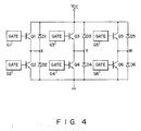
- Transistor circuits in the first and second regions A and B constitute gate circuits G1 and G2, respectively in an equivalent circuit diagram shown in Figure 4. Therefore, a terminal P1, which connects in common the P+ type separation layer 42a in the first region A to the N+ type layers 22 and 26 for separating the layer A from the layer B, acts as a reference voltage terminal the voltage potential of which changes within a range defined between 0 volts and a power source voltage Vcc.
- a terminal P2 that is connected to the P+ type separation layer 42b in the second region B functions as a fixed ground potential terminal.
- the N- type RESURF layer 25 has a dose of about 5 ⁇ 1011/cm2 to 3 ⁇ 1012/cm2.
- the value of specific resistance of the N- type epitaxial layer 24 serving as an elements-formation region is determined based on the characteristics of the transistors Q1 and Q2; it may range from 1 to 20 ohm-cm.
- This enables the gate circuits G1 and G2 for controlling and driving a transistor circuit module in Figure 4 to be formed on a "single chip" independently of other circuits.
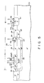
- a semiconductor device in accordance with the second embodiment of the present invention is generally designated by reference numeral "50" in Figure 5.
- a high-voltage MOSFET and its control gate circuitry are integrally formed together using the epitaxial semiconductor wafer in Figure 1.
- a gate circuit is formed in a first region A using a plurality of transistors separated from each other by PN junction separation.
- a high-voltage MOSFET is formed in a second region B.
- the high-voltage MOSFET is formed of a P type base layer 51 serving as a channel layer, an N type source layer 52 formed in the layer 51, a gate electrode layer 54 insulatively disposed above the P type base layer 51 by a gate insulating layer 53, a conductive source electrode layer 55 electrically contacting the source layer 52 and the P type base layer 51, and a conductive drain electrode layer 56 electrically contacting an N+ type diffusion layer 26.
- this embodiment when the voltage potential of the drain electrode 56 is varied in response to a turn-ON/OFF operation of the MOSFET, a gate circuit formed in the first region A is entirely changed without any influence to the circuitry in the second region B and can perform a desired circuit operation.
- this embodiment device may be also fabricated using the manufacturing process described with reference to Figures 2A through 2D.
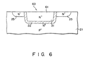
- a semiconductor device 60 in accordance with the third embodiment of the present invention is shown in Figure 6.
- This embodiment can be considered as an application of the second embodiment.
- a groove 23 is formed in a P- type silicon substrate 21.
- An N+ type diffusion layer 22 is formed on the inside surface of the groove 23.
- This groove 23 will be an elements-formation region.
- an N- type semiconductor layer 61 is deposited in the groove 23.
- An N-type RESURF layer 25 is then formed around this element region in the same manner as in the above-mentioned embodiments.
- a high-voltage semiconductor element or elements such as high-voltage MOSFET(s) and/or bipolar transistor(s) can be effectively formed in the N- type layer 61.
- an epitaxial semiconductor wafer according to the fourth embodiment of the present invention is generally designated by reference numeral "70.”
- a P+ type silicon substrate 21-1 is prepared on which an N- type silicon layer 21-2 is stacked, thereby to constitute an N- type silicon substrate 21.
- a P-type epitaxial layer 23 is formed on the silicon substrate 21.
- An N- type epitaxial layer 24 prospectively serving as an elements formation layer is formed on the P- type epitaxial layer 23.
- the substrate surface is divided into three regions A, B, and C, each of which is an elements-formation region in which one or a plurality of elements should be formed.
- Separating regions D are formed between the elements formation regions A, B, and C.
- N- type epitaxial layers laid 24 in the elements-formation regions A, B, and C are electrically separated from each other using P+ type diffusing layers 71 by PN junction-separation.
- P+ type diffusing layers 71 are formed to have a sufficient depth from the top surface of the wafer to reach the underlying P- type epitaxial layer 23 in the separation regions D.
- an N+ type semiconductor layer 22 is formed as a first element separation layer and is buried between the P- type epitaxial layer 23 and the substrate 21.
- N+ type diffusing layers 26 each having a depth from the wafer surface to reach the corresponding N+ type layers 22 are formed around the first regions A and B.
- the N+ type diffusion layer 26 serve as second element separation layers.
- An N- type layer 25 shown in Figure 7 is formed outside each of the N+ type layers 26.
- each of the element regions A, B, and C has the "N-/P-" type junction separation structure.
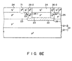
- a method of manufacturing the epitaxial wafer 70 will be described hereinafter with reference to Figures 8A through 8E, wherein the regions B, C, and D in Figure 7 are illustrated.
- an N+ type layer 22 having a selected high impurity concentration is formed by diffusion on the top surface of a silicon substrate 21 having a stacked structure consisting of layers 21-1 and 21-2.
- a P- type epitaxial layer 23 is formed on the entire surface of the substrate 21.
- an N type RESURF layer 25 is formed by ion implantation on the substrate 11 around an elements-formation region in which the N+ type layer 22 is formed, and an N+ type layer 26-1 for surrounding the element region together with the N+ type layer 22 is formed.
- the N+ type layer 26 is formed to have a depth to reach the N+ type layer 22, thereby defining a layer portion 23 separated by PN junction-separation.
- an N- type epitaxial layer 24 is grown to cover the entire top surface of the resultant wafer.
- a further N+ type layer 26-2 is formed by diffusion to just overlap the N+ type layer 26-1, thereby defining the N- type layer section 24 inside the N+ type layer 26-2.
- a P+ type layer 71 is formed by diffusion each separation region between these elements-formation regions. The P+ type layer 71 is formed to have a depth to reach and contact the underlying P- type layer 23.
- the stacked N+ type diffusing layers 26-1 and 26-2 serving as elements-separation layers together with the n+-type buried layers 22 in the elements-formation regions A and B are respectively formed in two diffusion steps, but these N+ type layers 26-1 and 26-2 can be modified to be formed together in only one diffusion step in the process.
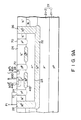
- Figures 9A and 9B show the main sectional structures of samples of IC devices obtained by integrally forming a plurality of transistors in elements-formation regions of the epitaxial wafer 70 in Figure 7.
- Figures 9A and 9B two of the plurality of elements-formation regions of the epitaxial wafer 70 are shown: Figure 9A shows a first region B surrounded by an N+ type layer 26; whereas Figure 9B shows a second region C located outside the first region B.
- One transistor is typically formed in each of the illustrated regions.
- N+ type collector buried layer 41 is formed in each of the regions B and C before an N- type epitaxial layer 24 is formed. (The N+ type collector buried layer 41 is omitted in the embodiment in Figure 7.)
- a P+ type layer 71 is formed in the second region C simultaneously with formation of a P+ type layer 71 for PN junction-separation from the first region B, and a P+ type layer 72 for separating elements from each other is formed in the first region B.
- a P type base layer 43, an N type emitter layer 44, and a collector take-out layer 45 are formed in a region surrounded by these layers 71 and 72, as shown in Figure 9A or 9B.
- the transistor circuit in the first region B constitutes a gate circuit G1 shown in Figure 4, for example; the transistor circuit in the second region C constitutes a gate circuit G2 shown in Fig 4, for instance.
- a terminal P1 for commonly connecting the N+ type layer 26 and the P+ type layer 71 serving as a separation layer for an inner region surrounded by the N+ type layer 26 is used as a reference voltage terminal having a voltage which changes within the range from 0 volts to the power source voltage Vcc.
- a terminal P2 connected to the P+ type separation layer 71 is used as a ground terminal to which a fixed ground potential is applied.
- NPN transistors are integrally formed
- the elements to be formed on the substrate may include other types of elements consisting of gate circuits such as CMOS transistors, diodes, resistors, capacitors, and so forth.
- CMOS transistors diodes
- resistors resistors
- capacitors and so forth.
- an epitaxial semiconductor wafer in accordance with the fifth embodiment of the present invention is generally designated by reference numeral "100".
- the wafer 100 differs from the above embodiment shown in Figure 7 in that an N- type epitaxial layer 24 is directly formed on a P- type silicon substrate 21 without forming a P type epitaxial layer.
- a P+ type layer 71 is formed in separation regions D for separating elements-formation regions A, B, C,... from each other.
- a P- type diffusion layer 101 is formed as an elements formation layer.
- an N- type layer 24 functions as an elements formation layer.
- the P- type layer 101 in the first region A or B is subdivided into a plurality of elements-formation sub regions by the N+ type layer 26.
- elements formation layers include N- and P- types layers of both conductivity types. Therefore, as detailed IC structures will be described later, element separation is performed by a P+ type layer in the N- type layer region; whereas, in the P- type layer region, the element separation is performed by an N+ type.
- a method of manufacturing the epitaxial semiconductor wafer 100 will be described below with reference to Figures 11A through 11D. These views of manufacturing steps show a range of the regions B, C, and D.
- an N+ type layer 22 serving as an elements-separation layer is formed by diffusion on a P- type silicon substrate 21. At this time, the N+ type layer 22 is formed in the region C as needed.
- an N- type epitaxial layer 24 is then formed on the entire top surface of the resultant substrate.
- a P+ type layers 71 for separating elements-formation regions from each other is formed by diffusion to have a depth to reach a substrate 21.
- the elements-formation regions A and B are separated from other regions.
- An N+ type layer 26 is formed on the elements-formation regions A and B to have a depth to reach the N+ type layer 22, thereby defining a plurality of element regions therein, as shown in Figure 11C.
- P- type layers 101 serving as elements-formation regions are formed by diffusion in the regions A and B.
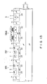
- Figure 12 shows a partial wafer structure according to the first region A (or B), whereas Figure 13 shows a partial wafer structure according to the second region C.
- a plurality of elements-formation regions formed in the first region A are separated by the N+ type layers 26 from each other.
- NPN transistors, PNP transistors, CMOS transistor circuits, and resistances are integrally formed.
- reference letters "PNP”, “NPN”, “CMOS”, and “R” are respectively added to these components for the sake of easy identification.
- the P- type layer 101 serving as an elements formation layer is formed to have a depth to reach the underlying N+ type layer 22.
- the resistor R is constituted by an N- type layer formed by diffusion on the P- type layer 101.
- the CMOS circuit is constituted by forming a P-channel MOSFET and an N-channel MOSFET in an N type well region and a P type well region formed in the P- type layer 101.
- An NPN transistor is a lateral transistor obtained by forming an emitter and a collector by diffusion and using the P- type layer 101 as a base of the NPN transistor.
- a PNP transistor is constituted by defining a conventional planar structure using the P-type layer 101 as a collector layer of the PNP transistor.
- a plurality of element regions in the second region C are separated from each other by P+ type layers 71 as shown in Figure 13.
- an NPN transistor, a PNP transistor, a CMOS transistor circuit, and a resistor R are integrally formed in each of the separated regions.
- a conductivity type of elements formation layers in the second region C is opposite to that in the first region A in the region C.
- the resistor R in Figure 13 is formed by a P type diffusion layer.
- the CMOS circuit is formed in the N type well region and the P type well region, as in the region A. Structures of the PNP transistor and the NPN transistor in the region C are opposite to those in the above region A; the PNP transistor has a lateral structure, and the NPN transistor has a planar structure.
- a transistor circuit formed in the region A of each of the wafers shown in Figure 12 and 13 is a gate circuit on a high voltage side, as in the previously presented embodiments; and a transistor formed in the region C is used as a gate circuit on a low voltage side.
- the N+ type layer 26 in Figure 12 is set to be the maximum voltage potential
- the reference voltage of the transistor circuit in the region A in Figure 12 can be desirably changed within the range between the ground potential (0 volts) and the power source voltage Vcc, independently of the reference voltage of the transistor circuit in the region C in Figure 12.
- gate circuits G1 to G6 for driving/controlling the transistor circuit module shown in Figure 4 can be effectively packaged in one chip.
- the P- type layer 101 is not always absolutely required, and, for example, the P- type layer 101 need not be formed in a region for forming a resistor.
- N+ type buried layers 22 in a PNP transistor-formation region or a CMOS circuit-formation region can be omitted depending on conditions.
Landscapes
- Element Separation (AREA)
- Bipolar Transistors (AREA)
- Metal-Oxide And Bipolar Metal-Oxide Semiconductor Integrated Circuits (AREA)
Applications Claiming Priority (6)
| Application Number | Priority Date | Filing Date | Title |
|---|---|---|---|
| JP25494289 | 1989-09-29 | ||
| JP25494289 | 1989-09-29 | ||
| JP254942/89 | 1989-09-29 | ||
| JP344316/89 | 1989-12-28 | ||
| JP1344316A JP2835116B2 (ja) | 1989-09-29 | 1989-12-28 | 電力用icおよびその製造方法 |
| JP34431689 | 1989-12-28 |
Publications (2)
| Publication Number | Publication Date |
|---|---|
| EP0420672A1 true EP0420672A1 (fr) | 1991-04-03 |
| EP0420672B1 EP0420672B1 (fr) | 2000-07-19 |
Family
ID=26541928
Family Applications (1)
| Application Number | Title | Priority Date | Filing Date |
|---|---|---|---|
| EP90310645A Expired - Lifetime EP0420672B1 (fr) | 1989-09-29 | 1990-09-28 | Structure pour substrat semi-conducteur utilisée dans un dispositif IC à haute puissance |
Country Status (4)
| Country | Link |
|---|---|
| US (1) | US5159427A (fr) |
| EP (1) | EP0420672B1 (fr) |
| JP (1) | JP2835116B2 (fr) |
| DE (1) | DE69033594T2 (fr) |
Cited By (7)
| Publication number | Priority date | Publication date | Assignee | Title |
|---|---|---|---|---|
| EP0780900A1 (fr) * | 1995-12-19 | 1997-06-25 | Consorzio per la Ricerca sulla Microelettronica nel Mezzogiorno - CoRiMMe | Dispositif semi-conducteur monolithique avec structure de bord et méthode de fabrication |
| EP0782194A3 (fr) * | 1995-12-30 | 1998-06-10 | Mitsubishi Denki Kabushiki Kaisha | Dispositif semi-conducteur d'isolement à haute tension de claquage et procédé de fabrication d'un tel dispositif |
| EP0915508A1 (fr) * | 1997-10-10 | 1999-05-12 | STMicroelectronics S.r.l. | Circuit intégré à isolation par jonction très efficace |
| EP0802567A3 (fr) * | 1996-04-15 | 2000-07-05 | Denso Corporation | Dispositif semi-conducteur et procédé de fabrication |
| DE19906384A1 (de) * | 1999-02-16 | 2000-08-24 | Siemens Ag | IGBT mit PN-Isolation |
| US6242787B1 (en) | 1995-11-15 | 2001-06-05 | Denso Corporation | Semiconductor device and manufacturing method thereof |
| US6831331B2 (en) | 1995-11-15 | 2004-12-14 | Denso Corporation | Power MOS transistor for absorbing surge current |
Families Citing this family (16)
| Publication number | Priority date | Publication date | Assignee | Title |
|---|---|---|---|---|
| US6462976B1 (en) | 1997-02-21 | 2002-10-08 | University Of Arkansas | Conversion of electrical energy from one form to another, and its management through multichip module structures |
| US7169272B2 (en) * | 1997-04-30 | 2007-01-30 | Board Of Trustees Of The University Of Arkansas | Microfabricated recessed disk microelectrodes: characterization in static and convective solutions |
| US7144486B1 (en) | 1997-04-30 | 2006-12-05 | Board Of Trustees Of The University Of Arkansas | Multilayer microcavity devices and methods |
| US6225673B1 (en) * | 1998-03-03 | 2001-05-01 | Texas Instruments Incorporated | Integrated circuit which minimizes parasitic action in a switching transistor pair |
| DE19844531B4 (de) * | 1998-09-29 | 2017-12-14 | Prema Semiconductor Gmbh | Verfahren zur Herstellung von Transistoren |
| DE10028008A1 (de) * | 2000-06-06 | 2001-12-13 | Bosch Gmbh Robert | Schutzvorrichtung gegen elektrostatische Entladungen |
| US7348183B2 (en) * | 2000-10-16 | 2008-03-25 | Board Of Trustees Of The University Of Arkansas | Self-contained microelectrochemical bioassay platforms and methods |
| US7456028B2 (en) | 2000-10-16 | 2008-11-25 | Board Of Trustees Of The University Of Arkansas, N.A. | Electrochemical method for detecting water born pathogens |
| US6887714B2 (en) | 2000-10-16 | 2005-05-03 | Board Of Trustees Of The University Of Arkansas, N.A. | Microvolume immunoabsorbant assays with amplified electrochemical detection |
| JP4508606B2 (ja) * | 2003-03-20 | 2010-07-21 | 株式会社リコー | 複数種類のウエルを備えた半導体装置の製造方法 |
| JP4775683B2 (ja) * | 2003-09-29 | 2011-09-21 | オンセミコンダクター・トレーディング・リミテッド | 半導体集積回路装置 |
| JP4775684B2 (ja) * | 2003-09-29 | 2011-09-21 | オンセミコンダクター・トレーディング・リミテッド | 半導体集積回路装置 |
| US7443009B2 (en) * | 2005-05-11 | 2008-10-28 | Micron Technology, Inc. | N well implants to separate blocks in a flash memory device |
| JP5048242B2 (ja) * | 2005-11-30 | 2012-10-17 | オンセミコンダクター・トレーディング・リミテッド | 半導体装置及びその製造方法 |
| KR101063690B1 (ko) * | 2008-11-21 | 2011-09-14 | 주식회사 동부하이텍 | 반도체 소자 및 그 제조 방법 |
| JP5459403B2 (ja) * | 2011-03-28 | 2014-04-02 | トヨタ自動車株式会社 | 縦型半導体装置 |
Citations (5)
| Publication number | Priority date | Publication date | Assignee | Title |
|---|---|---|---|---|
| FR2154786A1 (fr) * | 1971-09-30 | 1973-05-11 | Sony Corp | |
| FR2309040A1 (fr) * | 1975-04-22 | 1976-11-19 | Tokyo Shibaura Electric Co | Circuit integre comportant un transistor vertical a base epitaxiale |
| EP0117867A1 (fr) * | 1982-08-26 | 1984-09-12 | Mitsubishi Denki Kabushiki Kaisha | Arrangement de semi-conducteur |
| EP0156964A1 (fr) * | 1983-11-18 | 1985-10-09 | Motorola, Inc. | Moyen et procédé pour isolation par jonction PN |
| GB2175138A (en) * | 1985-05-09 | 1986-11-19 | Sgs Microelettronica Spa | Bipolar integrated circuits |
Family Cites Families (3)
| Publication number | Priority date | Publication date | Assignee | Title |
|---|---|---|---|---|
| IT1214806B (it) * | 1984-09-21 | 1990-01-18 | Ates Componenti Elettron | Dispositivo integrato monolitico di potenza e semiconduttore |
| JPS63198367A (ja) * | 1987-02-13 | 1988-08-17 | Toshiba Corp | 半導体装置 |
| IT1215792B (it) * | 1988-02-04 | 1990-02-22 | Sgs Thomson Microelectronics | Transistore di tipo pnp verticale a collettore isolato con dispositivo per eliminare l'effetto di componenti parassiti di giunzione. |
-
1989
- 1989-12-28 JP JP1344316A patent/JP2835116B2/ja not_active Expired - Lifetime
-
1990
- 1990-09-26 US US07/588,544 patent/US5159427A/en not_active Expired - Lifetime
- 1990-09-28 DE DE69033594T patent/DE69033594T2/de not_active Expired - Fee Related
- 1990-09-28 EP EP90310645A patent/EP0420672B1/fr not_active Expired - Lifetime
Patent Citations (5)
| Publication number | Priority date | Publication date | Assignee | Title |
|---|---|---|---|---|
| FR2154786A1 (fr) * | 1971-09-30 | 1973-05-11 | Sony Corp | |
| FR2309040A1 (fr) * | 1975-04-22 | 1976-11-19 | Tokyo Shibaura Electric Co | Circuit integre comportant un transistor vertical a base epitaxiale |
| EP0117867A1 (fr) * | 1982-08-26 | 1984-09-12 | Mitsubishi Denki Kabushiki Kaisha | Arrangement de semi-conducteur |
| EP0156964A1 (fr) * | 1983-11-18 | 1985-10-09 | Motorola, Inc. | Moyen et procédé pour isolation par jonction PN |
| GB2175138A (en) * | 1985-05-09 | 1986-11-19 | Sgs Microelettronica Spa | Bipolar integrated circuits |
Non-Patent Citations (2)
| Title |
|---|
| IEDM 1984, San Francisco, 9th - 12th December 1984, pages 698-701, IEDM; T. OKABE et al.: "180V Analog-compatible high-speed logic utilizing semi-well isolation technology" * |
| L'ONDE ELECTRIQUE, vol. 67, no. 6, November 1987, pages 58-69, Paris, FR; P. ROSSEL: "M.O.S. technologies for smart power and high-voltage circuits" * |
Cited By (11)
| Publication number | Priority date | Publication date | Assignee | Title |
|---|---|---|---|---|
| US6242787B1 (en) | 1995-11-15 | 2001-06-05 | Denso Corporation | Semiconductor device and manufacturing method thereof |
| US6831331B2 (en) | 1995-11-15 | 2004-12-14 | Denso Corporation | Power MOS transistor for absorbing surge current |
| EP0780900A1 (fr) * | 1995-12-19 | 1997-06-25 | Consorzio per la Ricerca sulla Microelettronica nel Mezzogiorno - CoRiMMe | Dispositif semi-conducteur monolithique avec structure de bord et méthode de fabrication |
| US5830783A (en) * | 1995-12-19 | 1998-11-03 | Consorzio Per La Ricerca Sulla Microeletrronica Nel Mezzogiorno | Monolithic semiconductor device having an edge structure and method for producing said structure |
| EP0782194A3 (fr) * | 1995-12-30 | 1998-06-10 | Mitsubishi Denki Kabushiki Kaisha | Dispositif semi-conducteur d'isolement à haute tension de claquage et procédé de fabrication d'un tel dispositif |
| US6376891B1 (en) | 1995-12-30 | 2002-04-23 | Mitsubishi Denki Kabushiki Kaisha | High voltage breakdown isolation semiconductor device and manufacturing process for making the device |
| US6596575B2 (en) | 1995-12-30 | 2003-07-22 | Mitsubishi Denki Kabushiki Kaisha | High voltage breakdown isolation semiconductor device and manufacturing process for making the device |
| EP0802567A3 (fr) * | 1996-04-15 | 2000-07-05 | Denso Corporation | Dispositif semi-conducteur et procédé de fabrication |
| EP0915508A1 (fr) * | 1997-10-10 | 1999-05-12 | STMicroelectronics S.r.l. | Circuit intégré à isolation par jonction très efficace |
| DE19906384A1 (de) * | 1999-02-16 | 2000-08-24 | Siemens Ag | IGBT mit PN-Isolation |
| US6914270B2 (en) | 1999-02-16 | 2005-07-05 | Infineon Technologies Ag | IGBT with PN insulation and production method |
Also Published As
| Publication number | Publication date |
|---|---|
| DE69033594T2 (de) | 2001-03-15 |
| JPH03174741A (ja) | 1991-07-29 |
| EP0420672B1 (fr) | 2000-07-19 |
| DE69033594D1 (de) | 2000-08-24 |
| US5159427A (en) | 1992-10-27 |
| JP2835116B2 (ja) | 1998-12-14 |
Similar Documents
| Publication | Publication Date | Title |
|---|---|---|
| EP0420672A1 (fr) | Structure pour substrat semi-conducteur utilisée dans un dispositif IC à haute puissance | |
| US4862233A (en) | Integrated circuit device having vertical MOS provided with Zener diode | |
| US20020079554A1 (en) | Semiconductor integrated circuit device and manufacturing method thereof | |
| US6570229B1 (en) | Semiconductor device | |
| KR100208632B1 (ko) | 반도체 집적 회로 및 그 제조 방법 | |
| JPH07193154A (ja) | 半導体集積デバイス | |
| US20020079555A1 (en) | Semiconductor integrated circuit device and manufacturing method thereof | |
| US7888226B2 (en) | Method of fabricating power semiconductor device for suppressing substrate recirculation current | |
| KR100334381B1 (ko) | 유도성부하소자용집적드라이버회로 | |
| US7718481B2 (en) | Semiconductor structure and method of manufacture | |
| US5031019A (en) | Method for manufacturing a semiconductor device having isolated islands and its resulting structure | |
| US4829344A (en) | Electronic semiconductor device for protecting integrated circuits against electrostatic discharges | |
| EP0449093B1 (fr) | Dispositif de circuit pour prévenir les phénomènes de verrouillage dans des transistors PNP verticaux à collecteurs isolés | |
| US6127723A (en) | Integrated device in an emitter-switching configuration | |
| EP0381139B1 (fr) | Dispositif intégré à semi-conducteur et son procédé de fabrication | |
| US20050056907A1 (en) | Power transistor and semiconductor integrated circuit using the same | |
| US6441446B1 (en) | Device with integrated bipolar and MOSFET transistors in an emitter switching configuration | |
| JPH0342866A (ja) | 半導体装置及びその製造方法 | |
| JPS6060753A (ja) | 半導体装置 | |
| JPH0644626B2 (ja) | モノリシック半導体装置 | |
| KR0145119B1 (ko) | 다링톤 접속 반도체소자 및 그의 제조방법 | |
| KR100278424B1 (ko) | 높은 항복 전압을 지닌 얇은 능동층의 반도체 장치 | |
| US5830783A (en) | Monolithic semiconductor device having an edge structure and method for producing said structure | |
| JPH02283070A (ja) | 入力保護回路を備えた半導体集積回路装置 | |
| KR100216734B1 (ko) | 애노드 공통 병렬 사이리스터 및 사이리스터 모듈 제조방법 |
Legal Events
| Date | Code | Title | Description |
|---|---|---|---|
| PUAI | Public reference made under article 153(3) epc to a published international application that has entered the european phase |
Free format text: ORIGINAL CODE: 0009012 |
|
| 17P | Request for examination filed |
Effective date: 19901012 |
|
| AK | Designated contracting states |
Kind code of ref document: A1 Designated state(s): DE IT |
|
| 17Q | First examination report despatched |
Effective date: 19921023 |
|
| GRAG | Despatch of communication of intention to grant |
Free format text: ORIGINAL CODE: EPIDOS AGRA |
|
| GRAG | Despatch of communication of intention to grant |
Free format text: ORIGINAL CODE: EPIDOS AGRA |
|
| GRAH | Despatch of communication of intention to grant a patent |
Free format text: ORIGINAL CODE: EPIDOS IGRA |
|
| GRAH | Despatch of communication of intention to grant a patent |
Free format text: ORIGINAL CODE: EPIDOS IGRA |
|
| GRAA | (expected) grant |
Free format text: ORIGINAL CODE: 0009210 |
|
| AK | Designated contracting states |
Kind code of ref document: B1 Designated state(s): DE IT |
|
| ITF | It: translation for a ep patent filed | ||
| REF | Corresponds to: |
Ref document number: 69033594 Country of ref document: DE Date of ref document: 20000824 |
|
| EN | Fr: translation not filed | ||
| PLBE | No opposition filed within time limit |
Free format text: ORIGINAL CODE: 0009261 |
|
| STAA | Information on the status of an ep patent application or granted ep patent |
Free format text: STATUS: NO OPPOSITION FILED WITHIN TIME LIMIT |
|
| 26N | No opposition filed | ||
| PGFP | Annual fee paid to national office [announced via postgrant information from national office to epo] |
Ref country code: DE Payment date: 20070920 Year of fee payment: 18 |
|
| PGFP | Annual fee paid to national office [announced via postgrant information from national office to epo] |
Ref country code: IT Payment date: 20070926 Year of fee payment: 18 |
|
| PG25 | Lapsed in a contracting state [announced via postgrant information from national office to epo] |
Ref country code: IT Free format text: LAPSE BECAUSE OF NON-PAYMENT OF DUE FEES Effective date: 20080928 Ref country code: DE Free format text: LAPSE BECAUSE OF NON-PAYMENT OF DUE FEES Effective date: 20090401 |