EP0420700B1 - Appareil d'exposition - Google Patents
Appareil d'exposition Download PDFInfo
- Publication number
- EP0420700B1 EP0420700B1 EP90310709A EP90310709A EP0420700B1 EP 0420700 B1 EP0420700 B1 EP 0420700B1 EP 90310709 A EP90310709 A EP 90310709A EP 90310709 A EP90310709 A EP 90310709A EP 0420700 B1 EP0420700 B1 EP 0420700B1
- Authority
- EP
- European Patent Office
- Prior art keywords
- mask
- stage
- wafer
- alignment
- mark
- Prior art date
- Legal status (The legal status is an assumption and is not a legal conclusion. Google has not performed a legal analysis and makes no representation as to the accuracy of the status listed.)
- Expired - Lifetime
Links
- 238000012937 correction Methods 0.000 claims description 18
- 238000000034 method Methods 0.000 claims description 17
- 238000005259 measurement Methods 0.000 claims description 14
- 239000004065 semiconductor Substances 0.000 claims description 12
- 238000012546 transfer Methods 0.000 claims description 9
- 238000001514 detection method Methods 0.000 claims description 3
- 230000005855 radiation Effects 0.000 claims description 3
- 238000004519 manufacturing process Methods 0.000 claims description 2
- 239000000758 substrate Substances 0.000 description 11
- 238000012545 processing Methods 0.000 description 7
- 238000004891 communication Methods 0.000 description 6
- 230000003287 optical effect Effects 0.000 description 4
- 230000008569 process Effects 0.000 description 2
- 230000002411 adverse Effects 0.000 description 1
- 238000004378 air conditioning Methods 0.000 description 1
- 230000004075 alteration Effects 0.000 description 1
- 230000008859 change Effects 0.000 description 1
- 238000013461 design Methods 0.000 description 1
- 238000010586 diagram Methods 0.000 description 1
- 238000006073 displacement reaction Methods 0.000 description 1
- 230000000694 effects Effects 0.000 description 1
- 230000004907 flux Effects 0.000 description 1
- PCHJSUWPFVWCPO-UHFFFAOYSA-N gold Chemical compound [Au] PCHJSUWPFVWCPO-UHFFFAOYSA-N 0.000 description 1
- 239000010931 gold Substances 0.000 description 1
- 229910052737 gold Inorganic materials 0.000 description 1
- 238000012986 modification Methods 0.000 description 1
- 230000004048 modification Effects 0.000 description 1
- 230000001131 transforming effect Effects 0.000 description 1
Images



Classifications
-
- G—PHYSICS
- G03—PHOTOGRAPHY; CINEMATOGRAPHY; ANALOGOUS TECHNIQUES USING WAVES OTHER THAN OPTICAL WAVES; ELECTROGRAPHY; HOLOGRAPHY
- G03F—PHOTOMECHANICAL PRODUCTION OF TEXTURED OR PATTERNED SURFACES, e.g. FOR PRINTING, FOR PROCESSING OF SEMICONDUCTOR DEVICES; MATERIALS THEREFOR; ORIGINALS THEREFOR; APPARATUS SPECIALLY ADAPTED THEREFOR
- G03F7/00—Photomechanical, e.g. photolithographic, production of textured or patterned surfaces, e.g. printing surfaces; Materials therefor, e.g. comprising photoresists; Apparatus specially adapted therefor
- G03F7/70—Microphotolithographic exposure; Apparatus therefor
- G03F7/708—Construction of apparatus, e.g. environment aspects, hygiene aspects or materials
- G03F7/70858—Environment aspects, e.g. pressure of beam-path gas, temperature
- G03F7/70883—Environment aspects, e.g. pressure of beam-path gas, temperature of optical system
-
- G—PHYSICS
- G03—PHOTOGRAPHY; CINEMATOGRAPHY; ANALOGOUS TECHNIQUES USING WAVES OTHER THAN OPTICAL WAVES; ELECTROGRAPHY; HOLOGRAPHY
- G03F—PHOTOMECHANICAL PRODUCTION OF TEXTURED OR PATTERNED SURFACES, e.g. FOR PRINTING, FOR PROCESSING OF SEMICONDUCTOR DEVICES; MATERIALS THEREFOR; ORIGINALS THEREFOR; APPARATUS SPECIALLY ADAPTED THEREFOR
- G03F9/00—Registration or positioning of originals, masks, frames, photographic sheets or textured or patterned surfaces, e.g. automatically
- G03F9/70—Registration or positioning of originals, masks, frames, photographic sheets or textured or patterned surfaces, e.g. automatically for microlithography
Definitions
- This invention relates to an exposure apparatus for exposing a substrate such as a semiconductor wafer to an original such as a mask, wherein the original and the substrate are disposed opposed to each other.
- US-A-4 801 208 discloses the alignment of a mask with a substrate in which plural exposure areas of the substrate are exposed by light of a predetermined wavelength, which is also used for alignment purposes to reduce alignment error due to aberration of a projection optical system.
- a pattern transfer method usable with a mask (2) having a transfer pattern (418) and a plurality of alignment marks (420, 421), and with a wafer (3), for lithographically transferring the transfer pattern of the mask (2) to the wafer (3) comprising the steps of providing a reference mark (14) on a wafer stage (24), mounting the mask (2) on a mask stage (4), mounting the wafer (3) on the wafer stage (24) having a predetermined stage coordinate system, and aligning the mask (2) and the wafer (3) relative to each other, which includes the steps of:
- an X-Y stage for moving the substrate, to be exposed is provided with a mark for alignment of the original. Any positional deviation between such mark on the X-Y stage and a plurality of alignment marks provided on the original, is measured. The position of the original is adjusted with respect to the coordinate system of the X-Y stage, on the basis of the position coordinate of the alignment marks of the original in respect of the X-Y stage coordinate.
- the original aligning mark on the X-Y stage is formed at a particular location, and the X-Y stage is moved sequentially so that the mark of the X-Y stage is sequentially placed at the positions below the alignment marks of the original, respectively.
- the amount of deviation between the mark of the X-Y stage and each mark of the original is measured to determine the X-Y coordinate of each alignment mark of the original.
- the ⁇ component is corrected by moving the stage for the original.
- the amount of correction in the X and Y components is fed back, as a corrective quantity for the position coordinate of each shot area when the pattern of the original is to be printed on that shot area of the substrate.
- the alignment operation for the original includes a step of rough alignment only in regard to the ⁇ component, using two of marks provided on the original, and a step of final alignment in regard to the X, Y and ⁇ components, using two or more marks.
- the alignment of the original is executed with respect to the coordinate system of the main body of the exposure apparatus. This leads to that, if there is an error between the coordinate system of the substrate stage and the coordinate system of the main body of the apparatus, an error is produced between the direction of movement of the substrate stage and the direction of corrective drive as calculated from the deviation between the original and the substrate. Such an error adversely affects the alignment precision.
- the original is aligned with respect to the coordinate system of the stage.
- the precision of relative position of the original and the substrate, to be exposed can be improved.
- the effect of an error between the coordinate system of the substrate stage and the coordinate system of the main body of the apparatus, upon the alignment precision, is reduced, such that the assembling and adjustment of the main body of the apparatus and the stage coordinate is easier.
- the alignment of the original is executed by two steps of rough alignment in respect to the ⁇ component and final or fine alignment in respect to the X, Y bind ⁇ components. This is effective to reduce the number of times of searching operation and, thus, effective to improve the throughput.
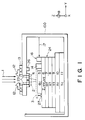
- Figure 1 illustrates the structure of a part of a step-and-repeat type exposure apparatus (stepper) which pertains to the mask-to-wafer alignment and which is around an exposure stage.
- stepper step-and-repeat type exposure apparatus
- denoted at 1 is light for exposure (photoprinting) which is projected substantially along the Z-axis direction and which comprises X-rays contained in a synchrotron orbit radiation (SOR), for example.
- SOR synchrotron orbit radiation
- Denoted at 2 is a mask having formed thereon a pattern which is to be transferred onto a semiconductor wafer 3.
- Denoted at 4 is a mask ⁇ stage for rotationally moving the mask 2 along a plane (X-Y plane) parallel to the surface thereof; and at 5 is a ⁇ rough-motion stage for rotationally moving the wafer 3 along a plane (X-Y plane) parallel to the surface thereof.
- Denoted at 6 is a Z tilt stage which is effective to move the wafer 3 in the Z direction (movement toward the exposure light 1), in the wx direction (rotation about the X axis) and in the wy (rotation about the Y axis), respectively, when the wafer 3 is to be opposed to the mask 2 with a predetermined proximity gap in the Z-axis direction.
- Denoted at 7 is a ⁇ fine-motion stage for minutely rotating the wafer 3 in the X-Y plane; at 8 is an X fine-motion stage for minutely moving the wafer in the X direction; at 9 is a Y fine-motion stage for minutely moving the wafer in the Y direction; at 10 is an X rough-motion stage; and at 11 is a Y rough-motion stage.
- the ⁇ rough-motion stage 5, the Z tilt stage 6, the ⁇ fine-motion stage 7, the X fine-motion stage 8, the Y fine-motion stage 9, the X rough-motion stage 10 and the Y rough-motion stage 11, cooperate with each other to provide a wafer stage 24.
- Denoted at 12 are pickups which are adapted to project light to alignment marks formed on the mask 2 and the wafer 3 and which are adapted to detect scattered light from these marks.
- each alignment mark XU, XD, YL and YR are formed on scribe lines of each shot area of the wafer 3, each mark being disposed closed to an end of corresponding sides of that shot area.
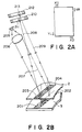
- Each alignment mark comprises a diffraction grating, as shown in Figure 2B, which provides an autoalignment (AA) mark 201 adapted to detect an error in the mask-to-wafer registration with respect to a direction which is parallel to the side at which that alignment mark is formed, as well as an autofocusing (AF) mark 202, for detection of the spacing between the mask 2 and the wafer 3.
- the alignment mark has been formed on the wafer together with a semiconductor circuit pattern, in the preceding process.
- the mask 2 is provided with four alignment marks (203, 204) associated with the alignment marks of the wafer 3, respectively, which mask alignment marks are formed of gold, for example, together with a semiconductor circuit pattern which is to be transferred to the wafer (see Figure 10A).
- 205 is a semiconductor laser (light emitting element); at 206 is a collimator lens for transforming the light emitted by the semiconductor laser 205 into a parallel light; at 207 is the light beam emitted by the semiconductor laser 205 and transformed by the collimator lens 206 into the parallel light; at 208 is an autoalignment (AA) light beam, to be received, which bears positional deviation information (AA information) given by an optical system constituted by the AA mark 201 of the wafer and the AA mark 203 of the mask; and at 209 is an autofocusing (AF) light beam, to be received, which bears gap information (AF information) given by an optical system constituted by the AF mark 202 of the wafer and the AF mark 204 of the mask.
- AA autoalignment
- AF autofocusing
- Denoted at 210 is an autoalignment (AA) sensor for converting the position of an autoalignment (AA) light spot 211, formed by the AA light beam 208, into an electric signal (AA information).
- the sensor 210 comprises a line sensor such as a CCD array.
- Denoted at 212 is an autofocusing (AF) sensor for converting the position of an autofocusing (AF) light spot 213, formed by the AF light beam 209, into an electric signal (AF information).
- the sensor 212 comprises a line sensor such as a CCD array.
- denoted at 14 is a mask aligning reference mark provided on the wafer stage 24 for alignment between the mask 2 and the wafer stage 24.
- This reference mark 14 comprises four mark elements corresponding to the four alignment marks provided on the mask 2.
- Denoted at 16 is a super flat mirror; and at 17 is a Y-measurement beam and ⁇ -measurement beam which is projected to and reflected by the mirror 16, for measurement of the amount of displacement of the wafer stage 24 in the Y direction as well as the inclination ⁇ thereof about the Z axis.
- the position (X, Y, ⁇ ) of the wafer stage 24 with respect to the stage coordinate system can be measured through an interferometer.
- Denoted at 100 is a main body frame to which the mask ⁇ stage 4 and the wafer stage 24 as well as the pickups 12 are mounted.
- Figure 3 illustrates the structure of a control system of the exposure apparatus of Figure 1. While not shown in the drawings, the exposure apparatus of Figure 1 is equipped with a mirror unit for expanding the flux of X-rays, emitted from a SOR in the form of a horizontal sheet-like beam, in the vertical direction to provide an area beam; a main part unit which includes an alignment unit for aligning the mask and the wafer and an exposure unit for exposing the aligned mask and the wafer with the area X-ray beam; an attitude control unit for controlling the attitude of each of the mirror unit and the main-part unit; as well as a chamber and air conditioning unit for controlling the ambience around the mirror unit and the main-part unit.
- a mirror unit for expanding the flux of X-rays, emitted from a SOR in the form of a horizontal sheet-like beam, in the vertical direction to provide an area beam
- a main part unit which includes an alignment unit for aligning the mask and the wafer and an exposure unit for exposing the aligned mask and the wafer with the
- 301 is a main processor unit for controlling the operation of the apparatus as a whole; at 302 is a communication line for communicating the main processor unit 301 with the main-part unit; at 303 is a main-part side communication interface; at 304 is a main-part control unit; and at 305 is a pickup stage control means.
- Denoted at 306 and 308 are communication interfaces and denoted at 307 is a communication line, all of which are adapted to communicate, in the main-part unit, the main-part control unit 304 with fine AA/AF control means 309a, 309b, 309c and 309d for measurement of mark positional deviation for the purpose of mask alignment and mask-to-wafer alignment.
- Denoted at 310 and 312 are communication interfaces and denoted at 311 is a communication line all of which are adapted to communicate, in the main-part unit, the main-part control unit 304 with a stage control means 313 which controls the alignment corrective drive and the stepwise movement.
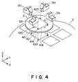
- Figure 4 illustrates the step-and-repeat exposure method.
- the mask ⁇ stage 4 which is driving means for the mask 2
- the wafer stage 24 which is driving means for the wafer 3
- the pickup stage 13 which is driving means for the pickup 12
- FIG 4 denoted at 12 (12a - 12d) are pickups for aligning the mask 2 and the wafer 3; at 418 is a pattern (to be transferred) formed on the mask; at 419 is a pattern, transferred, having been formed on the wafer in the preceding process; at 420 are alignment marks for mask alignment, to be used for aligning the mask 2 with a reference mark 14 ( Figure 1) provided on the wafer stage 24; at 421 are alignment marks formed on the mask, for aligning the mask pattern 418 with the transferred pattern 419; at 422 are alignment marks formed on the wafer for the same purpose; at 423 are projected light beams, projected from the pickups 12 for the same purpose; and at 401 are scribe lines defined between shot areas. The alignment marks 421 and 422 of the mask and the wafer are formed on these scribe lines.
- the alignment marks 420 on the mask there are four marks which are provided at the middles of the four sides of the mask pattern 418, corresponding to the scribe lines 401 of the wafer defined between adjacent shot areas.
- the mask marks 420 for exclusive use of alignment may be omitted and the alignment marks 421 of the mask for the mask-to-wafer alignment may be used also for the mask alignment.
- the mask 2 can be aligned with the coordinate system (stage coordinate system) of the wafer stage 24 in the following manner: First, the wafer stage 24 is moved successively to place, in sequence, the alignment reference mark 14 of the wafer stage 24 at a position (measuring position) aligned with each mask mark 420 (or 421), and each time the wafer stage 24 is positioned the light beam 423 is projected from corresponding pickup 12 (12a - 12d) having been moved to the corresponding mask mark, to measure relative positional deviation between the reference mark 14 and the corresponding mask mark in respect to the X and Y directions.
- stage coordinate system stage coordinate system
- the mask 2 and the wafer 3 can be aligned with each other in the following manner: First, under the condition that the mask 2 and the wafer 3 are supported to be opposed to each other, the pickups 12a - 12d project light beams 423 and, through the corresponding alignment marks 421 and 422 of the mask and the wafer, the gap between the mask and the wafer is measured. On the basis of the information obtained from the four pickups, the amount of gap correcting drive is calculated and the wafer stage 24 is driven to set the gap between the mask and the wafer in respect to the z-axis direction, to be equal to the gap for exposure.
- the pickups 12a - 12d project light beams 423 again, and deviation between paired alignment marks 421 and 422 of the mask and the wafer, along a plane parallel to the surface of the mask or wafer, is measured.
- the amount of corrective drive of that shot area as a whole is calculated, and the mask ⁇ stage 4 and the wafer stage 24 are driven to bring the mask pattern 418 and the wafer pattern 419 into alignment with each other.
- the exposure operation is effected, whereby the mask pattern 418 is transferred onto the wafer 3.
- the wafer stage 24 is driven so that the next shot area comes to a position below the mask.
- the alignment and exposure operation is repeated, whereby exposures of all the shot areas are effected.
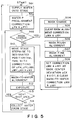
- Figure 5 is a flow chart, illustrating the flow of the step-and-repeat exposure sequence.
- a wafer is supplied to the wafer stage 24, and the supplied wafer is held on the wafer stage 24.
- the wafer stage 24 is moved and two alignment marks of the wafer 2 are measured through a prealignment optical system (not shown), and the prealignment of the wafer 2 is executed.
- the prealignment correction quantities ⁇ Px and ⁇ Py are memorized.
- step 503 discrimination is made as to the necessity of mask replacement. If the exposure is to he effected by using the mask which is being held at this time, the sequence goes to step 510. If the mask is to be replaced by another, the sequence goes to step 504.
- the current mask is demounted from the mask stage 4, by using a mask traverser (not shown) and the demounted mask is stored into a mask cassette (not shown). Then, a mask to be used for the exposure is taken out of its mask cassette by using the mask traverser and it is supplied to the mask stage 4.
- step 505 the mask alignment correction quantities ⁇ MX and ⁇ MY having been memorized in a memory, are cleared.
- mask rough alignment is effected by using two (YR and YL) of the four alignment marks 421 formed on the mask 2.
- Figure 6 illustrates details of the mask rough alignment operation.
- an alignment mark (reference mark 14) of the wafer stage 24 is used to measure the positional deviation ( ⁇ Xyr and ⁇ Yyr) of the mark YR of the mask alignment marks 421, with respect to the reference mark 14.
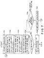
- Figure 7 illustrates details of the mask rough alignment mark measuring operation, made at step 601 of Figure 6.
- the quantities ⁇ Xm and ⁇ Ym of searching movement having been memorized in the memory are cleared.
- the pickup 12 for measurement of the mark YR (hereinafter, this pickup will be referred to as "YR pickup") is moved to the position which corresponds to the sum of the stage coordinate (Xyr, Yyr) of the mask YR mark 421, the mask alignment correction quantities ( ⁇ MX and ⁇ MY) and the searching movement quantities ( ⁇ Xm and ⁇ Ym).
- the stage coordinate means the design position coordinate or the position coordinate, actually measured by using a sample, in the stage coordinate system of the mask YR mark 421, for example, and the stage coordinate of each mark or each shot area is set prior to the exposure step.
- the wafer stage 24 is moved to place the alignment mark (reference mark) 14 thereof at the position which corresponds to the sum of the stage coordinate (Xyr, Yyr) of the mask YR mark 421, the mask alignment correction quantities ( ⁇ MX and ⁇ MY) and the searching movement quantities ( ⁇ Xm and ⁇ Ym).
- step 704 relative deviation ⁇ y between the mask YR mark 421 and the alignment mark 14 of the stage is measured through the YR pickup 12, and the sequence goes to step 705.
- step 705 discrimination is made as to whether the measurement of the deviation ⁇ y has been attained or not. If not, the sequence goes to step 706 whereat discrimination is made as to whether the measurement to all the points at the searching position has been completed or not. If not, the sequence goes to step 707 wherein the quantities ⁇ Xm and ⁇ Ym for the next searching movement are set. After this, the flow goes back to step 702, and the operations at step 702 and steps following it are repeated. If the result of discrimination at step 706 is affirmative, which means failure of the YR mark measurement, the sequence goes to an error routine, whereby the exposure processing is stopped or, alternatively, an alarm or display of error is provided.
- step 705 if the result of discrimination at step 705 is affirmative, the flow goes to step 708 wherein the quantities ⁇ Xm and ⁇ Y + ⁇ Ym are memorized as the positional deviation ( ⁇ Xyr and ⁇ Yyr) of the mask YR mark 421 and, thereafter, the mask rough alignment mark measuring operation is completed and the sequence goes to step 602 in Figure 6.
- positional deviation ( ⁇ Xyl and ⁇ Yyl) of the mask YL mark is measured in the same manner as at step 601, except for that the mark YL of the mask is used as the mask mark 421 and the YL pickup 12 is used as the corresponding pickup 12.
- the positional deviation ( ⁇ X, ⁇ Y and ⁇ ) of the mask 2 is calculated on the basis of the detected positional deviation quantities ⁇ Xyr and ⁇ Yyr of the mask YR mark and of the detected positional deviation quantities ⁇ Xyl and ⁇ Yyl of the mask YL mark.
- the mask ⁇ stage 4 is driven by an amount corresponding to the deviation ⁇ while, on the other hand, the determined positional deviation quantities ⁇ X and ⁇ Y are added to the mask alignment correction quantities ⁇ MX and ⁇ MY.
- the sequence goes to step 605 whereat discrimination is made as to whether the mask positional deviation ⁇ is within the tolerance of the rough alignment.
- step 606 the mask rough alignment operation counter is incremented and whether or not the counted number is beyond a preset number of retries, is discriminated. If the counted number is larger than the preset number, which means failure of mask ⁇ rough alignment in spite of retries of a predetermined number, the sequence goes to an error routine wherein the exposure processing is stopped or, alternatively, an alarm or display of error is provided. If the counted number is smaller than the set number of retries, the flow goes back to step 601 and the ⁇ rough alignment operation at step 601 and steps following it is retried.
- step 605 If the result of discrimination at step 605 is affirmative, the mask rough alignment operation is completed and the sequence goes to step 507 in Figure 5.
- the reference mark 14 of the wafer stage 24 and four alignment marks 421 (XU, XD, YL and YR) of the mask 2 are used to execute the mask fine alignment.
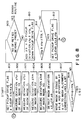
- Figure 8 illustrates details of the mask fine alignment operation.
- the pickup drive designation flag is set, and the quantities ⁇ Xp and ⁇ Yp of the pickup deviation are cleared.
- the alignment mark 14 of the wafer stage 24 is used to measure the positional deviation ⁇ Yyr of the mark YR which is one of the alignment marks 421 of the mask.
- Figure 9 illustrates details of the mask fine alignment mark measuring operation to be made at step 802 in Figure 8.
- step 901 the pickup drive designation flag is checked. If it has been set, at step 902 the YR pickup 12 is moved to the position which corresponds to the sum of the stage coordinate (Xyr, Yyr) of the mask YR mark 421 and the mask alignment correction quantities ⁇ MX and ⁇ MY having been memorized in the preceding operation. Then, the sequence goes to step 903. If, on the other hand, the pickup drive designation flag has not been set, the processing at step 902 is skipped, and the flow goes directly to step 903 from step 901.
- the wafer stage is moved to place the alignment mark 14 thereof at the position which corresponds to the sum of the stage coordinate (Xyr, Yyr) of the mask YR mark 421 and the mask alignment correction quantities ⁇ MX and ⁇ MY.
- positional deviation ⁇ y between the mask YR mark 421 and the alignment mark 14 of the stage is measured through the YR pickup 12.
- discrimination is made as to whether the measurement of the deviation ⁇ y has been attained or not. If not, which means failure of correct execution of the YR mark rough alignment operation (step 506 in Figure 5), the sequence goes to an error routine whereby the exposure processing is stopped or, alternatively, an alarm or display of error is provided.
- step 905 If the result of discrimination at step 905 is affirmative, then the flow goes to step 906 in which the quantity ⁇ y is set as the positional deviation ⁇ Yyr of the YR mark 421 and, after this, the mask fine alignment mark measuring processing is finished and the flow goes to step 803 in Figure 8.
- positional deviation ⁇ Yyl of the mask mark YL is measured in the same manner as at step 802, except for that the mask mark YL is used as the mask alignment mark 421 and the YL pickup is used as the pickup 12. Then, at step 804 and at step 805, in the same manner as at step 802 and at step 803, positional deviation ⁇ Xxu of the mask mark XU and positional deviation ⁇ Xxd of the mask mark XD are measured.
- the quantities ⁇ X, ⁇ Y and ⁇ of positional deviation of the mask 2 with respect to the X-Y coordinate system of the stage 24 are calculated on the basis of the detected positional deviation quantities ⁇ Yyr, ⁇ Yyl, ⁇ Xxu and ⁇ Xxd of the respective marks.
- the mask ⁇ stage 4 is driven by an amount corresponding to the positional deviation ⁇ while, on the other hand, the quantities ⁇ X and ⁇ Y are added to the mask alignment correction quantities MX and MY.
- the sequence goes to step 808 in which discrimination is made as to whether the mask positional deviation ( ⁇ X, ⁇ Y and ⁇ ) is within the tolerance for mask alignment or not.
- step 809 discrimination is made as to whether the number of times of the mask fine alignment operation is larger than a preset number of retries or not. If the result is affirmative, which means failure of mask fine alignment in spite of execution of a predetermined number of retries, the sequence goes to an error routine whereby the exposure processing is stopped, or alternatively, an alarm or display of error is provided. If the number is not larger than the set number of retries, the sequence goes to step 810 in which the positional deviation quantities ⁇ X and ⁇ Y are added to the pickup deviation quantities ⁇ Xp and ⁇ Yp, and the pickup drive designation flag is turned off.
- step 811 discrimination is made as to whether the pickup deviation ( ⁇ Xp and ⁇ Yp) is within the tolerance or not. If not, the flow goes to step 812 and the pickup drive designation flag is set, while the quantities ⁇ Xp and ⁇ Yp of the pickup deviation are cleared. After this, the flow goes back to step 802 and the operations at step 802 and steps following it are repeated. This ensures that, when the mask fine alignment mark measuring operation at steps 802, 803, 804 and 805 (details are illustrated in Figure 9) is subsequently to be executed, the pickup 12 is moved to catch the center of the mask mark 421. Thus, the precision of the mask fine alignment operation can be improved. If, on the other hand, the result of discrimination at step 811 is affirmative, the processing at step 812 is skipped and the flow goes directly back to step 802 from step 811.
- step 808 If the result of discrimination at step 808 is affirmative, the mask fine alignment operation is finished and the sequence goes to step 508 in Figure 5.
- the mask alignment correction quantities ⁇ MX and ⁇ MY are set as the quantities ⁇ CX and ⁇ CY of the mask center deviation, while the correction quantities ⁇ WX and ⁇ WY of the mask-to-wafer alignment are cleared.
- the flow goes to step 510.
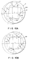
- the mask 2 having been set with deviation with respect to the stage coordinate system 1001 such as shown in Figure 10A, can be aligned with the stage coordinate system such as shown in Figure 10B.
- the wafer stage 24 is moved stepwise to the position having such coordinate as obtainable by correcting the preset coordinate (Xsn, Ysn) of the shot area in accordance with the prealignment correction quantities ⁇ PX and ⁇ PY, the mask alignment correction quantities ⁇ MX and ⁇ MY, and the mask-to-wafer alignment correction quantities ⁇ WX and ⁇ WY.
- the mask-to-wafer alignment is executed by using the wafer alignment marks 422 (YR, YL, XU and XD) and the mask alignment mark 421 (YR, YL, XU and XD).
- the correction quantities in the X and Y directions as assumed when the mask-to-wafer alignment is effected are equal to the quantities ⁇ WX and ⁇ WY, and these quantities change with the alignment operation to each shot area. After the subsequent exposure operation to the shot area at step 512, the flow goes to step 513.
- step 513 discrimination is made as to whether there remains an unexposed shot area on the same wafer. If it remains, the sequence goes back to step 503 and the above-described operations at step 503 and steps following it are repeated. If it does not remain, the sequence goes back to step 501, and after the wafer replacement, the above-described operations at step 502 and steps following it are repeated.
Landscapes
- Health & Medical Sciences (AREA)
- General Physics & Mathematics (AREA)
- Physics & Mathematics (AREA)
- Toxicology (AREA)
- Engineering & Computer Science (AREA)
- Environmental & Geological Engineering (AREA)
- Epidemiology (AREA)
- Public Health (AREA)
- Atmospheric Sciences (AREA)
- Life Sciences & Earth Sciences (AREA)
- Exposure And Positioning Against Photoresist Photosensitive Materials (AREA)
- Exposure Of Semiconductors, Excluding Electron Or Ion Beam Exposure (AREA)
- Control Of Position Or Direction (AREA)
Claims (10)
- Procédé de transfert de motif utilisable avec un masque (2) ayant un motif à transférer (418) et plusieurs repères d'alignement (420, 421), et avec une tranche (3), pour le transfert lithographique du motif à transférer du masque (2) à la tranche (3), le procédé comprenant les étapes de pose d'un repère de référence (14) sur une platine (24) pour tranche, de montage du masque (2) sur une platine (4) pour masque, de montage de la tranche (3) sur la platine (24) pour tranche ayant un système prédéterminé de coordonnées de platine, et d'alignement du masque (2) et de la tranche (3) l'un par rapport à l'autre, et de mesure de la relation positionnelle entre le repère de référence (14) situé sur la platine (24) pour tranche et les repères d'alignement (420, 421) du masque (2) afin de déterminer une erreur en rotation, dans une direction de rotation () du masque (2) par rapport au système de coordonnées de la platine (24) pour tranche ; caractérisé par l'étape de :réglage de la position du masque (2) en référence au système de coordonnées de platine sur la base de la mesure, par déplacement de la platine (4) pour masque dans la direction de rotation pour corriger l'erreur de rotation déterminée.
- Procédé selon la revendication 1, caractérisé en ce que la platine (24) pour tranche est montée sur un mécanisme à platine X-Y (8, 9, 10, 11).
- Procédé selon la revendication 1 ou 2, caractérisé par le montage du masque (2) sur une platine (4) pour masque ayant un mécanisme à platine à rotation ().
- Procédé selon la revendication 1, caractérisé par un déplacement séquentiel de la platine (24) pour tranche et l'exécution d'une mesure séquentielle de la relation positionnelle de chaque repère d'alignement (420, 421) avec le repère de référence (14).
- Procédé selon la revendication 4, caractérisé par l'exécution d'une action en retour du résultat de la mesure pour commander un mouvement de la platine (24) pour tranche pour l'opération de transfert de motif.
- Procédé selon la revendication 1, caractérisé par l'utilisation de deux des repères d'alignement (420, 421) pour exécuter un alignement dans l'alignement de la direction de rotation (), tandis qu'au moins deux des repères d'alignement (420, 421) sont utilisés pour exécuter un alignement dans les directions X, Y et .
- Procédé selon la revendication 6, caractérisé en ce que, lorsque l'erreur de rotation calculée est supérieure à une tolérance, le masque (2) est déplacé en rotation dans la direction d'une quantité ayant pour effet de corriger l'erreur de rotation et, ensuite, la détection d'erreurs de position des repères d'alignement (420, 421) est répétée, et dans lequel, lorsque l'erreur de rotation calculée n'est pas supérieure à la tolérance, le masque (2) est déplacé en rotation dans la direction d'une quantité ayant pour effet de corriger l'erreur de rotation, grâce à quoi une correction de la position en rotation de l'original est menée à bien.
- Procédé selon la revendication 7, caractérisé en ce que, lorsque l'erreur de rotation ne devient pas égale ou inférieure à la tolérance d'un nombre prédéterminé par suite de répétitions de la correction de la position en rotation du masque (2) sur la base d'une détection des erreurs de position des repères d'alignement (420, 421), la correction de la position en rotation du masque (2) est achevée.
- Procédé selon l'une quelconque des revendications précédentes, caractérisé par l'utilisation d'un rayonnement X pour le transfert lithographique.
- Procédé de fabrication d'un dispositif semiconducteur comprenant le procédé de transfert de motif selon l'une quelconque des revendications précédentes, l'étape d'exposition de la tranche (3) à un rayonnement X à travers le masque (2) pour former un motif de semiconducteur sur la tranche (3), et l'étape de fabrication d'un dispositif semiconducteur en utilisant la tranche exposée (3).
Applications Claiming Priority (3)
| Application Number | Priority Date | Filing Date | Title |
|---|---|---|---|
| JP252348/89 | 1989-09-29 | ||
| JP25234889 | 1989-09-29 | ||
| JP1252348A JP2829642B2 (ja) | 1989-09-29 | 1989-09-29 | 露光装置 |
Publications (4)
| Publication Number | Publication Date |
|---|---|
| EP0420700A2 EP0420700A2 (fr) | 1991-04-03 |
| EP0420700A3 EP0420700A3 (en) | 1992-01-02 |
| EP0420700B1 true EP0420700B1 (fr) | 2000-04-05 |
| EP0420700B8 EP0420700B8 (fr) | 2003-07-02 |
Family
ID=17236035
Family Applications (1)
| Application Number | Title | Priority Date | Filing Date |
|---|---|---|---|
| EP90310709A Expired - Lifetime EP0420700B8 (fr) | 1989-09-29 | 1990-09-28 | Appareil d'exposition |
Country Status (4)
| Country | Link |
|---|---|
| US (1) | US5142156A (fr) |
| EP (1) | EP0420700B8 (fr) |
| JP (1) | JP2829642B2 (fr) |
| DE (1) | DE69033499T2 (fr) |
Families Citing this family (38)
| Publication number | Priority date | Publication date | Assignee | Title |
|---|---|---|---|---|
| JP3168018B2 (ja) * | 1991-03-22 | 2001-05-21 | キヤノン株式会社 | 基板吸着保持方法 |
| JPH0540013A (ja) * | 1991-08-05 | 1993-02-19 | Canon Inc | ずれ測定方法及びこの方法を用いた露光装置 |
| US5329130A (en) * | 1991-08-06 | 1994-07-12 | Fujitsu Limited | Charged particle beam exposure method and apparatus |
| CA2078732A1 (fr) * | 1991-09-27 | 1993-03-28 | Koichi Sentoku | Dispositif de mesure des deplacements et methode de mesure des deplacements |
| JP3187093B2 (ja) * | 1991-09-27 | 2001-07-11 | キヤノン株式会社 | 位置ずれ測定装置 |
| US5495336A (en) * | 1992-02-04 | 1996-02-27 | Canon Kabushiki Kaisha | Position detecting method for detecting a positional relationship between a first object and a second object |
| JP3244783B2 (ja) * | 1992-07-17 | 2002-01-07 | キヤノン株式会社 | 位置合わせ装置及び方法、並びにこれを用いた露光装置と半導体デバイス製造方法 |
| JPH06137830A (ja) * | 1992-10-23 | 1994-05-20 | Canon Inc | 干渉計測方法及び干渉計測装置 |
| US5585923A (en) * | 1992-11-14 | 1996-12-17 | Canon Kabushiki Kaisha | Method and apparatus for measuring positional deviation while correcting an error on the basis of the error detection by an error detecting means |
| JP3002351B2 (ja) * | 1993-02-25 | 2000-01-24 | キヤノン株式会社 | 位置合わせ方法および装置 |
| JPH0786121A (ja) * | 1993-06-30 | 1995-03-31 | Canon Inc | ずれ測定方法及びそれを用いた位置検出装置 |
| JPH0737786A (ja) * | 1993-07-21 | 1995-02-07 | Canon Inc | ステージ位置決め制御方法 |
| US5593800A (en) * | 1994-01-06 | 1997-01-14 | Canon Kabushiki Kaisha | Mask manufacturing method and apparatus and device manufacturing method using a mask manufactured by the method or apparatus |
| US6225012B1 (en) | 1994-02-22 | 2001-05-01 | Nikon Corporation | Method for positioning substrate |
| US5444538A (en) * | 1994-03-10 | 1995-08-22 | New Vision Systems, Inc. | System and method for optimizing the grid and intrafield registration of wafer patterns |
| JP3402750B2 (ja) * | 1994-05-25 | 2003-05-06 | キヤノン株式会社 | 位置合わせ方法及びそれを用いた素子の製造方法 |
| JPH07335524A (ja) * | 1994-06-06 | 1995-12-22 | Canon Inc | 位置合わせ方法 |
| EP0715215B1 (fr) * | 1994-11-29 | 2001-05-30 | Canon Kabushiki Kaisha | Méthode d'alignement et méthode d'exposition de semi-conducteurs |
| US5548195A (en) * | 1994-12-22 | 1996-08-20 | International Business Machines Corporation | Compensated servo control stage positioning apparatus |
| JP3391940B2 (ja) * | 1995-06-26 | 2003-03-31 | キヤノン株式会社 | 照明装置及び露光装置 |
| US5751404A (en) * | 1995-07-24 | 1998-05-12 | Canon Kabushiki Kaisha | Exposure apparatus and method wherein alignment is carried out by comparing marks which are incident on both reticle stage and wafer stage reference plates |
| JP3376179B2 (ja) * | 1995-08-03 | 2003-02-10 | キヤノン株式会社 | 面位置検出方法 |
| US5883701A (en) * | 1995-09-21 | 1999-03-16 | Canon Kabushiki Kaisha | Scanning projection exposure method and apparatus |
| JPH09115799A (ja) | 1995-10-16 | 1997-05-02 | Nikon Corp | 走査型露光装置 |
| JP3634487B2 (ja) * | 1996-02-09 | 2005-03-30 | キヤノン株式会社 | 位置合せ方法、位置合せ装置、および露光装置 |
| US5920398A (en) * | 1996-03-01 | 1999-07-06 | Canon Kabushiki Kaisha | Surface position detecting method and scanning exposure method using the same |
| US6559465B1 (en) * | 1996-08-02 | 2003-05-06 | Canon Kabushiki Kaisha | Surface position detecting method having a detection timing determination |
| JP3337921B2 (ja) | 1996-08-23 | 2002-10-28 | キヤノン株式会社 | 投影露光装置および位置合せ方法 |
| JP4065468B2 (ja) * | 1998-06-30 | 2008-03-26 | キヤノン株式会社 | 露光装置及びこれを用いたデバイスの製造方法 |
| US6820792B2 (en) * | 1998-09-30 | 2004-11-23 | Samsung Electronics Co., Ltd. | Die bonding equipment |
| JP2000124122A (ja) * | 1998-10-19 | 2000-04-28 | Canon Inc | 半導体露光装置および同装置を用いるデバイス製造方法 |
| JP3595707B2 (ja) | 1998-10-23 | 2004-12-02 | キヤノン株式会社 | 露光装置および露光方法 |
| JP2003133215A (ja) * | 2001-10-26 | 2003-05-09 | Oki Electric Ind Co Ltd | 露光装置及び露光方法 |
| US6912435B2 (en) | 2002-08-28 | 2005-06-28 | Inficon Lt Inc. | Methods and systems for controlling reticle-induced errors |
| JP4164414B2 (ja) | 2003-06-19 | 2008-10-15 | キヤノン株式会社 | ステージ装置 |
| DE102004024810A1 (de) * | 2004-05-17 | 2005-12-08 | Soft Imaging System Gmbh | Verfahren und Vorrichtung zur optischen Abtastung einer Probe |
| JP2009099873A (ja) * | 2007-10-18 | 2009-05-07 | Canon Inc | 露光装置およびデバイス製造方法 |
| US8514395B2 (en) * | 2009-08-25 | 2013-08-20 | Nikon Corporation | Exposure method, exposure apparatus, and device manufacturing method |
Family Cites Families (6)
| Publication number | Priority date | Publication date | Assignee | Title |
|---|---|---|---|---|
| JPH0616478B2 (ja) * | 1983-12-19 | 1994-03-02 | 株式会社ニコン | 投影露光装置の位置合せ装置 |
| JPS60163110A (ja) * | 1984-02-06 | 1985-08-26 | Canon Inc | 位置合わせ装置 |
| US4801208A (en) * | 1984-11-19 | 1989-01-31 | Nikon Corporation | Projection type exposing apparatus |
| US4780615A (en) * | 1985-02-01 | 1988-10-25 | Canon Kabushiki Kaisha | Alignment system for use in pattern transfer apparatus |
| JPH0722101B2 (ja) * | 1985-08-29 | 1995-03-08 | 株式会社ニコン | 投影型露光装置用遮風装置 |
| JPH0810124B2 (ja) * | 1987-07-03 | 1996-01-31 | 株式会社ニコン | 露光装置 |
-
1989
- 1989-09-29 JP JP1252348A patent/JP2829642B2/ja not_active Expired - Fee Related
-
1990
- 1990-09-27 US US07/588,947 patent/US5142156A/en not_active Expired - Lifetime
- 1990-09-28 DE DE69033499T patent/DE69033499T2/de not_active Expired - Fee Related
- 1990-09-28 EP EP90310709A patent/EP0420700B8/fr not_active Expired - Lifetime
Also Published As
| Publication number | Publication date |
|---|---|
| DE69033499D1 (de) | 2000-05-11 |
| JPH03116816A (ja) | 1991-05-17 |
| EP0420700B8 (fr) | 2003-07-02 |
| JP2829642B2 (ja) | 1998-11-25 |
| DE69033499T2 (de) | 2000-08-24 |
| EP0420700A3 (en) | 1992-01-02 |
| EP0420700A2 (fr) | 1991-04-03 |
| US5142156A (en) | 1992-08-25 |
Similar Documents
| Publication | Publication Date | Title |
|---|---|---|
| EP0420700B1 (fr) | Appareil d'exposition | |
| US4999669A (en) | Levelling device in an exposure apparatus | |
| US7206058B2 (en) | Off-axis levelling in lithographic projection apparatus | |
| KR100598635B1 (ko) | 피드-포워드 포커스 제어를 이용한 리소그래피 장치 및 디바이스 제조방법 | |
| JP2679186B2 (ja) | 露光装置 | |
| US6924884B2 (en) | Off-axis leveling in lithographic projection apparatus | |
| US6678038B2 (en) | Apparatus and methods for detecting tool-induced shift in microlithography apparatus | |
| JP4345098B2 (ja) | 露光装置及び露光方法、並びにデバイス製造方法 | |
| EP1037117A2 (fr) | Nivellement hors axe dans un appareil de projection lithographique | |
| US5323016A (en) | Focusing method | |
| US6018395A (en) | Alignment system | |
| US6404505B2 (en) | Positioning stage system and position measuring method | |
| JP2646412B2 (ja) | 露光装置 | |
| JP2003156322A (ja) | 位置計測方法及び装置、位置決め方法、露光装置、並びにマイクロデバイスの製造方法 | |
| US4881100A (en) | Alignment method | |
| JP4078683B2 (ja) | 投影露光装置及び投影露光方法並びに走査露光方法 | |
| JPH0737785A (ja) | 露光装置およびそのアライメント方法 | |
| JP3237150B2 (ja) | 露光方法、デバイス製造方法、および露光装置 | |
| JPH1064808A (ja) | マスクの位置合わせ方法及び投影露光方法 | |
| JPWO2004047156A1 (ja) | 位置計測方法、位置計測装置及び露光方法並びに露光装置 | |
| JP4418665B2 (ja) | 測定装置、並びに、それを利用した露光装置 | |
| JP2882821B2 (ja) | アライメント装置 | |
| JP3420401B2 (ja) | 位置検出装置および方法、半導体露光装置ならびに半導体デバイスの製造方法 | |
| JPH10154654A (ja) | 投影露光装置 | |
| JPH11219897A (ja) | 検出方法、走査露光方法、走査型露光装置、及びデバイス製造方法 |
Legal Events
| Date | Code | Title | Description |
|---|---|---|---|
| PUAI | Public reference made under article 153(3) epc to a published international application that has entered the european phase |
Free format text: ORIGINAL CODE: 0009012 |
|
| 17P | Request for examination filed |
Effective date: 19901231 |
|
| AK | Designated contracting states |
Kind code of ref document: A2 Designated state(s): DE FR GB IT NL |
|
| PUAL | Search report despatched |
Free format text: ORIGINAL CODE: 0009013 |
|
| AK | Designated contracting states |
Kind code of ref document: A3 Designated state(s): DE FR GB IT NL |
|
| 17Q | First examination report despatched |
Effective date: 19930512 |
|
| GRAG | Despatch of communication of intention to grant |
Free format text: ORIGINAL CODE: EPIDOS AGRA |
|
| GRAG | Despatch of communication of intention to grant |
Free format text: ORIGINAL CODE: EPIDOS AGRA |
|
| GRAH | Despatch of communication of intention to grant a patent |
Free format text: ORIGINAL CODE: EPIDOS IGRA |
|
| GRAH | Despatch of communication of intention to grant a patent |
Free format text: ORIGINAL CODE: EPIDOS IGRA |
|
| GRAA | (expected) grant |
Free format text: ORIGINAL CODE: 0009210 |
|
| AK | Designated contracting states |
Kind code of ref document: B1 Designated state(s): DE FR GB IT NL |
|
| REF | Corresponds to: |
Ref document number: 69033499 Country of ref document: DE Date of ref document: 20000511 |
|
| ITF | It: translation for a ep patent filed | ||
| ET | Fr: translation filed | ||
| NLR4 | Nl: receipt of corrected translation in the netherlands language at the initiative of the proprietor of the patent | ||
| PLBE | No opposition filed within time limit |
Free format text: ORIGINAL CODE: 0009261 |
|
| STAA | Information on the status of an ep patent application or granted ep patent |
Free format text: STATUS: NO OPPOSITION FILED WITHIN TIME LIMIT |
|
| 26N | No opposition filed | ||
| REG | Reference to a national code |
Ref country code: GB Ref legal event code: IF02 |
|
| PGFP | Annual fee paid to national office [announced via postgrant information from national office to epo] |
Ref country code: IT Payment date: 20080920 Year of fee payment: 19 Ref country code: NL Payment date: 20080915 Year of fee payment: 19 |
|
| PGFP | Annual fee paid to national office [announced via postgrant information from national office to epo] |
Ref country code: GB Payment date: 20080911 Year of fee payment: 19 |
|
| PGFP | Annual fee paid to national office [announced via postgrant information from national office to epo] |
Ref country code: DE Payment date: 20080930 Year of fee payment: 19 |
|
| PGFP | Annual fee paid to national office [announced via postgrant information from national office to epo] |
Ref country code: FR Payment date: 20080923 Year of fee payment: 19 |
|
| REG | Reference to a national code |
Ref country code: NL Ref legal event code: V1 Effective date: 20100401 |
|
| GBPC | Gb: european patent ceased through non-payment of renewal fee |
Effective date: 20090928 |
|
| REG | Reference to a national code |
Ref country code: FR Ref legal event code: ST Effective date: 20100531 |
|
| PG25 | Lapsed in a contracting state [announced via postgrant information from national office to epo] |
Ref country code: DE Free format text: LAPSE BECAUSE OF NON-PAYMENT OF DUE FEES Effective date: 20100401 Ref country code: NL Free format text: LAPSE BECAUSE OF NON-PAYMENT OF DUE FEES Effective date: 20100401 Ref country code: FR Free format text: LAPSE BECAUSE OF NON-PAYMENT OF DUE FEES Effective date: 20090930 |
|
| PG25 | Lapsed in a contracting state [announced via postgrant information from national office to epo] |
Ref country code: GB Free format text: LAPSE BECAUSE OF NON-PAYMENT OF DUE FEES Effective date: 20090928 |
|
| PG25 | Lapsed in a contracting state [announced via postgrant information from national office to epo] |
Ref country code: IT Free format text: LAPSE BECAUSE OF NON-PAYMENT OF DUE FEES Effective date: 20090928 |