EP0420764A2 - Ladungsverschiebeanordnung mit mäanderförmigem Kanal - Google Patents
Ladungsverschiebeanordnung mit mäanderförmigem Kanal Download PDFInfo
- Publication number
- EP0420764A2 EP0420764A2 EP90402694A EP90402694A EP0420764A2 EP 0420764 A2 EP0420764 A2 EP 0420764A2 EP 90402694 A EP90402694 A EP 90402694A EP 90402694 A EP90402694 A EP 90402694A EP 0420764 A2 EP0420764 A2 EP 0420764A2
- Authority
- EP
- European Patent Office
- Prior art keywords
- charge transfer
- transfer
- region
- regions
- electrode
- Prior art date
- Legal status (The legal status is an assumption and is not a legal conclusion. Google has not performed a legal analysis and makes no representation as to the accuracy of the status listed.)
- Granted
Links
Images


Classifications
-
- H—ELECTRICITY
- H10—SEMICONDUCTOR DEVICES; ELECTRIC SOLID-STATE DEVICES NOT OTHERWISE PROVIDED FOR
- H10F—INORGANIC SEMICONDUCTOR DEVICES SENSITIVE TO INFRARED RADIATION, LIGHT, ELECTROMAGNETIC RADIATION OF SHORTER WAVELENGTH OR CORPUSCULAR RADIATION
- H10F39/00—Integrated devices, or assemblies of multiple devices, comprising at least one element covered by group H10F30/00, e.g. radiation detectors comprising photodiode arrays
- H10F39/10—Integrated devices
- H10F39/12—Image sensors
- H10F39/15—Charge-coupled device [CCD] image sensors
- H10F39/153—Two-dimensional or three-dimensional array CCD image sensors
Definitions
- This invention relates to a charge transfer device such as a charge coupled device imager, and more particularly to a charge transfer device with meander channel.
- solid-state image pickup devices such as CCD imagers
- light receiving areas there are ordinarily included light receiving areas arranged in a matrix manner. Signal charges generated in these light receiving areas are transferred to the horizontal register per each line through the vertical registers, and output signals are provided from the horizontal register through the output section.
- the horizontal register has a structure in which a large number of transfer electrodes are arranged in a transfer direction on the gate insulating film.
- a CCD of so called a meander channel type in which the charge transfer path is formed as a zigzag pattern.
- the CCD of the meander channel type permits employment of a broad pitch width corresponding to one bit with respect to realization of high horizontal resolution, but does not refer by any means to the efficiency of transfer between horizontal registers as the point at issue.
- a charge transfer device having a plurality of charge transfer sections arranged in parallel.
- Each charge transfer section has two parts, a first region and a second region.
- the first and second regions each include a plurality of first storage regions and second storage regions respectively.
- the first and second storage regions are arranged with shift along the transfer direction as to form meander channel.
- channel stop regions are formed to isolate the respective storage regions except for charge transfer paths between the first and second storage regions.
- a first electrode is formed on the first region, and a second electrode is formed on the second region, respectively via an insulating layer.
- First and second transfer electrodes are provided on the charge transfer paths between the first and second storage regions to transfer signal charges.
- the first and second transfer electrodes are electrically connected to the first and second electrodes, respectively.
- the channel stop regions are extended between the charge transfer sections arranged in parallel so that one second storage region of the second region of the one charge transfer section corresponds to one first storage region of the first region of another charge transfer section, and transfer electrodes between charge transfer sections are formed on channel regions between the charge transfer sections between which the channel stop regions are put.
- a transfer signal is given so that the channel regions below the transfer electrodes between transfer sections are placed in a cut OFF state, and the first and second regions, alternatively have a deep potential. Further, in the case of carrying out transfer of charges between charge transfer sections, a signal is given so that the channel regions below the transfer electrodes between transfer sections become conductive.
- This embodiment is directed to the example of a CCD of the interlace line transfer type wherein two horizontal registers are formed as parallel plural charge transfer sections.
- a CCD 1 of this embodiment includes two parallel horizontal registers 2, 3. At the terminating portions of these horizontal registers 2, 3, output sections 6, 6 are provided, respectively.
- Light receiving sections 4 arranged in a matrix manner are provided at the side portion of the horizontal register 2, located opposite to the horizontal register 3. Further, vertical registers 5 are provided adjacently to the light receiving sections 4 between vertical columns.
- the CCD 1 of the abovementioned structure is such that incident light rays are subjected to photoelectric conversion at respective light receiving sections so that signal charges are generated. The signal charges thus provided are transferred to the vertical registers 5. From those vertical registers 5, signal charges are transferred to the horizontal registers 2, 3 for every horizontal line. Thus, output signals are taken out from the output sections 6, 6 of the two horizontal registers 2, 3, respectively.
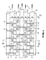
- FIG.1 The planar view of the configuration of two horizontal registers 2, 3 of the CCD 1 is shown in FIG.1, and the cross section taken along the II-II line of FIG.1 is shown in FIG. 2.
- the horizontal register 2 includes a linear first electrode II and a linear second electrode 12 each having their length direction arranged in the horizontal direction (direction H in the figure) and having line widths W.
- These first and second electrodes 11, 12 are formed by patterning a polysilicon layer of the first layer.
- the first and second electrodes 11, 12 are spaced by a distance S.
- a p-type silicon substrate 30 is constituted by a silicon oxide film 31.
- An n+ type impurity region 32 is-formed as the first region in the surface of the p-type silicon substrate 30 located below the first electrode 11. Similary in the surface of the silicon substrate 30 located bell the second electrode 12, an n+ type impurity region 33 is forced as the second region through the silicon oxide file 31.
- the silicon oxide film 31 serves as a gate oxide film.
- the n+ type impurity region 32 below the first electrode 11 is partitioned per each bit in a direction H by channel stop regions 16.
- the channel stop regions 16 each comprise a p+ type impurity region formed in the surface of the silicon substrate 30, and are formed as a plurality of elongated patterns respectively having their length direction arranged along the V-direction. These channel stop regions 16 are contiguous to the channel stop regions of the vertical registers and terminate at the portion where they reach the second electrode 12.
- the distances l0 between respective patterns of the channel stop regions 16 are equal to the pitches between the vertical registers, and are set to the same intervals l0 with respect to each bit.
- the n+ type impurity region 32 partitioned by the channel stop regions 16 in this way is caused to serve as a plurality of first storage sections arranged in the direction H.
- the n+ type impurity region 33 below the second electrode 12 is partitioned per each bit in the direction H by channel stop regions 22.
- the channel stop regions 22 are each comprised of a p+ type impurity region formed in the surface of the silicon substrate 30 in the same manner as in the case of the channel stop regions 16, and are formed as a plurality of elongated patterns respectively having the direction V as a length direction. These channel stop regions 22 have a positional relationship such that they are shifted with respect to the channel stop regions 16 by a half bit in the direction H which is the direction of transferring charges, i.e., by the distance l0/2 in the direction H.
- channel stop regions 22 are formed in the direction V as patterns starting from the side portion of the first electrode II and terminating at the side portion of the second electrode 14 of the horizontal register 3 as described later.
- the distances l0 between respective patterns of the channel stop regions 22 are also set to the same interval with respect to respective bits.
- the n+ type impurity region 33 partitioned by the channel stop regions 22 in this way is caused to serve as a plurality of second storage sections arranged in the direction H. These second and first storage sections are opposite to each other in a manner that they are shifted by the half bit in the direction H.
- the regions between the first and second electrodes 11, 12 are allowed to serve as removed portions of the channel stop regions, and function as charge transfer paths. Namely, the regions of the spacing S between the electrodes 11, 12 are such that the channel stop regions 16 and the channel stop regions 22 are extended in the direction V one after another at intervals of half bits, and first and second transfer electrodes 10, 19 are formed one after another so as to cover the regions between respective channel stop regions 16, 22 leaving no space between them.
- These first and second transfer electrodes 15, 19 are each comprised of a polysilicon layer of the second layer, and have rectangular patterns, respectively.
- the first transfer electrodes 18 are connected to the first electrode 11 through contact holes 17 formed in interlayer oxide films 39 between the polysilicon layer of the first layer and the polysilicon layer of the second layer.
- the second transfer electrodes 19 are connected to the second electrode 12 similarly through the contact holes 17 formed in the oxide films 39.
- the end portions in the direction V of the first transfer electrodes 15 overlap with the second electrode 12, and the end portions in the direction V of the second transfer electrodes 19 overlap with the first electrode 11.
- Below the first and second transfer electrodes 18, 19, an n+ type impurity region 34 is formed through the silicon oxide film 31. Accordingly, the portions below the first and second transfer electrodes 15, 19 function as the transfer sections of the charge transfer sections.
- the potential below each first transfer electrode 15 interlocks with that of the first storage section, and the potential below each second transfer electrode 19 interlocks with that of the second storage section.
- the channel stop regions in the region between the first and second electrodes 11, 12 may be formed by self-alignment after the polysilicon layer of the second layer is formed.
- the horizontal register 3 has substantially the same structure as that of the horizontal register 2. Namely, the horizontal register 3 includes linear first and second electrodes 13, 14 respectively having line widths W and having the direction H in the figure as the length direction which are formed by patterning the polysilicon layer of the first layer, and the first and second electrodes 13, 14 are also spaced by a distance having the size S. Below the first electrode 13, there exists an n+ type impurity region 35 serving as a first region formed on the side of the surface of the p-type silicon substrate 30. Similarly on the side of the surface of the silicon substrate 30 located below the second electrode 14, an n+ type impurity region 36 is formed as a second region through the silicon oxide film 31.
- the n+ type impurity region 35 below the first electrode 13 and the n+ type impurity region 36 below the second electrode 14 are partitioned per each bit in the direction H by the channel stop regions 22, 23, respectively.
- These channel stop regions 22, 23 are each comprised of a p+ type impurity region formed on the side of the surface of the silicon substrate 30, and are formed as a plurality of patterns respectively having the direction V as the length direction. Further, the pitches in the direction H of respective channel stop regions 22, 23 are set to the same interval l0 with respect to respective bits.
- the channel stop regions 22 are extended in the direction V from the side portion of the first electrode 11 of the horizontal register 2 to the side portion of the second electrode 14 of the horizontal register 3.
- the channel stop regions 23 each begin from the side portion of the first electrode 13 and become continuous to a device isolation region 24 outside the second electrode 14.
- These channel stop regions 22 have a positional relationship such that they are shifted with respect to the channel stop regions 23 by distance l 0/2 in the direction H which is the direction of transferring charges.
- the n+ type impurity regions 35, 36 are partitioned by the channel stop regions 22, 23 to form first and second storage sections, respectively. In the same manner as in the case of the horizontal register 2, these first and second storage sections are opposite to each other so that they are shifted by half bits in the direction H.
- the region between the first and second electrodes 13, 14 of the horizontal register 3 is constituted in the same manner as in the case of the horizontal register 2. Namely, the region of the spacing S between these electrode 11, 12 is such that the channel stop regions 22, 23 are extended in the direction V one after another at intervals of half bits, and the removed portions of these channel stop regions serve as charge transfer paths. In order to cover portions between respective channel stop regions 22, 23 serving as the charge transfer paths leaving no space between them, the first and second transfer electrodes 20, 21 each comprised of a polysilicon layer of the second layer of the rectangular pattern are formed one after another.
- first transfer electrodes 20 are connected to the first electrode 13 through the contact holes 17 formed in the interlayer oxide films 39, and the second transfer electrodes 21 are also connected to the second electrode 14 through the contact holes similarly formed in the interlayer oxide films 39.
- the end portions in the direction V of the first transfer electrodes 20 overlap with the second electrode 14, and the end portions in the direction V of the second transfer electrode 21 overlap with the first electrode 13.
- an n+ type impurity region 37 is formed through the silicon oxide film 31.
- the first and second transfer electrodes 20, 21 and the n ⁇ type impurity region 37 have the same functions as those of the first and second transfer electrodes 18, 19 and the n ⁇ type impurity region 34, respectively.
- the n ⁇ type impurity region 37 functions as a storage section. It is to be noted that the channel stop regions between the first and second electrodes 13, 14 may be similarly formed by self-alignment process after the polysilicon layer of the second layer is formed.
- a transfer gate 15 serving as a transfer electrode between transfer sections is formed in the region of a width In between the charge transfer sections of the horizontal registers 2, 3.
- This transfer gate 15 is composed of a polysilicon layer of the second layer, and is formed with its length direction arranged along the direction H. The end portion in the direction V of this transfer gate 15 overlaps with the second electrode 12 of the horizontal register 2 and the first electrode 13 of the horizontal register 3 through the oxide films 39 serving as the interlayer insulating layer.
- a plurality of channel stop regions 22 are formed at intervals of l0 in the direction H, and these channel stop regions 22 are formed so as to traverse the width In, respectively.
- the region between which a pair of channel stop regions 22 are put is a channel region 38 comprised of an n ⁇ type impurity region, and serves as a charge transfer path when transfer between horizontal registers is carried out.
- a channel region 38 comprised of an n ⁇ type impurity region, and serves as a charge transfer path when transfer between horizontal registers is carried out.
- one first storage section of the horizontal register 2 is caused to correspond to one first storage section of the horizontal register 3 through the channel region 38 below the transfer gate 15.
- the horizontal registers 2, 3 of the abovementioned structure can carry out a charge transfer in the direction H and carry out a transfer in the direction V, i .e., a charge transfer from the horizontal register 2 to the horizontal register 3.
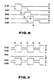
- a signal H1 ⁇ 1 delivered to the first electrode 11 of the horizontal register 2 is first caused to be at high (H) level, so that a signal t is produced and transfer from the vertical register 5 into the first region of the horizontal register 2 is carried out.
- signal charge generated by photoelectric conversion at the light receiving sections 4 are passed from the vertical registers 5 through the portions between respective channel stop regions 16, and are then stored into the n+ type impurity region 32 below the first electrode 11 of the horizontal register 2.
- This n+ type impurity region 32 is partitioned by the channel stop regions 16 per each bit, and respective sections are electrically connected through contact holes 17.
- the n ⁇ type impurity region 34 below the first transfer electrode 18 to which a signal H1 ⁇ 1 is given is caused to serve as a transfer section. Since a signal H1 ⁇ 2 delivered to the second transfer electrode 19 and the second electrode 12 is at low (L) level at the time t1, signal charges are stored only into the portion below the first electrode 11.
- the signal H1 ⁇ 1 charges to L level and the signal H1 ⁇ 2 changes from L level to H level.
- the potential well below the first electrode 11 and the first transfer electrode 18 becomes shallow, and the potential well below the second electrode 12 and the second transfer electrode 19 becomes deep.
- signal charge stored in the n-type impurity region 32 are stored into the n+ type impurity region 33 below the second electrode 12 through the portion below the second transfer electrode 19.
- the potential well below the first transfer electrode 15 is at all time shallower than that below the first electrode 11, sweeping away of signal charges to adjacent bits is avoided, so transfer of charges in a direction indicated by broken lines in FIG. 4 is necessarily carried out.
- a signal ⁇ TG delivered to the transfer gate 15 changes from L level to H level at time t3.
- the channel region 38 below the transfer gate 15 becomes conductive by this signal ⁇ TG. so signal charges are transferred into the portion below the transfer gate 15.
- the signal H2 ⁇ 1 delivered to the first electrode 13 of the horizontal register 3 changes from L level to H level.
- the signal H1 ⁇ 2 delivered to the second electrode 12 of the horizontal register 2 changes from H level to L level.
- charges stored in the n+ type impurity region 33 below the second electrode 12 of the horizontal register 2 are transferred into the n+ type impurity region 35 below the first electrode 13 of the horizontal register 3 through the channel region 38 below the transfer gate 15 placed in a conductive state.
- the signal ⁇ TG delivered to the transfer gate 15 changes to L level, so the channel region 38 is in a cutoff state. At this time, signal charges are stored into the n+ type impurity region 35 below the first electrode 13 of the horizontal register 3.
- the signal H2 ⁇ 1 delivered to the first electrode 13 of the horizontal register 3 shifts from H level to L level for a second time.
- the signal H2 ⁇ 2 delivered to the second electrode 14 of the same horizontal register 3 shifts in turn from L level to H level.
- clock signals are delivered to the first electrodes 11, 13 and the second electrodes 12 and 14, respectively.
- the signal H1 ⁇ 1 delivered to the first electrode 11 and the signal H1 ⁇ 2 delivered to the second electrode 12 of the horizontal register 2 are complementary clock signals.
- the signal H2 ⁇ 1 delivered to the first electrode 13 and the signal H2 ⁇ 2 delivered to the second electrode 12 of the horizontal register 3 are also complementary clock signals. These clock signals all have the same frequency.
- the signals H1 ⁇ 1 and H2 ⁇ 2 are placed at H level and the signals H1 ⁇ 2 and H2 ⁇ 2 are placed at L level.
- the horizontal registers 2, 3 charges are transferred into the n+ type impurity region 32, 35 caused to serve as the first storage section below the first electrodes 11, 13 through the n ⁇ type impurity regions 34, 37 below the first transfer electrodes 18, 20, respectively.
- the signals H1 ⁇ 1 and H2 ⁇ 1 are placed at L level and the signals H1 ⁇ 2 and H2 ⁇ 2 are placed at H level.
- signal charges stored in the first storage section below the first electrodes 11, 13 are transferred into the n+ type impurity regions 33, 36 caused to serve as the second storage section below the second electrodes 12, 14 through the n ⁇ type impurity regions 34, 37 below the second transfer electrodes 19, 21.
- the operations at the times t a and t b are repeatedly performed.
- signal charges are transferred interchangeably through the first and second storage sections by half bit at respective clocks. Thus, they are transferred in the direction H.
- the CCD 1 where both the transfer in the horizontal direction and the transfer in the vertical direction are carried out as stated above is such that transfer between horizontal registers in the vertical direction is implemented to the first storage section through the channel region 38 below the transfer gate 15 from the second storage section having a width l0 corresponding to one bit partitioned by narrow channel stop regions 22.
- the width l0 of transfer between horizontal registers is set to a width twice larger than that of the conventional two-phase system which is not in the form of meander.
- the channel region 35 can be a broad area. In addition, this is convenient in processing, and is also advantageous in implementation of miniaturization.
Landscapes
- Solid State Image Pick-Up Elements (AREA)
Applications Claiming Priority (2)
| Application Number | Priority Date | Filing Date | Title |
|---|---|---|---|
| JP250530/89 | 1989-09-28 | ||
| JP1250530A JPH03114236A (ja) | 1989-09-28 | 1989-09-28 | 電荷転送装置 |
Publications (3)
| Publication Number | Publication Date |
|---|---|
| EP0420764A2 true EP0420764A2 (de) | 1991-04-03 |
| EP0420764A3 EP0420764A3 (en) | 1991-07-24 |
| EP0420764B1 EP0420764B1 (de) | 1997-03-19 |
Family
ID=17209268
Family Applications (1)
| Application Number | Title | Priority Date | Filing Date |
|---|---|---|---|
| EP90402694A Expired - Lifetime EP0420764B1 (de) | 1989-09-28 | 1990-09-28 | Ladungsverschiebeanordnung mit mäanderförmigem Kanal |
Country Status (4)
| Country | Link |
|---|---|
| US (1) | US5075747A (de) |
| EP (1) | EP0420764B1 (de) |
| JP (1) | JPH03114236A (de) |
| DE (1) | DE69030227T2 (de) |
Cited By (2)
| Publication number | Priority date | Publication date | Assignee | Title |
|---|---|---|---|---|
| WO1997020351A1 (en) * | 1995-11-29 | 1997-06-05 | Massachusetts Institute Of Technology | Multidirectional transfer charge-coupled device |
| US7646042B2 (en) * | 2005-01-24 | 2010-01-12 | Sanyo Electric Co., Ltd. | Charge coupled device and solid-state imaging apparatus |
Families Citing this family (3)
| Publication number | Priority date | Publication date | Assignee | Title |
|---|---|---|---|---|
| KR960001182B1 (ko) * | 1992-05-20 | 1996-01-19 | 삼성전자주식회사 | 고체 촬상 소자 |
| KR100239409B1 (ko) * | 1997-01-25 | 2000-01-15 | 김영환 | 고체 촬상 소자 |
| US7602431B2 (en) * | 2005-09-28 | 2009-10-13 | Sony Corporation | Solid-state imaging element and solid-state imaging apparatus |
Family Cites Families (11)
| Publication number | Priority date | Publication date | Assignee | Title |
|---|---|---|---|---|
| DE2646301C3 (de) * | 1975-10-31 | 1981-01-15 | Fujitsu Ltd., Kawasaki, Kanagawa (Japan) | Ladungsgekoppeltes Halbleiterbauelement |
| JPS5814749B2 (ja) * | 1976-04-15 | 1983-03-22 | 富士通株式会社 | 電荷転送装置 |
| US4103347A (en) * | 1976-10-29 | 1978-07-25 | Texas Instruments Incorporated | Zig-zag sps ccd memory |
| DE2842856C3 (de) * | 1978-10-02 | 1981-09-03 | Siemens AG, 1000 Berlin und 8000 München | Ladungsverschiebespeicher in Seriell-Parallel-Seriell-Organisation mit vollständigem Grundladungsbetrieb |
| US4291239A (en) * | 1980-02-25 | 1981-09-22 | Rca Corporation | Architecture line-transfer CCD imagers |
| US4380056A (en) * | 1980-10-10 | 1983-04-12 | Hughes Aircraft Company | Charge coupled device focal plane with serial register having interdigitated electrodes |
| US4446473A (en) * | 1981-04-30 | 1984-05-01 | Fairchild Camera & Instrument Corporation | Serpentine charge transfer device |
| JPS6041374A (ja) * | 1983-08-16 | 1985-03-05 | Canon Inc | 撮像装置 |
| JPS6169173A (ja) * | 1984-09-12 | 1986-04-09 | Sanyo Electric Co Ltd | 電荷結合素子 |
| NL8800627A (nl) * | 1988-03-15 | 1989-10-02 | Philips Nv | Ladingsgekoppelde inrichting. |
| US4987466A (en) * | 1988-06-07 | 1991-01-22 | Kabushiki Kaisha Toshiba | Solid state image sensor |
-
1989
- 1989-09-28 JP JP1250530A patent/JPH03114236A/ja active Pending
-
1990
- 1990-09-28 US US07/589,690 patent/US5075747A/en not_active Expired - Fee Related
- 1990-09-28 EP EP90402694A patent/EP0420764B1/de not_active Expired - Lifetime
- 1990-09-28 DE DE69030227T patent/DE69030227T2/de not_active Expired - Fee Related
Cited By (3)
| Publication number | Priority date | Publication date | Assignee | Title |
|---|---|---|---|---|
| WO1997020351A1 (en) * | 1995-11-29 | 1997-06-05 | Massachusetts Institute Of Technology | Multidirectional transfer charge-coupled device |
| US5760431A (en) * | 1995-11-29 | 1998-06-02 | Massachusetts Institute Of Technology | Multidirectional transfer charge-coupled device |
| US7646042B2 (en) * | 2005-01-24 | 2010-01-12 | Sanyo Electric Co., Ltd. | Charge coupled device and solid-state imaging apparatus |
Also Published As
| Publication number | Publication date |
|---|---|
| EP0420764B1 (de) | 1997-03-19 |
| DE69030227T2 (de) | 1997-07-10 |
| JPH03114236A (ja) | 1991-05-15 |
| US5075747A (en) | 1991-12-24 |
| EP0420764A3 (en) | 1991-07-24 |
| DE69030227D1 (de) | 1997-04-24 |
Similar Documents
| Publication | Publication Date | Title |
|---|---|---|
| US5510285A (en) | Method for fabricating CCD image sensors | |
| US5289022A (en) | CCD shift register having a plurality of storage regions and transfer regions therein | |
| US6707495B1 (en) | Solid-state imaging device and a method of reading a signal charge in a solid-state imaging device which can reduce smear and can provide an excellent image characteristic | |
| US5040038A (en) | Solid-state image sensor | |
| US6114717A (en) | Solid-state imaging device having no transfer error of the signal charges from vertical horizontal charge-transfer section | |
| EP0444696B1 (de) | Festkörperbildabtaster | |
| JPS5983477A (ja) | 撮像方式 | |
| EP0420764B1 (de) | Ladungsverschiebeanordnung mit mäanderförmigem Kanal | |
| US5182622A (en) | Charge coupled device imager having multichannel readout structure | |
| US4649407A (en) | Charge coupled device for transferring electric charge | |
| US5502319A (en) | Solid state image sensor with non-parallel conductors | |
| EP0383519B1 (de) | Ladungsgekoppelte Abbildungsanordnung mit Mehrkanallesestruktur | |
| US5060038A (en) | Charge sweep solid-state image sensor | |
| JP3072505B2 (ja) | Ccd | |
| JP2877047B2 (ja) | 固体撮像装置 | |
| US7595517B2 (en) | Charge coupled device having diverged channel | |
| KR0165338B1 (ko) | Ccd형 고체촬영소자, 이를 제조하는 방법 및 이를 구동하는 방법 | |
| JP3002365B2 (ja) | 電荷転送装置及びその駆動方法 | |
| JP3028823B2 (ja) | 電荷結合素子およびこれを用いた固体撮像装置 | |
| JP3180742B2 (ja) | Ccd型固体撮像装置及びその製造方法 | |
| KR100271804B1 (ko) | 고체촬상소자 및 그 구동방법 | |
| JPH0513746A (ja) | 固体撮像装置 | |
| JP2853779B2 (ja) | 固体撮像装置 | |
| JP2892547B2 (ja) | 電荷結合素子 | |
| JPH1022492A (ja) | 固体撮像素子の製造方法 |
Legal Events
| Date | Code | Title | Description |
|---|---|---|---|
| PUAI | Public reference made under article 153(3) epc to a published international application that has entered the european phase |
Free format text: ORIGINAL CODE: 0009012 |
|
| AK | Designated contracting states |
Kind code of ref document: A2 Designated state(s): DE FR GB |
|
| PUAL | Search report despatched |
Free format text: ORIGINAL CODE: 0009013 |
|
| AK | Designated contracting states |
Kind code of ref document: A3 Designated state(s): DE FR GB |
|
| 17P | Request for examination filed |
Effective date: 19920109 |
|
| 17Q | First examination report despatched |
Effective date: 19940822 |
|
| GRAG | Despatch of communication of intention to grant |
Free format text: ORIGINAL CODE: EPIDOS AGRA |
|
| GRAH | Despatch of communication of intention to grant a patent |
Free format text: ORIGINAL CODE: EPIDOS IGRA |
|
| GRAH | Despatch of communication of intention to grant a patent |
Free format text: ORIGINAL CODE: EPIDOS IGRA |
|
| GRAA | (expected) grant |
Free format text: ORIGINAL CODE: 0009210 |
|
| AK | Designated contracting states |
Kind code of ref document: B1 Designated state(s): DE FR GB |
|
| REF | Corresponds to: |
Ref document number: 69030227 Country of ref document: DE Date of ref document: 19970424 |
|
| ET | Fr: translation filed | ||
| PLBE | No opposition filed within time limit |
Free format text: ORIGINAL CODE: 0009261 |
|
| STAA | Information on the status of an ep patent application or granted ep patent |
Free format text: STATUS: NO OPPOSITION FILED WITHIN TIME LIMIT |
|
| 26N | No opposition filed | ||
| PGFP | Annual fee paid to national office [announced via postgrant information from national office to epo] |
Ref country code: FR Payment date: 20010911 Year of fee payment: 12 |
|
| PGFP | Annual fee paid to national office [announced via postgrant information from national office to epo] |
Ref country code: GB Payment date: 20010926 Year of fee payment: 12 |
|
| PGFP | Annual fee paid to national office [announced via postgrant information from national office to epo] |
Ref country code: DE Payment date: 20011015 Year of fee payment: 12 |
|
| REG | Reference to a national code |
Ref country code: GB Ref legal event code: IF02 |
|
| PG25 | Lapsed in a contracting state [announced via postgrant information from national office to epo] |
Ref country code: GB Free format text: LAPSE BECAUSE OF NON-PAYMENT OF DUE FEES Effective date: 20020928 |
|
| PG25 | Lapsed in a contracting state [announced via postgrant information from national office to epo] |
Ref country code: DE Free format text: LAPSE BECAUSE OF NON-PAYMENT OF DUE FEES Effective date: 20030401 |
|
| GBPC | Gb: european patent ceased through non-payment of renewal fee |
Effective date: 20020928 |
|
| PG25 | Lapsed in a contracting state [announced via postgrant information from national office to epo] |
Ref country code: FR Free format text: LAPSE BECAUSE OF NON-PAYMENT OF DUE FEES Effective date: 20030603 |
|
| REG | Reference to a national code |
Ref country code: FR Ref legal event code: ST |