EP0420974B1 - Amplificateur a circuits accordes - Google Patents
Amplificateur a circuits accordes Download PDFInfo
- Publication number
- EP0420974B1 EP0420974B1 EP90907518A EP90907518A EP0420974B1 EP 0420974 B1 EP0420974 B1 EP 0420974B1 EP 90907518 A EP90907518 A EP 90907518A EP 90907518 A EP90907518 A EP 90907518A EP 0420974 B1 EP0420974 B1 EP 0420974B1
- Authority
- EP
- European Patent Office
- Prior art keywords
- input
- output
- resonance amplifier
- transconductance
- loop
- Prior art date
- Legal status (The legal status is an assumption and is not a legal conclusion. Google has not performed a legal analysis and makes no representation as to the accuracy of the status listed.)
- Expired - Lifetime
Links
- 230000015572 biosynthetic process Effects 0.000 claims abstract description 11
- 238000003786 synthesis reaction Methods 0.000 claims abstract description 11
- 230000001172 regenerating effect Effects 0.000 claims abstract description 8
- 238000001514 detection method Methods 0.000 claims description 2
- 230000003321 amplification Effects 0.000 abstract description 11
- 238000003199 nucleic acid amplification method Methods 0.000 abstract description 11
- 230000007423 decrease Effects 0.000 abstract description 9
- 230000009467 reduction Effects 0.000 abstract description 3
- 230000001419 dependent effect Effects 0.000 description 13
- 230000001965 increasing effect Effects 0.000 description 7
- 230000010363 phase shift Effects 0.000 description 7
- 239000003990 capacitor Substances 0.000 description 6
- 230000003044 adaptive effect Effects 0.000 description 5
- 238000006243 chemical reaction Methods 0.000 description 4
- 230000003247 decreasing effect Effects 0.000 description 4
- 230000000694 effects Effects 0.000 description 4
- 230000010355 oscillation Effects 0.000 description 4
- 230000003071 parasitic effect Effects 0.000 description 4
- 230000001550 time effect Effects 0.000 description 4
- 238000010586 diagram Methods 0.000 description 3
- 230000006641 stabilisation Effects 0.000 description 3
- 238000011105 stabilization Methods 0.000 description 3
- 230000009471 action Effects 0.000 description 2
- 230000005540 biological transmission Effects 0.000 description 2
- 230000007850 degeneration Effects 0.000 description 2
- 238000005516 engineering process Methods 0.000 description 2
- 238000001914 filtration Methods 0.000 description 2
- 230000010354 integration Effects 0.000 description 2
- 230000005855 radiation Effects 0.000 description 2
- 230000005236 sound signal Effects 0.000 description 2
- 230000006978 adaptation Effects 0.000 description 1
- 230000008878 coupling Effects 0.000 description 1
- 238000010168 coupling process Methods 0.000 description 1
- 238000005859 coupling reaction Methods 0.000 description 1
- 238000006880 cross-coupling reaction Methods 0.000 description 1
- 230000006872 improvement Effects 0.000 description 1
- 230000001939 inductive effect Effects 0.000 description 1
- 238000009413 insulation Methods 0.000 description 1
- 239000000758 substrate Substances 0.000 description 1
- 230000001629 suppression Effects 0.000 description 1
Images




Classifications
-
- H—ELECTRICITY
- H03—ELECTRONIC CIRCUITRY
- H03H—IMPEDANCE NETWORKS, e.g. RESONANT CIRCUITS; RESONATORS
- H03H11/00—Networks using active elements
- H03H11/02—Multiple-port networks
- H03H11/04—Frequency selective two-port networks
-
- H—ELECTRICITY
- H03—ELECTRONIC CIRCUITRY
- H03H—IMPEDANCE NETWORKS, e.g. RESONANT CIRCUITS; RESONATORS
- H03H11/00—Networks using active elements
- H03H11/02—Multiple-port networks
- H03H11/04—Frequency selective two-port networks
- H03H11/0422—Frequency selective two-port networks using transconductance amplifiers, e.g. gmC filters
- H03H11/0472—Current or voltage controlled filters
-
- H—ELECTRICITY
- H03—ELECTRONIC CIRCUITRY
- H03F—AMPLIFIERS
- H03F3/00—Amplifiers with only discharge tubes or only semiconductor devices as amplifying elements
- H03F3/189—High-frequency amplifiers, e.g. radio frequency amplifiers
- H03F3/19—High-frequency amplifiers, e.g. radio frequency amplifiers with semiconductor devices only
- H03F3/191—Tuned amplifiers
-
- H—ELECTRICITY
- H03—ELECTRONIC CIRCUITRY
- H03H—IMPEDANCE NETWORKS, e.g. RESONANT CIRCUITS; RESONATORS
- H03H11/00—Networks using active elements
- H03H11/02—Multiple-port networks
- H03H11/04—Frequency selective two-port networks
- H03H11/0422—Frequency selective two-port networks using transconductance amplifiers, e.g. gmC filters
- H03H11/0433—Two integrator loop filters
Definitions
- the invention also relates to a frequency synthesis circuit comprising a frequency divider circuit, a phase detector, a loop filter and a voltage-controlled oscillator successively incorporated in a phase-locked loop.
- a tunable resonance amplifier of this type is known, for example, from German Patent Specification no. 1,262,466.
- a frequency synthesis circuit of this type is known, for example, by the type indication LM 7005 of Sanyo.
- the known resonance amplifier successively comprises a voltage signal adding circuit, an inverting cnjontrollable voltage amplifier and an RC network composed of a cascade arrangement of the first and the second first-order low-pass RC filters.
- the output of the resonance amplifier is connected to the adder circuit via the feedback path, resulting in a DC negative feedback loop with a controlled loop gain.
- the known resonance amplifier has a selective gain which increases with an increasing tuning frequency, and conversely.
- the increase of the selective gain can be reduced with an increasing tuning frequency by means of an extra integrator arranged in series with the signal path, such an integrator introduces unwanted effects such as, for example a very strong increase of the output signal of the amplifier at a tuning frequency decreasing to zero.
- the field of use of this known tunable resonance amplifier is comparatively small, also because of this frequency-dependent selective gain. Application in, for example, receiver tuning devices for a tunable channel RF selection of a desired RF reception signal is not possible.
- the tunable resonance amplifier according to the invention is therefore suitable for many applications, inter alia for realising in radio and TV receivers a tunable channel RF selection and/or for realising a fixed IF selection of a desired RF or IF reception signal in the case of a suitably chosen tuning.
- a tunable resonance amplifier according to the invention is preferably characterized in that the loop comprises in a closed loop form and successively arranged in cascade a first controlled amplifier, the first RC filter, a second controlled amplifier and the second RC filter, the two amplifiers and the two RC filters being mutually substantially identical.
- each of the two amplifiers can be varied in gain over a comparatively large control range without unwanted phenomena such as, for example saturation occurring therein.
- the tuning range of the resonance amplifier according to the invention is increased considerably.
- this preferred embodiment is not only suitable for a frequency selection of single-phase signals but, with suitably chosen input and output terminals, it is also suitable for selecting phase quadrature signals or it is suitable as a selective phase splitter or as a selective adder circuit.
- the third and fourth transconductance circuits constitute an extra resistor parallel to the load resistor and the capacitive load and a reduction of the power dissipation and a decrease of the required power supply voltage is obtained.
- a further embodiment of such a resonance amplifier which is characterized in that the transconductances of the third and fourth transconductance circuits are controllable, provides the possibility of reducing the bandwidth by varying the last-mentioned transconductances and of simultaneously increasing the gain, or conversely.
- each one of the third and fourth transconductance circuits is positively fed back from the output to the input.
- the third and fourth transconductance circuits constitute a negative resistor, therewith enabling a high effective load resistor to be realised when using a comparatively small load resistor without an increase of the power supply voltage and hence the power dissipation.
- An embodiment in which the gain of the tunable resonance amplifier can be adjusted in a simple manner is characterized in that the input signal of the resonance amplifier is applied via an input transconductance circuit to the input of at least one of the two first and second transconductance circuits.
- a further embodiment is characterized in that the input transconductance circuit is controllable.
- a practical embodiment which is particularly suitable for integration is characterized in that the first and second transconductance circuits comprise first and second difference pairs, respectively, which first and second difference pairs comprise first and second, and third and fourth emitter-coupled transistors with a first and a second current source transistor arranged in a common emitter tail configuration, said two current source transistors being controllable from a first common control circuit having a tuning control input for controlling the transconductance of the first and second transconductance circuits, the collectors of said first to fourth transistors each being connected to the power supply voltage via first to fourth load resistors, respectively, and being coupled to the bases of the fourth, third, first and second transistors, while first and second capacitances are arranged between the collectors of the first and second, and the third and fourth transistors, respectively.
- the load resistors are not only used for a desired attenuation of the selective operation of the loop circuit but they also simplify the realisation of a suitable working point of the transistors.
- first and second load series resistors are arranged in series with the first and second capacitances respectively. Said load series resistors reduce the phase shift effect due to parasitic delay times in the difference pairs.
- a preferred embodiment using a little critical and hence accurate control of the transconductance of the third and fourth transconductance circuits is characterized in that an emitter resistor is incorporated in the emitter lead of each one of the fifth to eighth transistors.
- An embodiment which is particularly suitable for very high frequencies, for example in the TV satellite frequency range is characterized in that the fifth to eighth transistors are fed back from collector to base via the base-emitter junction of ninth to twelfth transistors, respectively, and in that the collectors of the first to fourth transistors are coupled to the bases of the fourth, third, first and second transistors, respectively.
- the cut-off frequency of the signal-processing transistors is increased.
- a practical embodiment of the input transconductance circuit is characterized in that the input transconductance circuit comprises a differential stage having first and second emitter-coupled input transistors and a current source in a common emitter lead whose collectors are connected to the bases of the transistors of one of the two difference pairs.
- the known frequency synthesis circuit utilizes a wideband amplifier between the voltage-controlled tuning oscillator and the frequency divider in order to comply with the existing radiation requirements and it has a comparatively complex and hence expensive circuit configuration.
- the invention has for its second object to provide a frequency synthesis circuit which can be realised, inter alia at lower cost and has less power dissipation than the known frequency synthesis circuit.
- such a frequency synthesis circuit is therefore characterized in that a tunable resonance amplifier as described hereinbefore is arranged between the voltage-controlled oscillator and the frequency divider circuit, the loop filter being coupled to a tuning control input of the tunable resonance amplifier for simultaneously tuning the voltage-controlled oscillator and the tunable resonance amplifer.
- a comparatively high selective amplification of the oscillator signal can be obtained by means of the tunable resonance amplifier with only a comparatively small power dissipation, so that the oscillator signal amplitude may be chosen to be small.
- Such a superheterodyne AM receiver successively comprising an RF input section, a tunable mixer stage, an AM-IF section and an AM demodulation device is characterized in that the AM-IF section comprises a tunable resonance amplifier comprising a non regenerative DC negative feedback loop which includes controlled amplifying means providing a controlled loop gain, said loop incorporating first and second first-order low-pass RC filters, and having a signal path arranged from the input to the output and a feedback path arranged from the output to the input, the signal path incorporating one of the two said filters and the feedback path incorporates the other filter together with the controlled amplifying means, or the controlled amplifying means comprising two controlled amplifiers and the signal path incorporating the two said filters together with one of said amplifiers and the feedback path incorporating the other of said amplifiers, said controlled amplifying means being realised by first and second transconductance circuits each having a controllable transconductance from a voltage input to a current output, and in that in the loop the current outputs of
- a superheterodyne FM receiver successively comprising an RF input section, a tunable mixer stage, an FM-IF section and an FM demodulation device is characterized in that the FM-IF section comprises a tunable resonance amplifier comprising a non regenerative DC negative feedback loop which includes controlled amplifying means providing a controlled loop gain, said loop incorporating first and second first-order low-pass RC filters, and having a signal path arranged from the input to the output and a feedback path arranged from the output to the input, the signal path incorporating one of the two said filters and the feedback path incorporates the other filter together with the controlled amplifying means, or the controlled amplifying means comprising two controlled amplifiers and the signal path incorporating the two said filters together with one of said amplifiers and the feedback path incorporating the other of said amplifiers, said controlled amplifying means being realised by first and second transconductance circuits each having a controllable transconductance from a voltage input to a current output, and in that in the loop the current outputs of the first
- Fig. 1 shows the basic circuit diagram of the known tunable resonance amplifier according to said German Patent Specification no. 1,262,466, which selectively amplifies an input signal voltage V in applied to an input IN to an output signal voltage V out at an output OUT.
- the known resonance amplifier comprises a non-regenerative loop having a signal path from the input IN to the output OUT successively incorporating: a voltage adder circuit S, a controlled voltage amplifier VA and a cascade circuit of first and second first-order RC low-pass filters R1C1 and R2C2, respectively.
- Each low-pass filter R1C1 and R2C2 comprises a serial resistor R1, R2 and a parallel capacitor C1, C2, respectively, connected to ground.
- Figs. 2a and 2b are block diagrams of first and second embodiments of a tunable resonance amplifier according to the invention, each amplifier selectively amplifying an input signal voltage V in applied to the input IN to an output signal voltage V out at the output OUT.
- the controlled loop gain in said second embodiment is not realised by means of a single controllable voltage amplifier but by the cascade circuit of several controllable voltage amplifiers each realising a part and jointly realising the total loop gain.
- the version shown in Fig. 2b comprises a cascade circuit of first and second controllable voltage amplifiers denoted by VA1 and VA2, respectively.
- the voltage amplifiers VA1 and VA2 preferably have a mutually equal amplification so that each of them realises half the total loop gain in dB and a signal inversion takes place in one of these voltage amplifiers.
- Fig. 2c shows a third embodiment of a tunable resonance amplifier according to the invention which can be more easily realised in practice as compared with that shown in Figs. 2a and 2b.
- the loop is formed by a cascade circuit of first and second transconductance circuits TC1 and TC2 having a controllable transconductance whose outputs are coupled to a parallel circuit, functioning as the first low-pass filter R1C1, of a first load capacitor C1 and a first load resistor R1 and a parallel circuit, functioning as the second low-pass filter R2C2, of a second load capacitor C2 and a second load resistor R2, respectively, said two parallel circuits being connected to ground.
- the two transconductance circuits TC1 and TC2 together with the parallel circuits R1C1 and R2C2 constitute first and second sections which mutually correspond.
- the output of the second transconductance circuit TC2 is connected to the input of the first transconductance circuit TC1 via a voltage inverter circuit INV.
- the resonance frequency is the frequency for which the gain of one occurs in the closed loop.
- the phase shift at the resonance frequency across each section appears to be 90° in a very close approximation, but with a suitable dimensioning there is a sufficient phase margin left to avoid oscillation.
- the loop circuit has a bandpass characteristic whose resonance frequency is controllable by means of a variation of the transconductance of TC1 and TC2 and whose bandwidth is adjustable by means of a correctly chosen RC value for the parallel circuits R1C1 and R2C2.
- the inverter INV can be incorporated at any arbitrary position in the loop and may be omitted if a signal inversion takes place in one of the transconductances TC1 and TC2.
- the section formed by TC1 and R1C1 is preferably equal to the section formed by TC2 and R2C2.
- a signal inversion is simply obtained by providing a cross-coupling in the loop, which will be further described with reference to Figs. 5 and 7.
- the transconductance circuits TC1 and TC2 each supply output currents I o1 and I o2 , respectively, which vary with input voltages V i1 , and V i2 , the transconductances I o1 /V i1 and I o2 /V i2 being controllable.
- the controllable voltage-current conversion in TC1 and TC2 thus obtained is succeeded by a fixed current-voltage conversion across R1C1 and R2C2, respectively, so that together with the voltage inverter INV a DC negative feedback is obtained in the loop and a loop gain is obtained which is controllable by controlling the transconductances of TC1 and TC2.
- the tunable resonance amplifier is used for filtering a pair of phase quadrature signals, the first and second terminals (I/0)1 and (I/0)2 constituting both a phase quadrature current input terminal pair and a phase quadrature voltage output terminal pair.
- an input signal current I in is applied, for example to the first terminal (I/0)1 and is added at the junction point S1 to the output current I o1 of TC1.
- the output impedance of TC1, viewed from S1 is inductive and may be considered to be replaced by a coil L1 (not shown) which is arranged parallel across R1C1.
- the voltage at S1 across R1C1 is thereby mainly in phase with the input signal current I in at the resonance frequency f res of the resonance amplifier and is equal to the sum of the sub-voltages which are produced by each of the currents I in and I o1 across R1C1. This voltage is available at the first terminal (I/0)1 as output signal voltage V out .
- the signal path of the loop from the current input to the voltage output incorporates the first low-pass filter R1C1 in this first mode and the feedback path of the loop from the voltage output to the current input incorporates the cascade circuit of TC2, R2C2, INV and TC1.
- TC1 and TC2 realise the controlled loop gain.
- an input signal current I′ in at the second terminal (I/0)2 results in an output voltage V out at S2 across R2C2 which is substantially in phase with the input signal current I′ in at f ref and which is the sum of the sub-voltages produced by I′ in and the output current of TC2, I o2 across R 2C2 .
- the signal path of the loop from the current input to the voltage output incorporates the second low-pass filter R2C2 and the feedback path of the loop from the voltage output to the current input incorporates the cascade circuit of INV TC1, R1C1 and TC2.
- (I/0)1 and (I/0)2 constitute in-phase and quadrature terminals, respectively, to which the in-phase and quadrature components of a phase quadrature input signal current are applied.
- the in-phase and quadrature components of the phase quadrature output signal voltage produced by this phase quadrature input signal current become available at the same terminals (I/0)1 and (I/0)2 respectively.
- the signal path of the loop from the current input to the voltage output incorporates the cascade circuit of the first low-pass filter R1C1 the second transconductance TC2 and the second low-pass filter R2C2 and the feedback path from the voltage output to the current input incorporates the inverter circuit INV as well as the first transconductance TC1. Consequently the controlled loop gain is evenly distributed over the signal and feedback paths of the loop in the case of a symmetrical implementation in this second mode.
- an input current I in applied to (1/0)1 produces a voltage at S1 which is substantially in phase with I in .
- Fig. 3 shows a preferred embodiment of a tunable resonance amplifier RA according to the invention, based on the amplifier shown in Fig. 2c.
- the preferred embodiment shown has an input with in-phase and quadrature voltage input terminals Vi and Vq and an output with in-phase and quadrature voltage output terminals VI and VQ.
- VI and VQ correspond to the first and second terminals (I/0)1 and (I/0)2, respectively, of Fig. 2c.
- the tunable resonance amplifier RA comprises third and fourth transconductance circuits TC3 and TC4 each of which is fed back from output to input and is arranged at the outputs of TC1 and TC2, respectively.
- These transconductance circuits TC3 and TC4 realise an extra resistor which can be considered to be arranged parallel to the parallel circuits R1C1 and R2C2, respectively.
- R1 and R2 can be chosen to be small by using this measure so that, dependent on the form of realisation, the power supply voltage and hence the power dissipation can be maintained at a low value.
- a negative feedback (not shown) from output to input, for example by means of an inverter circuit in the signal path of TC3 and TC4 (not shown) they realise a positive resistor with which an attenuation of the bandpass characteristic of the resonance amplifier is possible and with which phase shifts due to parasitic delay time effects can be compensated.
- a positive or negative feedback of TC3 and TC4 is used in order to obtain a correct operation of the resonance amplifier.
- the transconductance of TC3 and TC4 can be adjusted at a fixed value.
- the tunable resonance amplifier RA shown has an input transconductance circuit comprising first and second input transconductance divider circuits TC5 and TC6.
- the circuits TC5 and TC6 are arranged between the in-phase input terminal Vi and the junction point S1 and between the quadrature input terminal Vq and the junction point S2.
- the output of TC1, or 51, and the output of TC2, or 52, are coupled to the in-phase output terminal VI and the quadrature output terminal VQ respectively, of the tunable resonance amplifier RA.
- the input transconductance circuit TC5, TC6 converts a pair of phase quadrature input voltages into a pair of phase quadrature input currents and applies these currents to the loop circuits at said junction points between which one of the two first and second transconductance circuits TC1 and TC2 is arranged.
- the phase quadrature relation of the phase quadrature input voltages to be amplified is maintained.
- the amplified phase quadrature voltages are coupled out from said points in the loop circuit.
- a variation of TC3 and TC4 results in a variation of said gain factor, which can be compensated for over a large tuning range by a suitable control of TC5 and TC6.
- Figs. 4a to 4f show a number of connection and coupling-out possibilities of the tunable resonance amplifier RA according to the invention in which the elements corresponding to those of Fig. 3 have the same references.
- Fig. 4b also shows a common supply of a single input signal voltage to Vi and Vq, the tunable resonance amplifier RA functioning as a selective phase splitter.
- a single input voltage is selectively amplified and converted or split up into a pair of phase quadrature output voltages.
- Fig. 4c shows the supply of a single input voltage to Vi and the decrease of a single output voltage at VQ which is shifted 90° or substantially 90° in phase with respect to Vi.
- Fig. 4d shows the supply of a single input voltage to Vi and an addition of the phase quadrature output voltages obtained from this input voltage and resulting in a single output voltage.
- Fig. 4f shows the tunable resonance amplifier RA as a selective interface stage from quadrature to non-quadrature signals in which a pair of phase quadrature input voltages is selectively amplified in a pair of phase quadrature output voltages, which output voltages are mutually added in an adder circuit and result in a single output voltage.
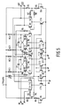
- Fig. 5 shows a practical embodiment of a tunable resonance amplifier according to the invention which is particularly suitable to be realised in bipolar IC technology with first to fourth controllable transconductance circuits comprising first to eighth transistors T1 to T8 and first to fourth current source transistors CT1 to CT4 each of which functions as a controllable current source.
- the emitters of T1 and T2, and T3 and T4 are mutually directly coupled and those of T5 and T6, and T7 and T8 are each connected to a common emitter tail via a degeneration resistor Re.
- the emitter tail of the first to fourth difference pairs T1 T2; T3, T4; T5, T6 and T7, T8 thus obtained incorporates the current source transistors CT1 to CT4.
- the current source transistors CT1 and CT2, and CT3 and CT4 are output transistors of a first and a second controllable current mirror circuit, respectively, with input control transistors D1 and D2 functioning as a diode.
- the collectors of T1 to T4 are connected to the power supply voltage via first to fourth mutually equal load resistors RC1 and RC2, while a first capacitance C1 and a second capacitance C2 are arranged between the collectors of T1 and T2, and T3 and T4, respectively.
- the collectors of T3, T4, T2 and T1 are coupled to the bases of T1 to T4, respectively, via a base series resistor Rb. Due to this mutual collector-base coupling a negative feedback of a cascade circuit of the first and second transconductances is obtained.
- the third and fourth transconductance circuits are each positively fed back from output to input and are connected to the outputs of the first and the second transconductance circuits, respectively, because the collectors of T5 to T8 are connected to the bases of T6, T5, T8 and T7, respectively, and the collectors of T1 to T4 are connected to the bases of T5 to T8, respectively.
- the tunable resonance amplifier also comprises a controllable input current transconductance circuit having first and second emitter-coupled input transistors Ti1 and Ti2, respectively, with a controllable current source CT5 in a common emitter tail.
- the collectors of Ti1 and Ti2 are connected to the collectors of T1 and T2 and to the bases of T4 and T3, respectively.
- the bases of Ti1 and Ti2 are connected to a balanced input of the resonance amplifier and via mutually equal base resistors R3 and R4 to a common output of a voltage divider D4, R1, R3 for a suitable working point of Ti1 and Ti2.
- a balanced output voltage from the collectors of T3 and T4 is applied to a balanced output of the tunable resonance amplifier.
- the tunable resonance amplifier comprises first and second emitter-coupled output transistors To1 and To2 with a controllable current source transistor CT6 in a common emitter tail.
- the bases of To1 and To2 are connected via mutually equal base resistors R7 and R8 to a common output of a voltage divider D5, R5, R6 for a suitable working point of To1 and To2, while the collectors are connected both to the collectors of T4 and T3 and to a balanced output of the resonance amplifier.
- the controllable current source transistors CT5 and CT6 constitute output transistors of a third controllable current mirror circuit with an input control transistor D3 functioning as a diode.
- Said first to third controllable current mirror circuits are controllable/adjustable by means of a tuning, a bandwidth and a gain control current It, Iq and Id at control inputs IT, TQ and ID, respectively, which control inputs are coupled to the bases of D1 to D3, respectively.
- These control currents are mirrored in the first to third current mirror circuits to the output transistors CT1, CT2; CT3, CT4; CT5, CT6.
- the output difference pair To1, To2 mainly serves to obtain a mutually equal DC bias of the two sections constituted by the first and third, and the second and fourth transconductances.
- each one of the third and fourth controllable transconductance circuits T5, T6, CT3 and T7, T8, CT4 constitutes a controllable negative resistor which provides the Possibility of compensating for an increase in bandwidth and a decrease in gain due to a decrease of the input resistance ro of T3, T4 and T1, T2 without varying the load resistors RC1-RC2.
- a decrease of ro is produced in the case of an increase of the tuning control current It, i.e. when tuning from lower to higher frequencies.
- the base series resistors Rb counteract an increase of the bandwidth and a decrease of the gain in the case of an increasing frequency.
- the value of the resistors RC1-RC4 was 10 k ⁇ ; Re 3.3 k ⁇ ; Rb 40 ⁇ the current Id 30 ⁇ A; Iq 10 ⁇ A; the capacitor C1, C2 0.5 pF; the power supply voltage 1.8 V; the power consumption 0.55 mW.
- FIG. 1 Another simplified embodiment (not shown) of a tunable resonance amplifier according to the invention which is also suitable for tuning in the said RF-FM radio frequency range is obtained by completely dispensing with the third and fourth transconductarice circuits T5, T6, CT3 and T7, T8, CT4 (not shown) and by arranging first and second load resistors (not shown) in series with C1 and C2, respectively, between the collectors of T1 and T2, and T3 and T4, respectively.
- the value of the resistors R3, R4, R7, R8 was 2 k ⁇ ; R2, R5 1 M ⁇ ; R1, R6 60 k ⁇ ; RC1-RC4 45 k ⁇ ; the first and second load resistors (not shown) 50 ⁇ ; the current Id 26 ⁇ A; the power supply voltage 2.7 V; the power consumption 0.6 mW.
- Fig. 6a shows curves 1-5 at different tuning currents It and constant currents Iq and Id of the bandpass characteristic of the tunable resonance amplifier shown in Fig. 5 and realised in a bipolar IC technology with LOCOS insulation, 2 ⁇ m emitter width and a transistor cut-off frequency of approximately 4 GHz.
- the base-series resistors Rb and the degeneration resistors Re were short-circuited and the resistors RC1-RC4 had a value of 5 kQ and C1, C2 were 8 pF. It can clearly be seen that the bandwidth is substantially constant between 50 MHz and 150 MHz.
- Fig. 6b shows curves 1-3 of the bandpass characteristic of the last-mentioned tunable resonance amplifier at a constant current It and different currents Iq and Id. It can clearly be seen that there is no detuning.
- An embodiment which is suitable for tuning in the RF-TV VHF/UHF frequency range of 50 MHz-900 MHz is obtained by negatively feeding back T5 and T6 and T7 and T8 (not shown) in the embodiment of Fig. 3 and by arranging first and second load series resistors in series with C1 and C2 (not shown). Such a negative feedback is achieved by providing a collector-base connection for each one of the transistors T5-T8.
- Fig. 7 shows an embodiment of a tunable resonance amplifier which is suitable for tuning in the TV satellite frequency range of approximately 900 MHz-2 GHz.
- the capacitive load of the first and second transconductance circuits T1, T2, CT1 and T3, T4, CT2 is constituted in this case by the parasitic collector base capacitances at the load resistors RC1-RC4.
- T5 and T6 and T7 and T8 are negatively fed back via ninth to twelfth transistors T9 and T10 and T11 and T12 arranged as emitter followers.
- These emitter followers T9-T12 also increase the cut-off frequency of the signal processing transistors T1-T4 and are each connected to ground via an emitter resistor Rem.
- the values of the resistors R1, 2 were 30 k ⁇ ; R, R4 2 k ⁇ ; R0 10 ⁇ ; Rem 1 k ⁇ ; RC1-RC4 750 ⁇ ; the power supply voltage 5 V; the power consumption 75 mW.
- Fig. 8 shows a frequency synthesis circuit according to the invention, comprising a phase-locked loop successively incorporating a first tunable resonance amplifier RA1 a fixed frequency divider or prescaler PS for dividing the frequency by a fixed division factor N, a second tunable resonance amplifier RA2, a programmable frequency divider PFD having a control input Ti for a control or programming of the frequency division factor M, a phase detector from which a fixed reference frequency is applied from a fixed oscillator X0, a loop filter LF and a voltage-controlled oscillator T0 which functions as a tuning oscillator.
- the output of T0 is connected to the input of RA1 via a connection SL1 and to a third tunable resonance amplifier RA3 an output 0 of which conveys the selectively amplified oscillator signal of T0, for example for a mixing conversion of an RF-AM or FM radio signal, a TV-VHF/UHF or satellite reception signal to an intermediate frequency.
- the signal level at the connection SL should be sufficiently small so as to comply with the current requirements imposed on oscillator radiation.
- RA1 selectively amplifies the oscillator signal before there is a frequency division in PS.
- a further improvement of the loop operation is obtained with RA2 which increases the logic margin, i.e. the difference between the 0 and 1 level of the signal at the output of PS. Since RA2 is operative in a lower frequency range than RA1, an adaptation of the tuning control signal It may be necessary (not shown).
- the third tunable resonance amplifier RA3 amplifies the comparatively weak oscillator signal or SL selectively to a signal level which can be used for mixing.
- Fig. 9 shows an AM superheterodyne receiver according to the invention comprising successively an RF input section 11, a mixer stage 12 to which a tunable mixer signal is applied from a tuning oscillator 13 for converting a desired AM-RF signal to a fixed AM intermediate frequency (AM-IF), an AM-IF section 14 for amplifying and selecting the AM-IF signal, an AM demodulator 16 for demodulating the AM-IF signal, an audio processing section 15 and a sound reproducing device 17 for processing and reproducing the demodulated audio signal.
- AM-IF AM intermediate frequency
- the AGC signal generating circuit 18 is coupled to an output of the AM demodulator 15 and derives the AGC signal current Iq from the amplitude of the demodulated audio signal by means of a suitably chosen integration or low-pass filtering, which signal current is a measure of the reception field strength.
- Fig. 10 shows an FM superheterodyne receiver whose sub-circuits functionally corresponding to those of Fig. 9 have the same references.
- this receiver an FM-RF reception signal is converted to an FM-IF signal with a fixed IF carrier frequency by means of the mixer stage 12.
- the FM-IF signal is IF selected in the FM-IF section 14′ and the FM-IF signal is demodulated in an FM demodulator 15′.
- the baseband signal is processed in a baseband signal processing unit 16′ which may comprise, for example, a stereodecoder and/or an RDS signal processing device.
- the resonance frequency of the IF-FM section 14′ instantaneously follows the FM modulation of the IF carrier so that the bandwidth of this IF-FM section 14′ can be chosen to be considerably narrower than that of conventional fixed IF-FM filters without a loss of desired signal components in the FM-IF signal.
- a considerably improved IF channel selectivity is obtained.
- the third and fourth transconductances TC3 and TC4 of each resonance amplifier RA1-RAn incorporated in the FM-IF section 4 are now controlled from a reception quality detector 20.
- This detector 20 provides a measure of the reception quality of the desired FM signal in the control current Iq, which quality measure is determined, inter alia by the field strength, noise and multi-path reception.
- Such a detector is known per se, for example from United States Patent no. 4,491,957 and the bandwidth of the IF-FM section 4′ varies in such a way that it increases with an improved reception quality, and conversely. Consequently an automatic adaptive IF selectivity is obtained which stabilizes the signal processing of the receiver against reception quality variations. It will be evident that the automatic bandwidth control can be used independently of the afore-mentioned frequency control of the IF-FM section 4′.
Landscapes
- Engineering & Computer Science (AREA)
- Power Engineering (AREA)
- Amplifiers (AREA)
- Networks Using Active Elements (AREA)
- Superheterodyne Receivers (AREA)
Abstract
Claims (23)
- Amplificateur à résonance accordable comprenant une boucle de rétroaction négative en continu non régénératrice qui comporte des moyens d'amplification commandés (VA) offrant un gain de boucle commandé, ladite boucle comprenant un premier (R1C1) et un deuxième (R2C2) filtres RC passe-bas du premier ordre et ayant un chemin de signaux allant de l'entrée à la sortie et un trajet de rétroaction allant de la sortie à l'entrée, caractérisé en ce que :- le trajet des signaux comprend l'un desdits deux filtres (R1C1, R2C2) et le trajet de rétroaction comprend l'autre filtre ainsi que les moyens d'amplification commandés (VA), ou- les moyens d'amplification commandés (VA) comprennent deux amplificateurs commandés (VA1, VA2) et le trajet des signaux comprend les deux filtres (R1C1, R2C2) ainsi que l'un des amplificateurs (VA1, VA2) et le trajet de rétroaction comprend l'autre des amplificateurs (VA1, VA2).
- Amplificateur à résonance accordable selon la revendication 1, caractérisé en ce que la boucle comprend, sous la forme d'une boucle fermée et successivement agencés en cascade, un premier amplificateur commandé (VA1), le premier filtre RC (R1C1), un deuxième amplificateur commandé (VA2) et le deuxième filtre RC (R2C2), les deux amplificateurs et les deux filtres RC étant sensiblement identiques les uns aux autres.
- Amplificateur à résonance accordable selon la revendication 2, caractérisé en ce que le premier (VA1) et le deuxième (VA2) amplificateurs commandés comprennent un premier (TC1) et un deuxième (TC2) circuits de transconductance ayant chacun une transconductance commandable d'une entrée de tension à une sortie de courant, et en ce que, dans la boucle, les sorties de courant du premier (TC1) et du deuxième (TC2) circuits de transconductance sont couplées via des éléments RC parallèles du premier (R1C1) et du deuxième (R2C2) filtres RC aux entrées de tension du deuxième (TC2) et du premier (TC1) circuits de transconductance, respectivement, ladite boucle comprenant des moyens (INV) pour inverser le signal, l'entrée de l'amplificateur à résonance étant couplée à l'entrée d'au moins un des deux circuits de transconductance (TC1, TC2) pour y appliquer un signal de courant d'entrée et la sortie de l'amplificateur à résonance étant couplée à la sortie de l'un des deux circuits de transconductance (TC1, TC2) pour y appliquer un signal de tension de sortie.
- Amplificateur à résonance accordable selon la revendication 3, caractérisé en ce que l'entrée et la sortie de l'amplificateur à résonance accordable comprend une borne d'entrée en phase et une borne d'entrée en quadrature et une borne de sortie en phase et une borne de sortie en quadrature, respectivement, l'un des deux premier et deuxième circuits de transconductance (TC1, TC2) étant agencé entre lesdites deux bornes d'entrée et lesdites deux bornes de sortie.
- Amplificateur à résonance accordable selon la revendication 3 ou 4, caractérisé en ce que les sorties du premier (TC1) et deuxième (TC2) circuits de transconductance sont connectées à des entrées et à des sorties d'un troisième (TC3) et d'un quatrième (TC4) circuits de transconductance, respectivement.
- Amplificateur à résonance accordable selon la revendication 5, caractérisé en ce que chacun des troisième (TC3) et quatrième (TC4) circuits de transconductance est soumis à une rétroaction positive de la sortie vers l'entrée.
- Amplificateur à circuits accordés selon la revendication 5, caractérisé en ce que chacun des troisième (TC3) et quatrième (TC4) circuits de transconductance est soumis à une rétroaction négative de la sortie vers l'entrée.
- Amplificateur à résonance accordable selon l'une quelconque des revendications 5 à 7, caractérisé en ce que les transconductances du troisième (TC3) et du quatrième (TC4) circuits de transconductance sont commandables.
- Amplificateur à résonance accordable selon l'une quelconque des revendications 3 à 8, caractérisé en ce que le signal d'entrée de l'amplificateur à résonance est appliqué via un circuit de transconductance d'entrée (TC5/TC6) à l'entrée d'au moins un des deux premier (TC1) et deuxième (TC2) circuits de transconductance.
- Amplificateur à résonance accordable selon la revendication 9, caractérisé en ce que le circuit de transconductance d'entrée (TC5/TC6) est commandable.
- Amplificateur à résonance accordable selon l'une quelconque des revendications 3 à 10, caractérisé en ce que le premier (TC1) et le deuxième (TC2) circuits de transconductance comprennent une première et une deuxième paires différentielles, respectivement, lesdites première et deuxième paires différentielles comprenant un premier (T1) et un deuxième (T2), ainsi qu'un troisième (T3) et un quatrième (T4) transistors couplés par les émetteurs avec un premier (CT1) et un deuxième (CT2) transistors sources de courant agencés dans une configuration de queue à émetteur commun, lesdits deux transistors (CT1, CT2) sources de courant pouvant être commandés par un premier circuit de commande commun ayant une entrée de commande d'accord (IT) pour commander la transconductance du premier (TC1) et deuxième (TC2) circuits de transconductance, les collecteurs desdits premier, deuxième, troisième et quatrième transistors (T1, ..., T4) étant connectés respectivement à la tension d'alimentation via une première, une deuxième, une troisième et une quatrième résistances de charge (RC1, ..., RC4), respectivement, et étant couplés aux bases du quatrième (T4), du troisième (T3), du premier (T1) et du deuxième transistors (T2), tandis qu'une première (C1) et une deuxième (C2) capacités sont agencées entre les collecteurs du premier (T1) et du deuxième (T2), et du troisième (T3) et du quatrième (T4) transistors, respectivement.
- Amplificateur à résonance accordable selon la revendication 11, caractérisé en ce que la première et la deuxième résistances de charge en série sont agencées en série avec la première (C1) et la deuxième (C2) capacités, respectivement.
- Amplificateur à résonance accordable selon la revendication 11, caractérisé en ce que des résistances série de base (Rb) sont agencées entre les collecteurs des troisième (T3), quatrième (T4), deuxième (T2) et premier (T1) transistors et les bases des premier, deuxième, troisième et quatrième transistors (T1, ..., T4).
- Amplificateur à résonance accordable selon les revendications 5 et 11, caractérisé en ce que le troisième (TC3) et le quatrième (TC4) circuits de transconductance comprennent une troisième et une quatrième paires différentielles avec un cinquième (T5) et un sixième (T6), et un septième (T7) et un huitième (T8) transistors couplés par les émetteurs, respectivement, comprenant un troisième (CT3) et un quatrième (CT4) transistors sources de courant agencés selon une configuration de queue à émetteur commun pour ajuster la transconductance du troisième (TC3) et du quatrième (TC4) circuits de transconductance, les bases des cinquième, sixième, septième et huitième transistors (T5, ..., T8) étant couplées aux collecteurs des premier, deuxième, troisième et quatrième transistors (T1, ..., T4) et les transistors de la troisième et de la quatrième paires différentielles étant soumis à une rétroaction des collecteurs aux bases.
- Amplificateur à résonance accordable selon la revendication 14, caractérisé en ce que le troisième (CT3) et le quatrième (CT4) transistors sources de courant peuvent être commandés à partir d'un deuxième circuit de commande commun pour commander la transconductance du troisième (TC3) et du quatrième (TC4) circuits de transconductance.
- Amplificateur à résonance accordable selon la revendication 14 ou 15, caractérisé en ce que les collecteurs du cinquième, du sixième, du septième et du huitième transistors (T5, ..., T8) sont couplés aux bases du sixième (T6), du cinquième (T5), du huitième (T8) et du septième (T7) transistors, respectivement.
- Amplificateur à résonance accordable selon la revendication 14 ou 15, caractérisé en ce que chacun des cinquième (T5), sixième (T6), septième (T7) et huitième (T8) transistors fait l'objet d'une rétroaction du collecteur à la base.
- Amplificateur à résonance accordable selon la revendication 14, caractérisé en ce qu'une résistance (Re) de l'émetteur est incorporée dans le conducteur de l'émetteur de chacun des cinquième (T5), sixième (T6), septième (T7) et huitième (T8) transistors.
- Amplificateur à résonance accordable selon la revendication 17, caractérisé en ce que les cinquième, sixième, septième et huitième transistors (T5, .... T8) font l'objet d'une rétroaction du collecteur à la base via la jonction base-émetteur des neuvième, dixième, onzième et douzième transistors (T9, ..., T12), respectivement, et en ce que les collecteurs des premier, deuxième, troisième et quatrième transistors (T1, ..., T4) sont couplés aux bases des quatrième (T4), troisième (T3), premier (T1) et deuxième (T2) transistors, respectivement.
- Amplificateur à résonance accordable selon l'une quelconque des revendications 11 à 19, caractérisé en ce que le circuit de transconductance d'entrée comprend un étage différentiel ayant un premier (Til) et un deuxième (Ti2) transistors d'entrée couplés par les émetteurs et une source de courant dans un conducteur d'émetteur commun dont les collecteurs sont connectés aux bases des transistors de l'une des deux paires différentielles (T1, T2/T3, T4).
- Circuit à synthèse de fréquence comprenant un circuit diviseur de fréquence (PS, PFD), un détecteur de phase (PD), un filtre de boucle (LF) et un oscillateur commandé en tension (T0) successivement incorporés dans une boucle à verrouillage de phase, caractérisé en ce qu'un amplificateur à résonance accordable (RA1) tel que décrit dans l'une des revendications précédentes est agencé entre l'oscillateur (To) commandé en tension et le circuit diviseur de fréquence (PS, PFD), le filtre de boucle (LF) étant couplé à une entrée (It) de commande d'accord de l'amplificateur à résonance accordable pour accorder simultanément l'oscillateur (To) commandé en tension et l'amplificateur à résonance accordable (RA1).
- Récepteur superhétérodyne AM, comprenant successivement une section d'entrée RF (11), un étage mélangeur accordable (12), une section AM-FI (14) et un dispositif de démodulation AM (15), caractérisé en ce que la section AM-FI (14) comprend un amplificateur à résonance accordable comprenant une boucle de rétroaction négative en continu non régénératrice qui comporte des moyens d'amplification (VA) commandés offrant un gain de boucle commandé, ladite boucle comprenant un premier (R1C1) et un deuxième (R2C2) filtres RC passe-bas du premier ordre, et ayant un trajet de signaux allant de l'entrée à la sortie et un trajet de rétroaction allant de la sortie à l'entrée, le trajet de signaux comprenant l'un desdits deux filtres (R1C1, R2C2) et le trajet de rétroaction comprenant l'autre filtre conjointement avec les moyens d'amplification (VA) commandés, ou bien les moyens d'amplification (VA) commandés comprenant deux amplificateurs commandés (VA1, VA2) et le trajet de signaux comprenant lesdits deux filtres (R1C1, R2C2) conjointement avec l'un desdits amplificateurs et le trajet de rétroaction comprenant l'autre desdits amplificateurs (VA1, VA2), lesdits moyens d'amplification (VA) commandés étant réalisés par un premier (TC1) et un deuxième (TC2) circuits de transconductance comportant chacun une transconductance commandable d'une entrée de tension à une sortie de courant, et en ce que, dans la boucle, les sorties de courant du premier (TC1) et du deuxième (TC2) circuits de transconductance sont couplées via des éléments RC parallèles du premier (R1C1) et du deuxième (R2C2) filtres RC aux entrées de tension du deuxième (TC2) et du premier (TC1) circuits de transconductance, respectivement, ladite boucle comprenant des moyens (INV) pour inverser les signaux, l'entrée de l'amplificateur à résonance étant couplée à l'entrée d'au moins un des deux circuits de transconductance (TC1, TC2) pour y appliquer un signal de courant d'entrée et la sortie de l'amplificateur à résonance étant couplée à la sortie de l'un des deux circuits de transconductance (TC1, TC2) pour y appliquer un signal de tension de sortie, les sorties du premier (TC1) et du deuxième (TC2) circuits de transconductance étant connectées à des entrées et des sorties d'un troisième (TC3) et d'un quatrième (TC4) circuits de transconductance, respectivement, lesdits troisième (TC3) et quatrième (TC4) circuits de transconductance pouvant être commandés et étant couplés via une entrée de commande à une sortie d'un circuit générateur de signaux de commande de gain automatique (18).
- Récepteur superhétérodyne FM, comprenant successivement une section d'entrée RF, un étage mélangeur accordable, une section FM-FI et un dispositif de démodulation FM, caractérisé en ce que la section FM-FI comprend un amplificateur à résonance accordable comprenant une boucle de rétroaction négative en continu non régénératrice qui comporte des moyens d'amplification (VA) commandés offrant un gain de boucle commandé, ladite boucle comprenant un premier (R1C1) et un deuxième (R2C2) filtres RC passe-bas du premier ordre, et ayant un trajet de signaux allant de l'entrée à la sortie et un trajet de rétroaction allant de la sortie à l'entrée, le trajet de signaux comprenant un des deux filtres (R1C1, R2C2) et le trajet de rétroaction comprenant l'autre filtre conjointement avec les moyens d'amplification (VA) commandés, ou bien les moyens d'amplification (VA) commandés comprenant deux amplificateurs commandés (VA1, VA2) et le trajet de signaux comprenant lesdits deux filtres (R1C1, R2C2) conjointement avec l'un desdits deux amplificateurs (VA1, VA2) et le trajet de rétroaction comprenant l'autre desdits amplificateurs (VA1, VA2), lesdits moyens d'amplification (VA) commandés étant réalisés par un premier (TC1) et un deuxième (TC2) circuits de transconductance comportant chacun une transconductance commandable d'une entrée de tension à une sortie de courant, et en ce que, dans la boucle, les sorties de courant du premier (TC1) et du deuxième (TC2) circuits de transconductance sont couplées via des éléments RC parallèles du premier (R1C1) et du deuxième (R2C2) filtres RC aux entrées de tension du deuxième (TC2) et du premier (TC1) circuits de transconductance, respectivement, ladite boucle comprenant des moyens (INV) pour effectuer une inversion de signaux, l'entrée de l'amplificateur à résonance étant couplée à l'entrée d'au moins un des deux circuits de transconductance (TC1, TC2) pour y appliquer un signal de courant d'entrée et la sortie de l'amplificateur à résonance étant couplée à la sortie de l'un des deux circuits de transconductance (TC1, TC2) pour y appliquer un signal de tension de sortie, les sorties du premier (TC1) et du deuxième (TC2) circuits de transconductance étant connectées à des entrées et des sorties d'un troisième (TC3) et d'un quatrième (TC4) circuits de transconductance, respectivement, le troisième (TC3) et le quatrième (TC4) circuits de transconductance pouvant être commandés et étant couplés à une sortie d'un circuit de détection de qualité de réception (20) via une entrée de commande, ledit premier (TC1) et ledit deuxième (TC2) circuits de transconductance étant couplés à une sortie du dispositif de démodulation FM (15) via une entrée de commande.
Applications Claiming Priority (3)
| Application Number | Priority Date | Filing Date | Title |
|---|---|---|---|
| NL8901005 | 1989-04-21 | ||
| NL8901005 | 1989-04-21 | ||
| PCT/NL1990/000053 WO1990013175A1 (fr) | 1989-04-21 | 1990-04-20 | Amplificateur a circuits accordes |
Publications (2)
| Publication Number | Publication Date |
|---|---|
| EP0420974A1 EP0420974A1 (fr) | 1991-04-10 |
| EP0420974B1 true EP0420974B1 (fr) | 1995-10-25 |
Family
ID=19854525
Family Applications (1)
| Application Number | Title | Priority Date | Filing Date |
|---|---|---|---|
| EP90907518A Expired - Lifetime EP0420974B1 (fr) | 1989-04-21 | 1990-04-20 | Amplificateur a circuits accordes |
Country Status (6)
| Country | Link |
|---|---|
| US (1) | US5220686A (fr) |
| EP (1) | EP0420974B1 (fr) |
| JP (1) | JP3139765B2 (fr) |
| KR (1) | KR0151379B1 (fr) |
| DE (1) | DE69023200T2 (fr) |
| WO (1) | WO1990013175A1 (fr) |
Cited By (2)
| Publication number | Priority date | Publication date | Assignee | Title |
|---|---|---|---|---|
| DE19715005C1 (de) * | 1997-04-11 | 1998-07-02 | Fraunhofer Ges Forschung | Schwingkreis |
| US7881692B2 (en) | 2004-06-30 | 2011-02-01 | Silicon Laboratories Inc. | Integrated low-IF terrestrial audio broadcast receiver and associated method |
Families Citing this family (40)
| Publication number | Priority date | Publication date | Assignee | Title |
|---|---|---|---|---|
| TW214027B (en) * | 1992-06-12 | 1993-10-01 | Philips Electronics Nv | FM quadrature demodulator |
| EP0574083B1 (fr) * | 1992-06-12 | 1997-09-03 | Koninklijke Philips Electronics N.V. | Démodulateur FM en quadrature |
| EP0576082B1 (fr) * | 1992-06-26 | 2002-03-27 | Koninklijke Philips Electronics N.V. | Récepteur FM muni d'un filtre MF à quadrature de phase |
| TW228043B (fr) * | 1992-06-26 | 1994-08-11 | Philips Electronics Nv | |
| TW263640B (fr) * | 1992-06-26 | 1995-11-21 | Philips Electronics Nv | |
| TW274665B (fr) * | 1992-06-26 | 1996-04-21 | Philips Electronics Nv | |
| WO1995024712A2 (fr) * | 1994-03-07 | 1995-09-14 | Philips Electronics N.V. | Dispositif a resistance reglable avec circuit de commande |
| GB9415120D0 (en) * | 1994-07-27 | 1994-09-14 | Philips Electronics Uk Ltd | Improvements in or relating to zero IF receivers |
| TW269759B (en) * | 1994-09-30 | 1996-02-01 | Philips Electronics Nv | FM demodulator with threshold extension and receiver comprising such an FM demodulator |
| JP3164008B2 (ja) * | 1997-03-04 | 2001-05-08 | 日本電気株式会社 | 無線受信機 |
| JP3612241B2 (ja) * | 1999-05-31 | 2005-01-19 | アルプス電気株式会社 | テレビジョンチューナの中間周波回路 |
| CA2298310C (fr) * | 2000-02-09 | 2003-07-29 | James A. Cherry | Amplificateurs/filtres a transconductance a bas voltage |
| EP1128555A1 (fr) * | 2000-02-24 | 2001-08-29 | Semiconductor Ideas to The Market (ItoM) BV | Récepteur |
| EP1213832A1 (fr) * | 2000-12-05 | 2002-06-12 | Semiconductor Ideas to The Market (ItoM) BV | Récepteur MA comportant un filtre audio |
| EP1229643A1 (fr) * | 2001-02-02 | 2002-08-07 | Semiconductor Ideas to The Market (ItoM) BV | Poste de réception avec amplificateur à résonance à commande automatique de gain |
| EP1229653A1 (fr) * | 2001-02-02 | 2002-08-07 | Semiconductor Ideas to The Market (ItoM) BV | Boucle de rétro-réaction avec limiteur de vitesse de montée |
| EP1231719A1 (fr) * | 2001-02-08 | 2002-08-14 | Semiconductor Ideas to The Market (ItoM) BV | Rècepteur AM avec entrée controllable |
| US6980049B2 (en) * | 2001-04-17 | 2005-12-27 | Koninklijke Philips Electronics N.V. | Polyphase-notchfilter |
| EP1251635A1 (fr) * | 2001-04-20 | 2002-10-23 | Semiconductor Ideas to The Market (ItoM) BV | Amplificateur à résonance accordable |
| WO2003017487A1 (fr) * | 2001-08-16 | 2003-02-27 | Koninklijke Philips Electronics N.V. | Etage d'oscillateur en anneau |
| EP1292017A1 (fr) * | 2001-09-08 | 2003-03-12 | Semiconductor Ideas to The Market BV | Récepteur en quadrature |
| US6915114B2 (en) * | 2002-05-07 | 2005-07-05 | Broadcom, Corp. | Direct tuning of embedded integrated circuit components |
| EP1361655A1 (fr) * | 2002-05-07 | 2003-11-12 | Semiconductor Ideas to The Market (ItoM) BV | Demodulateur en quadrature avec suppression d' image |
| US20040249991A1 (en) * | 2003-06-03 | 2004-12-09 | Dell Products L.P. | Cable detection using cable capacitance |
| EP1513253A1 (fr) * | 2003-09-05 | 2005-03-09 | Semiconductor Ideas to The Market (ItoM) BV | Filtre programmable à haute précision |
| US7276969B1 (en) | 2004-03-03 | 2007-10-02 | Marvell International Ltd | Multi-amplifier circuit |
| US7292092B2 (en) * | 2004-08-31 | 2007-11-06 | Integration Associates Inc. | Tunable poly-phase filter and method for calibration thereof |
| EP1635453A1 (fr) * | 2004-09-12 | 2006-03-15 | Semiconductor Ideas to The Market (ItoM) BV | Amplificateur faible bruit ajustable |
| WO2012018901A1 (fr) * | 2010-08-04 | 2012-02-09 | The Trustees Of The University Of Pennsylvania | Systèmes et procédés d'émetteurs-récepteurs multifréquences reconfigurables |
| RU2475939C1 (ru) * | 2012-01-10 | 2013-02-20 | Государственное образовательное учреждение высшего профессионального образования "Южно-Российский государственный университет экономики и сервиса" (ГОУ ВПО "ЮРГУЭС") | Избирательный усилитель |
| IL259540B2 (en) | 2015-11-23 | 2024-02-01 | Anlotek Ltd | Variable filter |
| WO2018215973A1 (fr) | 2017-05-24 | 2018-11-29 | Jorgen Nielsen | Appareil et procédé de commande d'un résonateur |
| US11277110B2 (en) | 2019-09-03 | 2022-03-15 | Anlotek Limited | Fast frequency switching in a resonant high-Q analog filter |
| US11909400B2 (en) | 2019-12-05 | 2024-02-20 | Anlotek Limited | Use of stable tunable active feedback analog filters in frequency synthesis |
| EP3890189A1 (fr) | 2020-03-30 | 2021-10-06 | Anlotek Limited | Filtres analogiques de rétroaction active avec résonateurs couplés |
| US11876499B2 (en) | 2020-06-15 | 2024-01-16 | Anlotek Limited | Tunable bandpass filter with high stability and orthogonal tuning |
| WO2022051875A1 (fr) * | 2020-09-14 | 2022-03-17 | Jorgen Staal Nielsen | Oscillateur doté d'un résonateur multipolaire |
| US11955942B2 (en) | 2021-02-27 | 2024-04-09 | Anlotek Limited | Active multi-pole filter |
| US12580544B2 (en) | 2021-04-30 | 2026-03-17 | Anlotek Limited | Phase noise reduction in a variable analogue RF resonator with switched capacitors |
| EP4089920A1 (fr) | 2021-05-12 | 2022-11-16 | Anlotek Limited | Commutation de fréquence rapide dans un filtre rf variable |
Family Cites Families (4)
| Publication number | Priority date | Publication date | Assignee | Title |
|---|---|---|---|---|
| US3792367A (en) * | 1972-05-01 | 1974-02-12 | Bell Telephone Labor Inc | Active controllable filter circuit using variable transconductance amplifier |
| JPS626722Y2 (fr) * | 1978-11-16 | 1987-02-17 | ||
| JPS6027234A (ja) * | 1983-07-22 | 1985-02-12 | Nec Corp | 受信機 |
| JPS6150354U (fr) * | 1984-09-03 | 1986-04-04 |
-
1990
- 1990-04-20 EP EP90907518A patent/EP0420974B1/fr not_active Expired - Lifetime
- 1990-04-20 DE DE69023200T patent/DE69023200T2/de not_active Expired - Fee Related
- 1990-04-20 US US07/613,803 patent/US5220686A/en not_active Expired - Lifetime
- 1990-04-20 WO PCT/NL1990/000053 patent/WO1990013175A1/fr not_active Ceased
- 1990-04-20 KR KR1019900702644A patent/KR0151379B1/ko not_active Expired - Fee Related
- 1990-04-20 JP JP02507020A patent/JP3139765B2/ja not_active Expired - Fee Related
Cited By (5)
| Publication number | Priority date | Publication date | Assignee | Title |
|---|---|---|---|---|
| DE19715005C1 (de) * | 1997-04-11 | 1998-07-02 | Fraunhofer Ges Forschung | Schwingkreis |
| US7881692B2 (en) | 2004-06-30 | 2011-02-01 | Silicon Laboratories Inc. | Integrated low-IF terrestrial audio broadcast receiver and associated method |
| US8060049B2 (en) | 2004-06-30 | 2011-11-15 | Silicon Laboratories Inc. | Integrated low-if terrestrial audio broadcast receiver and associated method |
| US8249543B2 (en) | 2004-06-30 | 2012-08-21 | Silicon Laboratories Inc. | Low-IF integrated data receiver and associated methods |
| US8532601B2 (en) | 2004-06-30 | 2013-09-10 | Silicon Laboratories Inc. | Integrated low-IF terrestrial audio broadcast receiver and associated method |
Also Published As
| Publication number | Publication date |
|---|---|
| DE69023200D1 (de) | 1995-11-30 |
| JPH03505660A (ja) | 1991-12-05 |
| JP3139765B2 (ja) | 2001-03-05 |
| EP0420974A1 (fr) | 1991-04-10 |
| US5220686A (en) | 1993-06-15 |
| WO1990013175A1 (fr) | 1990-11-01 |
| DE69023200T2 (de) | 1996-06-20 |
| KR0151379B1 (ko) | 1999-09-01 |
| KR920700493A (ko) | 1992-02-19 |
Similar Documents
| Publication | Publication Date | Title |
|---|---|---|
| US5220686A (en) | Tunable resonance amplifier | |
| US5489873A (en) | Active low-pass filter | |
| EP0196697B1 (fr) | Récepteur AM | |
| GB2107947A (en) | Improvements in or relating to transistor mixer and amplifier input stages for radio receivers | |
| US4947141A (en) | Oscillator network for radio receiver | |
| US4710970A (en) | Method of and apparatus for generating a frequency modulated ultrahigh frequency radio transmission signal | |
| US4524332A (en) | Integrated notch filter | |
| EP1199796B1 (fr) | Convertisseur de fréquence | |
| US8150355B2 (en) | Radio receiver | |
| US7429889B2 (en) | Control system for programmable filters | |
| US4569085A (en) | Oscillator control circuit in an F.M. receiver | |
| US3284713A (en) | Emitter coupled high frequency amplifier | |
| US20050221779A1 (en) | AGC circuit | |
| US20020063606A1 (en) | Receiver circuit | |
| EP0821473B1 (fr) | Un oscillateur commandé par tension pour micro-ondes à tension d'alimentation réduite | |
| US5926052A (en) | Variable phase shifter and method | |
| US5285172A (en) | Current mirror power amplifier with gain controlled by resistor-capacitor network | |
| EP0453035B1 (fr) | Circuit oscillateur réglable | |
| JP3115412B2 (ja) | 受信機 | |
| US9246453B2 (en) | Tunable RF filter | |
| US7248103B2 (en) | Complex band-pass filter | |
| US2783373A (en) | Superheaterodyne receiver using resistance-capacitance tuning in local oscillator and radio frequency stage | |
| JPS6360926B2 (fr) | ||
| US4602217A (en) | FM demodulator capable of shifting demodulation-band center frequency | |
| KR890000283B1 (ko) | 가변 커패시턴스 회로 |
Legal Events
| Date | Code | Title | Description |
|---|---|---|---|
| PUAI | Public reference made under article 153(3) epc to a published international application that has entered the european phase |
Free format text: ORIGINAL CODE: 0009012 |
|
| 17P | Request for examination filed |
Effective date: 19901026 |
|
| AK | Designated contracting states |
Kind code of ref document: A1 Designated state(s): DE FR GB IT |
|
| 17Q | First examination report despatched |
Effective date: 19940405 |
|
| GRAA | (expected) grant |
Free format text: ORIGINAL CODE: 0009210 |
|
| AK | Designated contracting states |
Kind code of ref document: B1 Designated state(s): DE FR GB IT |
|
| REF | Corresponds to: |
Ref document number: 69023200 Country of ref document: DE Date of ref document: 19951130 |
|
| ITF | It: translation for a ep patent filed | ||
| ET | Fr: translation filed | ||
| PLBE | No opposition filed within time limit |
Free format text: ORIGINAL CODE: 0009261 |
|
| STAA | Information on the status of an ep patent application or granted ep patent |
Free format text: STATUS: NO OPPOSITION FILED WITHIN TIME LIMIT |
|
| 26N | No opposition filed | ||
| REG | Reference to a national code |
Ref country code: FR Ref legal event code: CD |
|
| REG | Reference to a national code |
Ref country code: GB Ref legal event code: IF02 |
|
| REG | Reference to a national code |
Ref country code: GB Ref legal event code: 746 Effective date: 20021025 |
|
| REG | Reference to a national code |
Ref country code: FR Ref legal event code: D6 |
|
| PGFP | Annual fee paid to national office [announced via postgrant information from national office to epo] |
Ref country code: IT Payment date: 20060430 Year of fee payment: 17 |
|
| PGFP | Annual fee paid to national office [announced via postgrant information from national office to epo] |
Ref country code: DE Payment date: 20060619 Year of fee payment: 17 |
|
| PG25 | Lapsed in a contracting state [announced via postgrant information from national office to epo] |
Ref country code: DE Free format text: LAPSE BECAUSE OF NON-PAYMENT OF DUE FEES Effective date: 20071101 |
|
| PGFP | Annual fee paid to national office [announced via postgrant information from national office to epo] |
Ref country code: FR Payment date: 20090429 Year of fee payment: 20 |
|
| PG25 | Lapsed in a contracting state [announced via postgrant information from national office to epo] |
Ref country code: IT Free format text: LAPSE BECAUSE OF NON-PAYMENT OF DUE FEES Effective date: 20070420 |
|
| PGFP | Annual fee paid to national office [announced via postgrant information from national office to epo] |
Ref country code: GB Payment date: 20090430 Year of fee payment: 20 |
|
| REG | Reference to a national code |
Ref country code: GB Ref legal event code: PE20 Expiry date: 20100419 |
|
| PG25 | Lapsed in a contracting state [announced via postgrant information from national office to epo] |
Ref country code: GB Free format text: LAPSE BECAUSE OF EXPIRATION OF PROTECTION Effective date: 20100419 |