EP4089920A1 - Commutation de fréquence rapide dans un filtre rf variable - Google Patents
Commutation de fréquence rapide dans un filtre rf variable Download PDFInfo
- Publication number
- EP4089920A1 EP4089920A1 EP22172974.2A EP22172974A EP4089920A1 EP 4089920 A1 EP4089920 A1 EP 4089920A1 EP 22172974 A EP22172974 A EP 22172974A EP 4089920 A1 EP4089920 A1 EP 4089920A1
- Authority
- EP
- European Patent Office
- Prior art keywords
- frequency
- signal
- dds
- tracking filter
- transition
- Prior art date
- Legal status (The legal status is an assumption and is not a legal conclusion. Google has not performed a legal analysis and makes no representation as to the accuracy of the status listed.)
- Pending
Links
Images




Classifications
-
- H—ELECTRICITY
- H03—ELECTRONIC CIRCUITRY
- H03H—IMPEDANCE NETWORKS, e.g. RESONANT CIRCUITS; RESONATORS
- H03H7/00—Multiple-port networks comprising only passive electrical elements as network components
- H03H7/01—Frequency selective two-port networks
- H03H7/0153—Electrical filters; Controlling thereof
-
- G—PHYSICS
- G06—COMPUTING OR CALCULATING; COUNTING
- G06F—ELECTRIC DIGITAL DATA PROCESSING
- G06F1/00—Details not covered by groups G06F3/00 - G06F13/00 and G06F21/00
- G06F1/02—Digital function generators
- G06F1/03—Digital function generators working, at least partly, by table look-up
- G06F1/0321—Waveform generators, i.e. devices for generating periodical functions of time, e.g. direct digital synthesizers
-
- H—ELECTRICITY
- H03—ELECTRONIC CIRCUITRY
- H03J—TUNING RESONANT CIRCUITS; SELECTING RESONANT CIRCUITS
- H03J3/00—Continuous tuning
- H03J3/20—Continuous tuning of single resonant circuit by varying inductance only or capacitance only
-
- H—ELECTRICITY
- H03—ELECTRONIC CIRCUITRY
- H03H—IMPEDANCE NETWORKS, e.g. RESONANT CIRCUITS; RESONATORS
- H03H11/00—Networks using active elements
- H03H11/02—Multiple-port networks
- H03H11/04—Frequency selective two-port networks
- H03H11/12—Frequency selective two-port networks using amplifiers with feedback
-
- H—ELECTRICITY
- H03—ELECTRONIC CIRCUITRY
- H03H—IMPEDANCE NETWORKS, e.g. RESONANT CIRCUITS; RESONATORS
- H03H2210/00—Indexing scheme relating to details of tunable filters
- H03H2210/02—Variable filter component
- H03H2210/025—Capacitor
-
- H—ELECTRICITY
- H03—ELECTRONIC CIRCUITRY
- H03J—TUNING RESONANT CIRCUITS; SELECTING RESONANT CIRCUITS
- H03J1/00—Details of adjusting, driving, indicating, or mechanical control arrangements for resonant circuits in general
- H03J1/0008—Details of adjusting, driving, indicating, or mechanical control arrangements for resonant circuits in general using a central processing unit, e.g. a microprocessor
- H03J1/0033—Details of adjusting, driving, indicating, or mechanical control arrangements for resonant circuits in general using a central processing unit, e.g. a microprocessor for voltage synthesis with a D/A converter
-
- H—ELECTRICITY
- H03—ELECTRONIC CIRCUITRY
- H03J—TUNING RESONANT CIRCUITS; SELECTING RESONANT CIRCUITS
- H03J2200/00—Indexing scheme relating to tuning resonant circuits and selecting resonant circuits
- H03J2200/32—Tuning of tracking filter
Definitions
- This relates to tuning an RF signal initiated by a digital sequence generator, and in particular, tuning an RF filter in coordination with the digital sequence generator to reduce the switching time interval when the operating frequency is changed.
- a digital sequence generator may be used to produce a sequence of digital words that are converted into an analog signal with a high-speed digital to analog converter (DAC). The output is generally an approximation of a sinusoidal signal.
- DAC digital to analog converter
- Various strategies may be used to produce such a signal as is known in the art.
- An example of a suitable digital sequence generator is a Direct Digital Sequence (DDS). While this term is used the discussion below, it will be understood that other types of digital sequence generators may also be used.
- DDS may include a component that produces an analog signal based on a digitally controlled signal. This may involve a digital sequence generator and a DAC, which may be implemented using separate components, or one or more blocks that perform one or more functions.
- smoothing out the distortions of the output 18 of a DDS 12 output is equivalent to filtering the desired frequency component of the DDS and suppressing other components. This is done with a tracking filter (TF) 14 that follows the DDS 12.
- the DDS 12 and tracking filter 14 are controlled by a controller 16 as shown to get the desired filtered sinusoidal RF output 18.
- the DDS produces a time sampled approximation of the sinusoidal signal with a frequency of f DDS that is input to the tracking filter.
- An example of a typical output is shown in FIG. 2 .
- the output of the DDS is a staircase waveform 15.
- a filtered waveform 17 which is the bandpass version of the DDS signal after the action of the tracking filter 14.
- the combination of the DDS 12 and the tracking filter 14 may be referred to herein as the DDS-TF.
- a method of tuning an RF signal comprising the steps of: producing a first signal at a first frequency using a digital sequence generator; filtering the first signal using a frequency-tunable tracking filter that is tuned to the first frequency, the tracking filter comprising one or more variable resonators; tuning the tracking filter from the first frequency to a second frequency over a transition period; and tuning the first signal to the second frequency by causing the digital sequence generator to transition between two or more states during the transition period, the two or more states being selected such that, immediately after the transition period, the analog signal substantially matches a desired steady state at the second frequency.
- the method may comprise one or more of the following features, alone or in combination: the first signal may be a digital signal filtered to produce an analog signal that is filtered by the tracking filter; the one or more variable resonators may comprise a variable capacitor, such as a varactor having a capacitance that is controlled by a bias voltage; the tracking filter may be tuned from the first frequency to the second frequency by changing the bias voltage; each of the first frequency and the second frequency may be different by greater than 100 MHz and the transition time may be about 500 nanoseconds or less; the tracking filter may be Q-tunable, and may further comprise the step of, during the transition time, tuning the Q of the tracking filter such that a signal amplitude at the second frequency is maintained relative to the first frequency; the method may further comprise the step of tuning the Q of the tracking filter to produce a constant signal amplitude during the transition time; the two or more states may be determined by calibrating the digital sequence generator and the tracking filter, and the method may further comprise the step of storing the two or more states in a calibration
- the tracking filter (TF) also abruptly changes its center band.
- a tracking RF filter comprising one or more active feedback analog tunable filters is used to generate the desired frequency output f 1 .
- the DDS-TF arrive at the desired output frequency f 2 .
- a typical DDS 12 generates a sequence of deterministic digital samples into a high-speed DAC. Hence the frequency generated can change instantly.
- the tracking filter 14, used to remove out of band components is based on analog resonator processing wherein the energy resulting from the initial frequency resides in the resonator while the energy at the new frequency driven from the DDS builds up.
- FIG. 3 an example of a DDS output is shown in the top plot, where the frequency is switched from an initial frequency f 1 to a destination frequency f 2 , and the bottom plot is the output of the tracking filter. As can be seen, there is a transition period in the filtered signal after f 1 stops and f 2 starts where the output is distorted.
- the DDS output with a constant amplitude is shown in the top plot of FIG. 3 .
- the output of the tracking filter shows that at the point where the filter changes, there is a decay of the first signal at f 1 and a build-up of the signal at f 2 .
- this region lasts for approximately Q cycles of the RF signal, where Q is the quality factor of the tracking filter (TF).
- the Q of the TF is typically large, such as over 1000.
- the transition period is on the order of 1 ⁇ sec. It is this transition period that is an issue as it slows the switching time of a DDS and consequently the overall switching in frequency from f 1 to f 2 .
- a much shorter transition period such as on the order of 10 nsec, may result in circuits incorporating the techniques of this disclosure
- DDS frequency generation may be used in frequency agile applications where it is beneficial to change frequency abruptly with the minimum transient epoch at the point frequency transitions.
- the TF is necessary to remove spurious frequency components of the DDS output.
- abrupt is used to describe an event as occurring over a time interval that is very much less than the signal period of a particular application.
- 'instantaneous' is an idealized step change of a parameter such as frequency or varactor bias voltage.
- A is the desired amplitude
- ⁇ 1 is a desired phase shift for the f 1 epoch
- ⁇ 2 is a desired phase shift for the f 2 epoch.
- the interval between T and T s may be substantially reduced, and preferably reduced to a negligible level or reduced entirely.
- this may be accomplished by using the DDS 12 to assist in the transition, extending over a number of RF cycles, by inserting a number of DDS samples such that the phase of the output signal is managed and aids in the transition of energy storage in the resonator at the start frequency f 1 into energy storage at the end frequency f 2 .
- the DDS may be programmed with the intermediate states to be used for a given transition from f 1 to f 2 . In determining these states, it should be noted that the DDS is capable of controlling the phase where the transition starts and ends and may be coordinated with the tuning voltages applied to TF.
- the DDS makes adjustments with one sequence of digital samples converted by a DAC for the TF signal input, and another sequence of digital samples converted by a DAC for the control of the TF. Adjustment samples are provided between 0 ⁇ t ⁇ T. For t ⁇ 0 the DDS samples are commensurate with steady state operation at f 1 , and for t > T s the DDS samples are likewise commensurate with steady state operation at f 2 .
- DDS transition is not ideal, then there will be a small residual transient in the DDS-TF output in t > T s .
- This transient is what may be eliminated with optimization of the DDS transition states.
- the determination of these states may be determined, for example, using a calibration method, such as the one discussed below.
- the DDS may be considered to progress through one or more intermediate states between 0 ⁇ t ⁇ T.
- Such intermediate DDS states may include a phase shift and/or a signal amplitude change. Phase shifts may be accomplished by shaping the waveform, such as by inserting or removing digital samples.
- the states used may be particular to a specific tuning operation, e.g., a specific f 1 and f 2 . Generalizing, the states may be defined by the DDS digital samples in the transition sequence over 0 ⁇ t ⁇ T.
- a typical implementation of a TF is a phase locked loop (PLL), that locks to the DDS output frequency and attempts to transition as fast as possible from f 1 to f 2 .
- PLL phase locked loop
- the PLL may cycle slip during the transition such that phase coherency may be lost in x(t).
- the TF considered in this discussion is the active feedback filter based on a plurality of resonators used in an active feedback loop, and example of which is shown in FIG. 18 .
- This generally involves one or more tunable resonators 72 in a signal loop that includes a variable gain block 74, where the resonator 72 and gain block 74 may be adjusted to control the central frequency and/or the Q of the tracking filter.
- Other examples of tunable resonators are discussed in U.S. Patent No. 10,050,604 (Nielsen et al. ) entitled "Variable Filter”.
- the resonator(s) 72 may be controlled in frequency based on a variable capacitance, such as a varactor diode, that is appropriately biased to realise the desired passband response of the TF. While varactors are discussed below, it will be understood that other variable capacitors may also be used.
- the frequency switching time of T s consists of two sub-intervals P 1 and P 2 as illustrated in FIG. 4 , which make up an undefined signal between the signal at f 1 and f 2 .
- the TF configuration interval P 1 is constrained by the speed of the TF control electronics, and notably the time required to change the bias voltages of the varactors used in the resonators of the TF.
- the P 2 period which can be quite long for a narrow bandwidth TF, is the settling time, and the discussion below considers how this may be minimized.
- the method discussed herein may be used to reduce or eliminate P 2 using appropriate control of the DDS and TF throughout P 1 . It is based on the following observations:
- the Q of TF 14 is selected to be sufficiently high that the bandwidth is sufficiently narrow for the DDS application.
- ⁇ 0 1 LC
- C is the total resonator capacitance, including the capacitance of the varactor diode(s) that is a function of the bias voltage v as expressed by C(v). If the bias voltage v(t) could be changed instantly, then C will also change instantly.
- FIG. 6 shows the sinusoidal signal voltage of x(t) across the varactor capacitor.
- the bias v(t) is changed as an abrupt step function as illustrated.
- the energy at this instant is all in the inductive current of the resonator and not in the capacitor.
- the capacitor energy is zero, then the capacitor could be changed instantly without at all modifying the signal energy.
- the frequency x(t) will correspond to the new value of 1 / LC .
- the energy of the frequency at f 1 prior to the bias transition would be instantly mapped into the new frequency f 2 , with no residual energy at f 1 .
- the amplitude A would not change from the f 1 and f 2 epochs. This follows as the input is a current source that at resonance A is given by the product of the amplitude of the DDS synthesized waveform and R, the equivalent parallel resistor of LC resonator tank 20.
- the f 1 will be mapped into a new frequency f 2 ' that is slightly different from f 2 . This will lead to a beating of the residual energy at f 2 ' with the new signal at f 2 that is being built up.
- the beat frequency of f 2 '- f 2 can be small depending on the accuracy.
- the f 2 ' component will decay in amplitude.
- the duration of P 2 will be on the order of Q frequency cycles which is longer than desired.
- varactors are a capacitive element in which a bias control can be applied that can change the capacitance within a short time interval of less than 1 ⁇ sec.
- the varactor effect may also be generated by a MOSFET transistor in a specific circuit architecture.
- Such devices may be considered varactors, as they require a similar bias circuit and have similar limitations as the two terminal varactor diodes.
- Other component technologies may also provide fast variable capacitance control. For the purposes of this discussion, referring to a varactor will include varactor diodes as well as any such device where a control input adjusts the capacitance of the device.
- varactor 32 A key feature of varactor 32 is that the signal and bias are superimposed across the two terminals of the device and cannot be separated. Hence a fast bias change will contribute spectral components within the passband of the signal. However, for microwave frequencies, such spectral contamination leaking into the signal band can be shown to be negligibly small and therefore will not be considered further.
- This simplified model of varactor 32 uses a separate port for the capacitor control signal, simplifying simulation as used in this disclosure. This is an approximation as it ignores the injection of the bias signal into the signal passband. Secondly the instantaneous signal energy that is stored in the capacitor is varied by a change in capacitance. In a varactor diode this energy change is driven by the bias.
- a capacitor 32 may be considered as a two port element with a first port 32a and a second port 32b in which there is a mechanism for changing the capacitance with a bias from a third port 36. Changing the capacitance does not inject any energy into capacitor 32.
- the bias and signal may be combined as a potential applied across the two terminal capacitor 32, as in the varactor.
- a sub-circuit 38 of such a device may include a varactor diode 32, a low pass filter 40 that receives the bias voltage 44 and bandpass filter 42 for the signal input/output port 46 that are combined in a combining block 48.
- the varactor bias cannot change instantaneously, there is a frequency transition period during which the varactor bias voltage is changing, where the transition of the bias voltage as the epoch of f 1 terminates, followed by a brief transition and then the beginning of the f 2 epoch.
- the varactor bias voltage cannot be changed instantaneously and therefore the finite transition epoch exists for at least several nanoseconds, and in practical bias voltage circuit implementations, 20 to 30 nsec.
- the energy may be mapped between frequencies more efficiently and the overall transition time may be reduced. This may involve one or more transition steps, or in other words, intermediate frequencies or states, between f 1 and f 2 . This involves intermediate states involving the DDS that may correspond with intermediate states of the TF.
- DDS 12 generates a sequence of digital samples through the transition over 0 ⁇ t ⁇ T.
- the samples represent an approximation of the sinusoidal signal at f 1 (t ⁇ 0) and f 2 (t > T).
- f 1 (t ⁇ 0) and f 2 (t > T) the sinusoidal signal.
- the calibration of the system may involve the direct optimization of these N values based on the constraint of constant amplitude output in all three regions t ⁇ 0, 0 ⁇ t ⁇ T and t > T as well as a consistent phase shift in the regions of t ⁇ 0 and t > T.
- the DDS begins to generate samples at the frequency of f 2 that are in-phase with the residual of the oscillating energy of f 1 .
- the frequency change of the DDS may therefore be made abruptly from f 1 to f 2 .
- the only condition added to the DDS stepping algorithm is that the phase is 0 (or 180 degrees) when f 1 ends and that the f 2 is 0 degrees (or 180 deg) when it starts.
- This relative phasing of the DDS between the f 1 and f 2 epochs is trivial to implement as is the requirement that we stop f 1 right at 0 or 180 degrees.
- the samples may be taken at several different values of C from which the precise pole position of the TF can be determined along with any measurement of delay and fixed phase shift. From this we can get the modelling of the TF and then make compensations to the DSS stepping algorithm. These measurements may be stored in a calibration look up table (LUT) for future reference. This may also be used in the f 1 to f 2 transition, that is, the low pass filter output of the product of v(t) i(t) may be sampled during the f 1 to f 2 transition and compared to ideal output.
- LUT calibration look up table
- the result can be as simple as switching the DDS from f 1 to f 2 at a phase that is not zero but commensurate with the phase shift within the TF from the input to the resonant capacitor.
- DDS 12 is deterministic as it is digital, and the only uncertainties from DDS 12 is the time jitter caused in the clocking of DDS 12.
- TF resonator 20 on the other hand is an analog circuit that is subject to temperature fluctuations and component aging effects. The phase shift of TF resonator 20 relative to DDS 12 will therefore vary a bit, as will the varactor capacitance and analog bias circuit. This may be addressed with a calibration circuit that is built into the DDS-TF system as discussed later.
- the DDS may control a number of features that result in the reduction or elimination of the P 2 settling time.
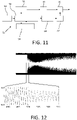
- a block diagram of the overall DDS-TF system 50 is shown in FIG. 11 .
- the input 52 is ⁇ fi, f 2 ,t ⁇ where f 1 is the start frequency, f 2 is the end frequency and t is the time of frequency transition.
- This goes into the DDS stepping algorithm 54 that also draws parameter data from the stored calibration tables 56 that were previously populated during on the calibration procedure discussed above in the TF frequency shifting calibration procedure discussed above.
- the conventional DDS function (DDS stepping algorithm 54, DDS ROM 58 and DAC 60) may be tightly coupled with TF 14. Additionally, a synchronous TF control DAC 62 and TF 14 may be implemented. With this tight coupling, DDS stepping algorithm 54 may be used to coordinate the control of both the DDS digital sequence generation as well as the TF frequency control 64 (generally in the form of a DAC analog bias voltage that controls the varactor diode).
- FIG. 13 shows the result after some iterative tuning, where values of the two phases were taken to determine where a continuous signal was achieved without interruption due to elimination of the transient that was observed in the non-tuned FIG. 12 example.
- These graphs depict a near instant change from f 1 to f 2 that is continuously filtered by the resonator.
- the RF frequency will transition between f 1 and f 2 .
- the bias voltage transition initiation time is accurately known, the instantaneous frequency and phase will be known throughout the transition.
- the change in bias voltage and hence the change in the capacitance will occur continuously and not just at the zero crossings of the capacitor voltage. The consequence of this is that the energy added to or subtracted from the resonator energy will be modulated.
- the phase of the f 2 signal and the energy may be known, and therefore the DDS amplitude and phase to synchronize with this residual signal is also known. Thereby it is possible to facilitate a smooth frequency transition from f 1 to f 2 wherein the frequency changes during the transition period are predictable and without further transition distortions after the start of the f 2 epoch.
- a calibration circuit is shown that may be used to calibrate the DDS 12 and TF 14 directly.
- the calibration may start with the range of frequencies that is anticipated.
- DDS 12 is shown with first and second DACs 60a and 60b. With the additional DAC channel, the DDS 12 may be used to generate a pair of outputs at a given frequency that are separated by 90 degrees.
- the outputs of the DDS 12 and TF 14 may be compared using multipliers 65 and a low pass filter and sampling block 67. With these, the response of TF 14 to the DDS stimulation at the set of calibration frequencies can be determined as a complex phasor.
- the TF response may be optimized for each frequency for a given target Q. These control voltages are noted along with the magnitude and phase shift of the response. In this way the TF transfer function may be characterized as a function of the control voltages.
- the DDS output is a sinusoidal signal with a frequency that changes instantaneously from f 1 to f 2 during P 1 and is constant at f 2 during P 2 .
- the periods of 1/ f 1 and 1/ f 2 are both short relative to the interval of P 1 or P 2 , it is meaningful to generate the quadrature component of the DDS over P 1 and P 2 .
- the TF output may then be demodulated in terms of these quadrature DDS generated components. This results in a sequence of complex valued phasor samples that can be analyzed in terms of phase and amplitude distortions of the TF output.
- the DDS output is fully deterministic, and in quadrature, such that from the complex phasor measurements it is possible to reconstruct the TF output in both P 1 and P 2 intervals. This can then be compared with the desired output from which the fitness of the parameters can be quantified.
- the DAC control voltages, phase of the f 1 at the transition point and phase of f 2 as it starts can be set to minimize the transient response.
- the DDS 12 can then generate the f 1 to f 2 transition and the actual transition measured based on the low pass filtering and sampling feedback. There can then be an iterative optimization loop where parameters of the DDS stepping algorithm can be optimized. Once complete, these parameters are stored in the calibration tables.
- a current DDS may be clocked at a rate of several GHz so that the DAC may read out new samples every few hundred picoseconds. All that is required of the DDS is to synthesize a DAC analog voltage output that drives the TF bias voltages and the RF input. Hence the resolution of the control input to the TF may be sub-nanoseconds.
- the DDS-TF control may be open loop during run time, during calibration, this control loop is sensed and then calibration tables may be updated. Ultimately the calibration table output may generate the sequence of digital samples required for the DDS to execute the upcoming f 1 to f 2 event. As such, the procedure may be implemented without additional functionality of the DDS.
- the calibration procedure detects the end phase of f 1 and the start phase of f 2 . Additionally, the total transition period of T s may be adjusted as the tightly coupled DDS will control the DAC to set the varactor bias voltage directly. The calibration circuit of FIG. 14 may then be used to determine the optimum set of parameters to facilitate the transition from f 1 to f 2 and thereby eliminate P 2 .
- the set of parameters may be determined as:
- the objective function of the calibration optimization is based on the desire to transition from f 1 to f 2 with the interval of P 1 + P 2 minimized.
- phase and frequency distortions typically degrade the coherency of the RF processing.
- P 1 and P 2 are variables, and it may be advantageous to increase P 1 slightly to achieve a reduction in P 2 .
- the load resistance limits the Q of the resonator.
- the active feedback bandpass filter can be represented by the simple resonator with a higher Q.
- R is the parallel resistance of the resonator which represents the finite Q of the resonator and the losses.
- the signal amplitude out of the DDS may be adjusted to achieve constant amplitude which might not be convenient, as a result of a design trade.
- a transition from an initial frequency of f 1 to a final frequency of f 2 may be considered. This has led to method of optimizing the transition by reducing P 2 towards zero, and by constraining the amplitude to be constant throughout the transition interval to take the P 2 transition period to zero.
- the DDS-TF are required to perform a finite number of such transitions, then calibration may be done for each f 1 to f 2 pair.
- this set of frequency pairs can grow to a large enough number that pairwise calibration is inconvenient.
- the calibrations may be very similar and therefore a set of empirical relations can be abstracted out of the set of pairwise calibrations.
- the multiple points 66 of calibration generally correspond to the varactor bias voltage time constant, which correspond with intermediate states that may be used during normal operation to minimize transition times from f 1 to f 2 . This may depend on a given implementation or application. Considerations of the application-specific calibrations is beyond the scope of the present discussion.
- transition period of P 1 is generally considered a nuisance but in other applications, a calibrated linear frequency chirp, or more generally a general frequency modulation, may be required from the DDS.
- P 1 interval can be expanded to include either a linear frequency chirp or a general frequency modulation.
Landscapes
- Engineering & Computer Science (AREA)
- Theoretical Computer Science (AREA)
- Physics & Mathematics (AREA)
- General Engineering & Computer Science (AREA)
- General Physics & Mathematics (AREA)
- Stabilization Of Oscillater, Synchronisation, Frequency Synthesizers (AREA)
- Inductance-Capacitance Distribution Constants And Capacitance-Resistance Oscillators (AREA)
Applications Claiming Priority (1)
| Application Number | Priority Date | Filing Date | Title |
|---|---|---|---|
| US202163187854P | 2021-05-12 | 2021-05-12 |
Publications (1)
| Publication Number | Publication Date |
|---|---|
| EP4089920A1 true EP4089920A1 (fr) | 2022-11-16 |
Family
ID=81648095
Family Applications (1)
| Application Number | Title | Priority Date | Filing Date |
|---|---|---|---|
| EP22172974.2A Pending EP4089920A1 (fr) | 2021-05-12 | 2022-05-12 | Commutation de fréquence rapide dans un filtre rf variable |
Country Status (2)
| Country | Link |
|---|---|
| US (1) | US12348208B2 (fr) |
| EP (1) | EP4089920A1 (fr) |
Citations (5)
| Publication number | Priority date | Publication date | Assignee | Title |
|---|---|---|---|---|
| US6420916B1 (en) * | 1997-08-05 | 2002-07-16 | Rockwell Collins, Inc. | Phase locked loop filter utilizing a tuned filter |
| EP1675263A1 (fr) * | 2004-12-23 | 2006-06-28 | Lucent Technologies Inc. | Réglage du facteur qualité (Q) d'un filtre |
| US9083351B1 (en) * | 2013-03-11 | 2015-07-14 | Raytheon Company | Phase lock loop with tracking filter for attenuating spurious signals of a swept local oscillator |
| US10050604B2 (en) | 2015-11-23 | 2018-08-14 | Aniotek Limited | Variable filter |
| US20210067125A1 (en) * | 2019-09-03 | 2021-03-04 | Anlotek Limited | Fast frequency switching in a resonant high-q analog filter |
Family Cites Families (92)
| Publication number | Priority date | Publication date | Assignee | Title |
|---|---|---|---|---|
| US1570771A (en) | 1922-03-20 | 1926-01-26 | American Telephone & Telegraph | Means for and method of reducing interference |
| US1778085A (en) | 1926-11-24 | 1930-10-14 | American Telephone & Telegraph | Distortionless amplifying system |
| US1915440A (en) | 1930-05-01 | 1933-06-27 | American Telephone & Telegraph | Regenerative amplifier |
| US1926169A (en) | 1931-03-11 | 1933-09-12 | American Telephone & Telegraph | Phase and frequency control |
| US2099769A (en) | 1936-06-23 | 1937-11-23 | American Telephone & Telegraph | Circuits embodying negative impedance |
| US3720881A (en) | 1972-01-17 | 1973-03-13 | Kinetic Technology Inc | Filter network having negative feedback loops |
| EP0420974B1 (fr) | 1989-04-21 | 1995-10-25 | Koninklijke Philips Electronics N.V. | Amplificateur a circuits accordes |
| US5311198A (en) | 1990-08-23 | 1994-05-10 | The United States Of America As Represented By The Administrator Of The National Aeronautics And Space Administration | Active antenna |
| US5291159A (en) | 1992-07-20 | 1994-03-01 | Westinghouse Electric Corp. | Acoustic resonator filter with electrically variable center frequency and bandwidth |
| US5491604A (en) | 1992-12-11 | 1996-02-13 | The Regents Of The University Of California | Q-controlled microresonators and tunable electronic filters using such resonators |
| US5854593A (en) | 1996-07-26 | 1998-12-29 | Prince Corporation | Fast scan trainable transmitter |
| US5917387A (en) | 1996-09-27 | 1999-06-29 | Lucent Technologies Inc. | Filter having tunable center frequency and/or tunable bandwidth |
| US5949290A (en) | 1997-01-14 | 1999-09-07 | Bertram; Earnest L. | Voltage controlled oscillator tuning apparatus and method |
| CA2224261A1 (fr) | 1997-12-09 | 1999-06-09 | Philsar Electronics Inc. | Amplificateur a faible bruit de phase, a facteur q eleve et a gain eleve dans un circuit integre |
| US6347237B1 (en) | 1999-03-16 | 2002-02-12 | Superconductor Technologies, Inc. | High temperature superconductor tunable filter |
| US6420913B1 (en) | 1999-09-20 | 2002-07-16 | Sun Microsystems, Inc. | Dynamic termination logic driver with improved impedance control |
| US6356143B2 (en) | 1999-11-01 | 2002-03-12 | Intreon Corporation | Method and apparatus for filtering radio frequency signals |
| GB0003313D0 (en) | 2000-02-15 | 2000-04-05 | Koninkl Philips Electronics Nv | Software reconfiguration of communications apparatus |
| US6920315B1 (en) | 2000-03-22 | 2005-07-19 | Ericsson Inc. | Multiple antenna impedance optimization |
| DE60116111T2 (de) | 2000-05-16 | 2006-11-02 | Chandler, Stephen Antony Gerard, Stroud | Rückgekoppelte hochfrequenzverstärker |
| US6452465B1 (en) | 2000-06-27 | 2002-09-17 | M-Squared Filters, Llc | High quality-factor tunable resonator |
| US6937877B2 (en) | 2000-12-21 | 2005-08-30 | General Electric Company | Wireless communication with a mobile asset employing dynamic configuration of a software defined radio |
| FI110868B (fi) | 2001-01-22 | 2003-04-15 | Maa Ja Elintarviketalouden Tut | Menetelmä sekoisolarisiresinolidiglykosidin (SDG) eristämiseksi ja puhdistamiseksi pellavansiemenistä |
| US6496075B2 (en) | 2001-03-14 | 2002-12-17 | Ericsson Inc. | Automatic tuning of VCO |
| US7174147B2 (en) | 2001-04-11 | 2007-02-06 | Kyocera Wireless Corp. | Bandpass filter with tunable resonator |
| JP3880329B2 (ja) | 2001-04-20 | 2007-02-14 | 株式会社日立国際電気 | ループゲイン制御方法及び電力増幅回路 |
| EP1251635A1 (fr) | 2001-04-20 | 2002-10-23 | Semiconductor Ideas to The Market (ItoM) BV | Amplificateur à résonance accordable |
| US6650195B1 (en) | 2001-07-30 | 2003-11-18 | Xilinx, Inc. | Oscillator with differential tunable tank circuit |
| US7151925B2 (en) | 2001-09-10 | 2006-12-19 | Industrial Technology Research Institute | Software defined radio (SDR) architecture for wireless digital communication systems |
| US6587007B2 (en) | 2001-11-26 | 2003-07-01 | Micrel, Incorporated | Ring topology based voltage controlled oscillator |
| US6771147B2 (en) | 2001-12-17 | 2004-08-03 | Remec, Inc. | 1-100 GHz microstrip filter |
| US6954774B1 (en) | 2001-12-20 | 2005-10-11 | Rockwell Collins | Bandpass filter with ability to tune a pass frequency, passband gain and filter Q |
| US7302237B2 (en) * | 2002-07-23 | 2007-11-27 | Mercury Computer Systems, Inc. | Wideband signal generators, measurement devices, methods of signal generation, and methods of signal analysis |
| DE10325396A1 (de) | 2003-05-28 | 2004-12-23 | Atmel Germany Gmbh | Schaltungsanordnung und Verfahren zur Phasenmodulation für rückstreubasierte Transponder |
| GB2403086B (en) | 2003-06-17 | 2005-07-20 | Motorola Inc | Cartesian loop transmitter and method of adjusting an output level of such transmitter |
| JP3931163B2 (ja) | 2003-08-14 | 2007-06-13 | 松下電器産業株式会社 | アンテナ整合装置 |
| FR2864727B1 (fr) | 2003-12-29 | 2007-05-11 | St Microelectronics Sa | Circuit electronique comportant un resonateur destine a etre integre dans un produit semi-conducteur |
| DE102004028068A1 (de) | 2004-06-09 | 2005-12-29 | Epcos Ag | Oszillator |
| US7098751B1 (en) | 2004-08-27 | 2006-08-29 | National Semiconductor Corporation | Tunable capacitance circuit for voltage control oscillator |
| JP4453575B2 (ja) | 2004-09-07 | 2010-04-21 | 株式会社日立製作所 | ソフトウェア無線装置 |
| US7522016B2 (en) | 2004-09-15 | 2009-04-21 | Qualcomm, Incorporated | Tunable surface acoustic wave resonators |
| US7433668B2 (en) | 2004-12-23 | 2008-10-07 | Lucent Technologies Inc. | Controlling Q-factor of filters |
| US7414779B2 (en) | 2005-01-20 | 2008-08-19 | Massachusetts Institute Of Technology | Mode locking methods and apparatus |
| JP4922677B2 (ja) | 2005-07-01 | 2012-04-25 | パナソニック株式会社 | 無線通信装置 |
| US7509141B1 (en) | 2005-09-29 | 2009-03-24 | Rockwell Collins, Inc. | Software defined radio computing architecture |
| US7809410B2 (en) | 2005-11-15 | 2010-10-05 | Harris Corporation | Power management system for SCA based software defined radio and related method |
| KR100735420B1 (ko) | 2006-02-17 | 2007-07-04 | 삼성전기주식회사 | 클럭 노이즈 제거 회로 |
| US7400203B2 (en) | 2006-08-03 | 2008-07-15 | Broadcom Corporation | Circuit with Q-enhancement cell having feedback loop |
| KR100921383B1 (ko) | 2006-09-08 | 2009-10-14 | 가부시키가이샤 엔.티.티.도코모 | 가변 공진기, 대역폭 가변 필터, 전기회로 장치 |
| JP4724135B2 (ja) | 2007-02-22 | 2011-07-13 | 株式会社エヌ・ティ・ティ・ドコモ | 可変共振器、可変フィルタ、電気回路装置 |
| US7937076B2 (en) | 2007-03-07 | 2011-05-03 | Harris Corporation | Software defined radio for loading waveform components at runtime in a software communications architecture (SCA) framework |
| US8050708B2 (en) | 2007-04-12 | 2011-11-01 | Harris Corporation | Option management in a software-defined radio |
| EP2168202B1 (fr) | 2007-06-27 | 2013-07-31 | Superconductor Technologies, Inc. | Filtre de radiofréquence pouvant être syntonisé de faible perte |
| DE602008004142D1 (de) | 2007-06-29 | 2011-02-03 | Thomson Licensing | Igitale fernsehsignale |
| FR2920927B1 (fr) | 2007-09-11 | 2011-05-06 | Commissariat Energie Atomique | Procede d'adaptation automatique d'impedance de circuit radiofrequence et chaine d'emission ou reception a adaptation automatique |
| US8107939B2 (en) | 2007-12-14 | 2012-01-31 | Microsoft Corporation | Software defined radio architecture |
| US7917117B2 (en) | 2008-01-28 | 2011-03-29 | University Of Washington | Auto-tuning amplifier |
| JP5417346B2 (ja) | 2008-02-28 | 2014-02-12 | ペレグリン セミコンダクター コーポレーション | 集積回路素子内でキャパシタをデジタル処理で同調するときに用いられる方法及び装置 |
| US8913652B2 (en) | 2008-03-10 | 2014-12-16 | Newlans, Inc. | Method, system and apparatus for wideband signal processing |
| US8120536B2 (en) | 2008-04-11 | 2012-02-21 | Powerwave Technologies Sweden Ab | Antenna isolation |
| US7884680B2 (en) | 2008-06-30 | 2011-02-08 | Infineon Technologies Ag | Dynamically adjustable Q-factors |
| US8103213B2 (en) | 2008-09-03 | 2012-01-24 | Nokia Corporation | Software-defined radio configuration |
| US9024709B2 (en) | 2008-10-03 | 2015-05-05 | Purdue Research Foundation | Tunable evanescent-mode cavity filter |
| US7994870B2 (en) | 2008-10-20 | 2011-08-09 | Qualcomm, Incorporated | Tunable filter with gain control circuit |
| FR2939581B1 (fr) | 2008-12-09 | 2010-11-26 | Commissariat Energie Atomique | Reseau de resonateurs couples, filtre passe-bande et oscillateur. |
| US8362853B2 (en) | 2009-06-19 | 2013-01-29 | Qualcomm Incorporated | Tunable MEMS resonators |
| US9166564B2 (en) | 2010-02-04 | 2015-10-20 | Hittite Microwave Corporation | Wideband analog bandpass filter |
| US20130065542A1 (en) | 2010-02-16 | 2013-03-14 | Cavitid, Inc., | Spectral Filtering Systems |
| US20110212692A1 (en) | 2010-02-26 | 2011-09-01 | Intersil Americas Inc. | Cascaded Filter Based Noise and Interference Canceller |
| GB2478585A (en) | 2010-03-11 | 2011-09-14 | Stephen Anthony Gerard Chandler | An RF amplifier linearised by RF feedback, and having a loop filter resonator of enhanced Q |
| CN102098018A (zh) | 2011-03-10 | 2011-06-15 | 江苏苏美达机电有限公司 | 一种可调带通滤波器系统 |
| US8767871B2 (en) | 2011-06-08 | 2014-07-01 | Broadcom Corporation | Antenna tuning using the ratio of complex forward and reflected signals |
| US9407239B2 (en) | 2011-07-06 | 2016-08-02 | Hrl Laboratories, Llc | Wide bandwidth automatic tuning circuit |
| GB2494652A (en) | 2011-09-14 | 2013-03-20 | Stephen Anthony Gerard Chandler | A transmitter amplifier with linearising RF feedback and automatic control of resonator Q, resonator frequency, loop phase, and loop gain |
| US9236846B2 (en) | 2011-12-06 | 2016-01-12 | Futurewei Technologies, Inc. | Tunable bandpass filter device and method |
| US8941441B2 (en) | 2013-03-15 | 2015-01-27 | Innophase Inc. | LNA with linearized gain over extended dynamic range |
| US8766712B2 (en) | 2012-05-04 | 2014-07-01 | Analog Devices, Inc. | Quality factor tuning for LC circuits |
| JP5618027B2 (ja) | 2012-09-28 | 2014-11-05 | 株式会社村田製作所 | インピーダンス変換回路およびアンテナ装置 |
| US9184498B2 (en) | 2013-03-15 | 2015-11-10 | Gigoptix, Inc. | Extending beamforming capability of a coupled voltage controlled oscillator (VCO) array during local oscillator (LO) signal generation through fine control of a tunable frequency of a tank circuit of a VCO thereof |
| US9484879B2 (en) | 2013-06-06 | 2016-11-01 | Qorvo Us, Inc. | Nonlinear capacitance linearization |
| WO2014181569A1 (fr) | 2013-05-10 | 2014-11-13 | 株式会社村田製作所 | Appareil d'antenne |
| US10228927B2 (en) | 2014-05-02 | 2019-03-12 | Neo Sastech Co., Ltd. | Method for distributing, installing, and executing software-defined radio application |
| WO2015176041A1 (fr) | 2014-05-15 | 2015-11-19 | The Regents Of The University Of California | Système résonateur actif avec facteur de qualité, fréquence et impédance accordables |
| US9813033B2 (en) | 2014-09-05 | 2017-11-07 | Innophase Inc. | System and method for inductor isolation |
| US9735752B2 (en) | 2014-12-03 | 2017-08-15 | Tdk Corporation | Apparatus and methods for tunable filters |
| CN104538714B (zh) | 2014-12-25 | 2017-04-26 | 深圳顺络电子股份有限公司 | 一种中心频率可调的带通滤波器 |
| EP3062442B1 (fr) | 2015-02-27 | 2019-01-16 | Friedrich-Alexander-Universität Erlangen-Nürnberg | Filtrage actif récursif hybride avec capacité de mise en forme adaptative de fonction de transfert |
| US9641138B2 (en) | 2015-04-09 | 2017-05-02 | Analog Devices, Inc. | Multipath feedforward band pass amplifier |
| WO2017122052A1 (fr) | 2016-01-15 | 2017-07-20 | Telefonaktiebolaget Lm Ericsson (Publ) | Filtres accordables miniatures |
| US10396807B1 (en) | 2016-02-08 | 2019-08-27 | Auburn University | Multi-ring coupled ring oscillator with improved phase noise |
| CN117318668A (zh) | 2017-05-24 | 2023-12-29 | 安乐泰克有限公司 | 用于控制谐振器的装置和方法 |
| US10236899B1 (en) | 2018-02-22 | 2019-03-19 | Allegro Microsystems, Llc | Tunable fractional phase locked loop |
-
2022
- 2022-05-12 EP EP22172974.2A patent/EP4089920A1/fr active Pending
- 2022-05-12 US US17/743,387 patent/US12348208B2/en active Active
Patent Citations (5)
| Publication number | Priority date | Publication date | Assignee | Title |
|---|---|---|---|---|
| US6420916B1 (en) * | 1997-08-05 | 2002-07-16 | Rockwell Collins, Inc. | Phase locked loop filter utilizing a tuned filter |
| EP1675263A1 (fr) * | 2004-12-23 | 2006-06-28 | Lucent Technologies Inc. | Réglage du facteur qualité (Q) d'un filtre |
| US9083351B1 (en) * | 2013-03-11 | 2015-07-14 | Raytheon Company | Phase lock loop with tracking filter for attenuating spurious signals of a swept local oscillator |
| US10050604B2 (en) | 2015-11-23 | 2018-08-14 | Aniotek Limited | Variable filter |
| US20210067125A1 (en) * | 2019-09-03 | 2021-03-04 | Anlotek Limited | Fast frequency switching in a resonant high-q analog filter |
Also Published As
| Publication number | Publication date |
|---|---|
| US12348208B2 (en) | 2025-07-01 |
| US20220376671A1 (en) | 2022-11-24 |
Similar Documents
| Publication | Publication Date | Title |
|---|---|---|
| CN101421928B (zh) | Vco驱动电路以及频率合成器 | |
| CN101569103B (zh) | 频率合成器和由该合成器生成期望频率的输出信号的方法 | |
| KR102427375B1 (ko) | 넓은 대역폭을 갖는 위상 동기 루프 회로 | |
| EP1982410B1 (fr) | Egalisation du gain d'un oscillateur | |
| EP2157690B1 (fr) | Procédé, système et appareil pour oscillateurs de référence stables à base de CL | |
| EP2144370A1 (fr) | Réduction de bruit de phase d'oscillateur par un réglage automatique du filtre et réponse sonore | |
| IL96351A (en) | Frequency synthesizer having microcomputer supplying analog and digital control signals to vco | |
| JPS63219225A (ja) | クロック信号発生器 | |
| EP3048722A1 (fr) | Systèmes et procédés d'étalonnage d'une boucle à verrouillage de phase à double port | |
| CN101371439A (zh) | 相位比较电路及使用该相位比较电路的pll频率合成器 | |
| US7492195B1 (en) | Agile, low phase noise clock synthesizer and jitter attenuator | |
| TW201914215A (zh) | 控制數位控制振盪器的方法 | |
| EP4089920A1 (fr) | Commutation de fréquence rapide dans un filtre rf variable | |
| CN112425077A (zh) | 直接调制合成器的高级多增益校准 | |
| EP4288794A1 (fr) | Systèmes et procédés de génération de modulation de fréquence de signal numérique à l'aide de multiplicateurs de fréquence | |
| EP1831988B1 (fr) | Oscillateur differentiel a alimentation en energie pulsee et methode de commande connexe | |
| US12283962B2 (en) | Method of controlling a frequency-modulated oscillator of a phase-locked loop circuit | |
| RU104798U1 (ru) | Генератор пав | |
| US7911283B1 (en) | Low noise oscillator and method | |
| US7054773B2 (en) | Dynamic model-based compensated tuning of a tunable device | |
| Humood et al. | Design LC oscillator for MF, HF& VHF using both ideal and practical operation amplifier | |
| JP3144501B2 (ja) | 周波数シンセサイザ | |
| RU2295825C1 (ru) | Частотно-модулированный генератор | |
| McKone et al. | Direct design approach for virtual oscillator control synchronisation condition & parameter selection using describing functions | |
| JP4805706B2 (ja) | 恒温型の水晶発振器 |
Legal Events
| Date | Code | Title | Description |
|---|---|---|---|
| PUAI | Public reference made under article 153(3) epc to a published international application that has entered the european phase |
Free format text: ORIGINAL CODE: 0009012 |
|
| STAA | Information on the status of an ep patent application or granted ep patent |
Free format text: STATUS: THE APPLICATION HAS BEEN PUBLISHED |
|
| AK | Designated contracting states |
Kind code of ref document: A1 Designated state(s): AL AT BE BG CH CY CZ DE DK EE ES FI FR GB GR HR HU IE IS IT LI LT LU LV MC MK MT NL NO PL PT RO RS SE SI SK SM TR |
|
| STAA | Information on the status of an ep patent application or granted ep patent |
Free format text: STATUS: REQUEST FOR EXAMINATION WAS MADE |
|
| 17P | Request for examination filed |
Effective date: 20230515 |
|
| RBV | Designated contracting states (corrected) |
Designated state(s): AL AT BE BG CH CY CZ DE DK EE ES FI FR GB GR HR HU IE IS IT LI LT LU LV MC MK MT NL NO PL PT RO RS SE SI SK SM TR |
|
| STAA | Information on the status of an ep patent application or granted ep patent |
Free format text: STATUS: EXAMINATION IS IN PROGRESS |
|
| 17Q | First examination report despatched |
Effective date: 20250422 |