EP0421403A2 - Lichtempfangende Vorrichtung - Google Patents
Lichtempfangende Vorrichtung Download PDFInfo
- Publication number
- EP0421403A2 EP0421403A2 EP90119004A EP90119004A EP0421403A2 EP 0421403 A2 EP0421403 A2 EP 0421403A2 EP 90119004 A EP90119004 A EP 90119004A EP 90119004 A EP90119004 A EP 90119004A EP 0421403 A2 EP0421403 A2 EP 0421403A2
- Authority
- EP
- European Patent Office
- Prior art keywords
- light
- active area
- receiving element
- signal
- output
- Prior art date
- Legal status (The legal status is an assumption and is not a legal conclusion. Google has not performed a legal analysis and makes no representation as to the accuracy of the status listed.)
- Withdrawn
Links
- 230000003287 optical effect Effects 0.000 claims abstract description 20
- 230000005540 biological transmission Effects 0.000 abstract description 10
- 239000004065 semiconductor Substances 0.000 description 12
- VYPSYNLAJGMNEJ-UHFFFAOYSA-N Silicium dioxide Chemical compound O=[Si]=O VYPSYNLAJGMNEJ-UHFFFAOYSA-N 0.000 description 9
- 239000002184 metal Substances 0.000 description 5
- 239000013307 optical fiber Substances 0.000 description 5
- 229910052681 coesite Inorganic materials 0.000 description 4
- 229910052906 cristobalite Inorganic materials 0.000 description 4
- 238000010586 diagram Methods 0.000 description 4
- 239000000377 silicon dioxide Substances 0.000 description 4
- 235000012239 silicon dioxide Nutrition 0.000 description 4
- 229910052682 stishovite Inorganic materials 0.000 description 4
- 229910052905 tridymite Inorganic materials 0.000 description 4
- 238000012986 modification Methods 0.000 description 2
- 230000004048 modification Effects 0.000 description 2
- 239000003990 capacitor Substances 0.000 description 1
- 239000000835 fiber Substances 0.000 description 1
- 230000012447 hatching Effects 0.000 description 1
- 238000012544 monitoring process Methods 0.000 description 1
- 230000005855 radiation Effects 0.000 description 1
- 230000035945 sensitivity Effects 0.000 description 1
- 229910052814 silicon oxide Inorganic materials 0.000 description 1
Images


Classifications
-
- H—ELECTRICITY
- H04—ELECTRIC COMMUNICATION TECHNIQUE
- H04B—TRANSMISSION
- H04B10/00—Transmission systems employing electromagnetic waves other than radio-waves, e.g. infrared, visible or ultraviolet light, or employing corpuscular radiation, e.g. quantum communication
- H04B10/60—Receivers
- H04B10/66—Non-coherent receivers, e.g. using direct detection
-
- H—ELECTRICITY
- H10—SEMICONDUCTOR DEVICES; ELECTRIC SOLID-STATE DEVICES NOT OTHERWISE PROVIDED FOR
- H10F—INORGANIC SEMICONDUCTOR DEVICES SENSITIVE TO INFRARED RADIATION, LIGHT, ELECTROMAGNETIC RADIATION OF SHORTER WAVELENGTH OR CORPUSCULAR RADIATION
- H10F30/00—Individual radiation-sensitive semiconductor devices in which radiation controls the flow of current through the devices, e.g. photodetectors
- H10F30/20—Individual radiation-sensitive semiconductor devices in which radiation controls the flow of current through the devices, e.g. photodetectors the devices having potential barriers, e.g. phototransistors
- H10F30/21—Individual radiation-sensitive semiconductor devices in which radiation controls the flow of current through the devices, e.g. photodetectors the devices having potential barriers, e.g. phototransistors the devices being sensitive to infrared, visible or ultraviolet radiation
- H10F30/22—Individual radiation-sensitive semiconductor devices in which radiation controls the flow of current through the devices, e.g. photodetectors the devices having potential barriers, e.g. phototransistors the devices being sensitive to infrared, visible or ultraviolet radiation the devices having only one potential barrier, e.g. photodiodes
- H10F30/223—Individual radiation-sensitive semiconductor devices in which radiation controls the flow of current through the devices, e.g. photodetectors the devices having potential barriers, e.g. phototransistors the devices being sensitive to infrared, visible or ultraviolet radiation the devices having only one potential barrier, e.g. photodiodes the potential barrier being a PIN barrier
-
- H—ELECTRICITY
- H10—SEMICONDUCTOR DEVICES; ELECTRIC SOLID-STATE DEVICES NOT OTHERWISE PROVIDED FOR
- H10F—INORGANIC SEMICONDUCTOR DEVICES SENSITIVE TO INFRARED RADIATION, LIGHT, ELECTROMAGNETIC RADIATION OF SHORTER WAVELENGTH OR CORPUSCULAR RADIATION
- H10F39/00—Integrated devices, or assemblies of multiple devices, comprising at least one element covered by group H10F30/00, e.g. radiation detectors comprising photodiode arrays
- H10F39/10—Integrated devices
- H10F39/103—Integrated devices the at least one element covered by H10F30/00 having potential barriers, e.g. integrated devices comprising photodiodes or phototransistors
Definitions
- the present invention relates to a light-receiving element used in, e.g., an optical communication system such as an optical LAN(local area network) or an optical CATV system.
- an optical communication system such as an optical LAN(local area network) or an optical CATV system.
- a light signal receiving section in an optical communication system of this type generally employs a circuit arrangement, as shown in Fig. 1.
- a light signal When a light signal is incident on a light-receiving element 1, the light-receiving element 1 generates a light output current.
- the light output current is converted into a voltage signal by a resistor 2, and the voltage signal is supplied to an amplifier 3.
- the incident light signal is amplified and demodulated by the amplifier 3, and the demodulated signal is output.
- the output signal from the amplifier 3 is also supplied to an amplifier 4.
- the output terminal of the amplifier 4 is connected to diodes 5 and 6, a resistor 7, and a capacitor 8.
- the output signal supplied to the amplifier 4 is output to a terminal 9 as a monitor signal.
- Most optical communication systems have a function of monitoring the presence/absence of a light input.
- Fig. 2A is a plan view of the light-receiving element 1
- Fig. 2B is a longitudinal sectional view of Fig. 2A.
- the light-receiving element 1 is formed to shave a PIN structure SiO2 (silicon oxide) film 10 is formed.
- a light signal emitting from an optical fiber is radiated on an active area 11 indicated by hatching in Fig. 2A.
- a metal wall 12 is formed around the active area 11.
- the PIN structure Upon radiation of the light signal, the PIN structure generates a light output current.
- the light output current is output through a lead terminal formed by the metal wall 12.
- the present invention has been made to solve the above problem, and has an object to provide a light- receiving element which can perform accurate information transmission even if a light signal is very weak.
- a light-receiving element is formed by comprising the first active area irradiated with a light signal, and the second active area irradiated with a leakage component of the light signal. For this reason, an output optical current for information transmission is generated by a light signal radiated on the first active area, and a monitor output optical current is generated by a leakage component of the light signal radiated on the second active area. Therefore, even if an incident light signal is very weak, as the monitor light output current is independently generated, no disturbance occurs in an output electrical signal for information transmission. Therefore, according to the present invention, information transmission in an optical communication system can be accurately performed.
- Figs. 3A and 3B show a structure of a PIN photodiode according to an embodiment of the present invention
- Fig. 3A is a plan view
- Fig. 3B is an enlarged longitudinal sectional view of Fig. 3A
- An intrinsic (i-type) semiconductor layer 22 is formed on an n+-type semiconductor layer 21, and p+-type semiconductor layers 23 and 24 are formed in a predetermined region in a surface portion of i-type semiconductor layer 22 to be electrically isolated from each other.
- An SiO2 film 25 is formed on the p+-type semiconductor layers 23 and 24, and a portion of the SiO2 film 25 on the predetermined region is removed. Electrically isolated metal walls 26 and 27 are formed on the removed portion to be in electrical contact with the p+-type semiconductor layers 23 and 24, thus forming two light-receiving surfaces 28 and 29. Portions of the metal walls 26 and 27 externally extend to form lead portions 26a and 27a.
- the SiO2 film 25 serves as an anti-refelection film of light radiated on the active area 28 and 29.
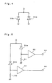
- Fig. 4 is an equivalent circuit diagram of a PIN photodiode 30 with the above structure.
- the PIN photodiode 30 is expressed as a parallel circuit of two PIN photodiodes 30a and 30b.
- the PIN photodiode 30a is constituted by the n+-type semiconductor layer 21, the i-type semiconductor layer 22, and the p+-type semiconductor layer 23, and its surface 28 serves as the active area.
- the PIN photodiode 30b is constituted by the n+-type semiconductor layer 21, the i-type semiconductor layer 22, and the p+-type semiconductor layer 24, and its surface 29 serves as the active area.
- a light signal is emitted from an optical fiber for transmitting light information toward the active area 28 located at a central portion.
- Most of the light signals are radiated on the active area 28, and its leakage light component is also radiated on the active area 29 located around the active area 28.
- the leakage light component means a light component which is not radiated on the active area 28 of light emitting from the optical fiber.
- a light output current for information transmission is generated by the light signal radiated on the active area 28, and a monitor output optical current is generated by the leakage light component of the light signal radiated on the active area 29.
- These output optical currents are output to an external circuit via the lead portions 26a and 27a of the metal walls 26 and 27.
- Fig. 5 shows a light-receiving circuit using this PIN photodiode 30.
- the cathodes of the PIN photodiodes 30a and 30b are electrically connected to each other, and are boosted to a power supply voltage of the circuit.
- the anodes of the PIN photodiodes 30a and 30b are grounded through resistors 31 and 32, respectively, and are also connected to the input terminals of amplifiers 33 and 34, respectively.
- the output terminals of the amplifiers 33 and 34 are respectively connected to terminals 35 and 36.
- a circuit constituted by the PIN photodiode 30a, the resistor 31, and the amplifier 33 is a normal light-receiving circuit. This light-receiving circuit is set to have a receiver bandwidth corresponding to a transmission speed of information.
- a circuit constituted by the PIN photodiode 30b, the resistor 32, and the amplifier 34 is a monitor circuit. Since this monitor circuit need only to detect an average level of a modulated light signal, it preferably has a large time constant.
- the resistor 32 preferably has a high resistance to get high sensitivity, and is set to be about 1 M ⁇ .
- an output optical current is generated by the PIN photodiode 30a, and is converted into a voltage signal by the resistor 31.
- the voltage signal is supplied to the amplifier 33.
- the signal received by the amplifier 33 is amplified, and information transmitted through the optical fiber is demodulated and output to the terminal 35.
- the leakage light component of the received light signal is radiated on the acive area 29, and an output optical current according to the leakage light component is generated by the PIN photodiode 30b.
- the output optical current is amplified by the amplifier 34, and is output to the terminal 36 as a monitor signal for determining the presence/absence of an input optical signal.
- a leakage light component which is not positively utilized and is not radiated on the active area 28 is received by the active area 29. For this reason, a light input can be monitored without giving a disturbance to a demodulated signal obtained from the amplifier 33.
- the main acitve area is formed into a circular shape
- said second active area 29 is formed around said first acitve area 28 into a circular shape concentrically with said first active area 28.
Landscapes
- Physics & Mathematics (AREA)
- Electromagnetism (AREA)
- Engineering & Computer Science (AREA)
- Computer Networks & Wireless Communication (AREA)
- Signal Processing (AREA)
- Light Receiving Elements (AREA)
- Optical Communication System (AREA)
Applications Claiming Priority (2)
| Application Number | Priority Date | Filing Date | Title |
|---|---|---|---|
| JP259829/89 | 1989-10-04 | ||
| JP1259829A JPH03120877A (ja) | 1989-10-04 | 1989-10-04 | 受光素子 |
Publications (2)
| Publication Number | Publication Date |
|---|---|
| EP0421403A2 true EP0421403A2 (de) | 1991-04-10 |
| EP0421403A3 EP0421403A3 (en) | 1992-03-18 |
Family
ID=17339571
Family Applications (1)
| Application Number | Title | Priority Date | Filing Date |
|---|---|---|---|
| EP19900119004 Withdrawn EP0421403A3 (en) | 1989-10-04 | 1990-10-04 | Light-receiving element |
Country Status (4)
| Country | Link |
|---|---|
| US (1) | US5164581A (de) |
| EP (1) | EP0421403A3 (de) |
| JP (1) | JPH03120877A (de) |
| CA (1) | CA2026861A1 (de) |
Cited By (3)
| Publication number | Priority date | Publication date | Assignee | Title |
|---|---|---|---|---|
| EP0875939A1 (de) * | 1997-04-30 | 1998-11-04 | Interuniversitair Micro-Elektronica Centrum Vzw | Räumlich modulierter Detektor für elektromagnetische Strahlung |
| EP0967663A3 (de) * | 1998-06-22 | 2000-01-26 | Sumitomo Electric Industries, Ltd. | Photodiode und Photodiodenmodul |
| EP0924771A4 (de) * | 1997-06-11 | 2000-07-26 | Seiko Epson Corp | Halbleiterbauelement, flüssigkristall-anzeigevorrichtung, und elektronisches gerät mit denselben |
Families Citing this family (6)
| Publication number | Priority date | Publication date | Assignee | Title |
|---|---|---|---|---|
| US5278397A (en) * | 1991-07-25 | 1994-01-11 | Symbol Technologies, Inc. | Multi-resolution bar code reader |
| US6213399B1 (en) | 1991-07-25 | 2001-04-10 | Symbol Technologies, Inc. | Multi-channel signal processing in an optical reader |
| US5767500A (en) * | 1996-02-06 | 1998-06-16 | Symbol Technologies, Inc. | Automatic identification of hardware |
| IT1290576B1 (it) * | 1997-03-07 | 1998-12-10 | Cise Spa | Dispositivo per la rilevazione di parametri ottici di un fascio laser |
| JP4068842B2 (ja) * | 1999-08-25 | 2008-03-26 | 浜松ホトニクス株式会社 | 光受信装置、並びに、その保持装置及び配置方法 |
| US6870152B2 (en) * | 2002-02-01 | 2005-03-22 | Georgia Tech Research Corporation | Segmented photodetectors for detection and compensation of modal dispersion in optical waveguides |
Family Cites Families (7)
| Publication number | Priority date | Publication date | Assignee | Title |
|---|---|---|---|---|
| US3777149A (en) * | 1972-07-17 | 1973-12-04 | Bell Telephone Labor Inc | Signal detection and delay equalization in optical fiber transmission systems |
| US3777150A (en) * | 1972-07-17 | 1973-12-04 | Bell Telephone Labor Inc | Mode detection and delay equalization in multimode optical fiber transmission systems |
| DE2853292A1 (de) * | 1978-11-24 | 1980-06-12 | Bbc Brown Boveri & Cie | Optisch aktivierbares halbleiterbauelement |
| US4366377A (en) * | 1980-09-29 | 1982-12-28 | Mcdonnell Douglas Corporation | Dual sensitivity optical sensor |
| GB2194111A (en) * | 1986-07-18 | 1988-02-24 | Gen Electric Plc | Optical signal receiver circuits |
| JPS63215942A (ja) * | 1987-03-04 | 1988-09-08 | Natl Aerospace Lab | 粒子径分布計測用光電変換センサ− |
| GB2212020B (en) * | 1987-11-03 | 1991-07-10 | Stc Plc | Optical detectors. |
-
1989
- 1989-10-04 JP JP1259829A patent/JPH03120877A/ja active Pending
-
1990
- 1990-09-27 US US07/588,854 patent/US5164581A/en not_active Expired - Fee Related
- 1990-10-03 CA CA002026861A patent/CA2026861A1/en not_active Abandoned
- 1990-10-04 EP EP19900119004 patent/EP0421403A3/en not_active Withdrawn
Cited By (7)
| Publication number | Priority date | Publication date | Assignee | Title |
|---|---|---|---|---|
| EP0875939A1 (de) * | 1997-04-30 | 1998-11-04 | Interuniversitair Micro-Elektronica Centrum Vzw | Räumlich modulierter Detektor für elektromagnetische Strahlung |
| US6157035A (en) * | 1997-04-30 | 2000-12-05 | Imec | Spatially modulated detector for radiation |
| EP0924771A4 (de) * | 1997-06-11 | 2000-07-26 | Seiko Epson Corp | Halbleiterbauelement, flüssigkristall-anzeigevorrichtung, und elektronisches gerät mit denselben |
| US6552712B1 (en) | 1997-06-11 | 2003-04-22 | Seiko Epson Corporation | Semiconductor device, liquid crystal display, and electronic equipment including the same |
| EP0967663A3 (de) * | 1998-06-22 | 2000-01-26 | Sumitomo Electric Industries, Ltd. | Photodiode und Photodiodenmodul |
| US6437415B1 (en) | 1998-06-22 | 2002-08-20 | Sumitomo Electric Industries, Ltd. | Photodiode and photodiode module |
| US6724063B2 (en) | 1998-06-22 | 2004-04-20 | Sumitomo Electric Industries, Ltd. | Photodiode and photodiode module |
Also Published As
| Publication number | Publication date |
|---|---|
| CA2026861A1 (en) | 1991-04-05 |
| JPH03120877A (ja) | 1991-05-23 |
| US5164581A (en) | 1992-11-17 |
| EP0421403A3 (en) | 1992-03-18 |
Similar Documents
| Publication | Publication Date | Title |
|---|---|---|
| US4954786A (en) | Optical amplifying device | |
| US4438348A (en) | Temperature compensated avalanche photodiode optical receiver circuit | |
| US4945229A (en) | Fiber optic receiver and transceiver | |
| US4284884A (en) | Electro-optic devices | |
| US4176367A (en) | Semiconductor optical device | |
| US6051967A (en) | Electric field measurement system | |
| EP0421403A2 (de) | Lichtempfangende Vorrichtung | |
| US6670600B2 (en) | Semiconductor photodetector with ohmic contact areas formed to prevent incident light from resolving the areas, semiconductor photo receiver and semiconductor device installed with the semiconductor photodetector | |
| AU637704B2 (en) | Photo detectors | |
| EP0080318B1 (de) | Optische Einrichtung zur Abfrage der Stellung eines Schalters | |
| EP0042158A2 (de) | Optokoppler zum Übertragen und Empfangen über eine optische Fiber | |
| US20050133695A1 (en) | Photodetector and optical receiver | |
| US3984824A (en) | Wide-band optical analog signal link using fiber optics | |
| US4754131A (en) | Devices using avalanche photodiode and capable of detecting a small number of photons | |
| US5150189A (en) | Semiconductor apparatus | |
| EP1014098B1 (de) | Gleichstrommessgerät mit passivem Eingang und mit galvanischer Isolierung, insbesondere für Hochspannung | |
| JP2004153190A (ja) | アバランシェフォトダイオードの製造方法ならびにアバランシェフォトダイオード、光受信モジュールおよび光受信装置 | |
| US5075794A (en) | Reflective opitical feedback element | |
| JPH065888A (ja) | 光検出装置及びそれを用いた電気機器の故障監視装置 | |
| GB2192510A (en) | Optical receiver | |
| GB2194406A (en) | Optical signal receiver circuits | |
| JPH06132899A (ja) | 光受信回路 | |
| SU1410944A1 (ru) | Устройство Ю.Бабича дл электрофизиологических исследований | |
| JPS59206733A (ja) | 高電位に接続して利用する真空機器の真空監視装置 | |
| CA1134933A (en) | Electro-optic devices |
Legal Events
| Date | Code | Title | Description |
|---|---|---|---|
| PUAI | Public reference made under article 153(3) epc to a published international application that has entered the european phase |
Free format text: ORIGINAL CODE: 0009012 |
|
| 17P | Request for examination filed |
Effective date: 19910102 |
|
| AK | Designated contracting states |
Kind code of ref document: A2 Designated state(s): DE FR GB NL SE |
|
| PUAL | Search report despatched |
Free format text: ORIGINAL CODE: 0009013 |
|
| AK | Designated contracting states |
Kind code of ref document: A3 Designated state(s): DE FR GB NL SE |
|
| 17Q | First examination report despatched |
Effective date: 19931020 |
|
| GRAG | Despatch of communication of intention to grant |
Free format text: ORIGINAL CODE: EPIDOS AGRA |
|
| STAA | Information on the status of an ep patent application or granted ep patent |
Free format text: STATUS: THE APPLICATION HAS BEEN WITHDRAWN |
|
| 18W | Application withdrawn |
Withdrawal date: 19960627 |