EP0421430B1 - Plasmaprozess, Verfahren und Gerät - Google Patents
Plasmaprozess, Verfahren und Gerät Download PDFInfo
- Publication number
- EP0421430B1 EP0421430B1 EP90119065A EP90119065A EP0421430B1 EP 0421430 B1 EP0421430 B1 EP 0421430B1 EP 90119065 A EP90119065 A EP 90119065A EP 90119065 A EP90119065 A EP 90119065A EP 0421430 B1 EP0421430 B1 EP 0421430B1
- Authority
- EP
- European Patent Office
- Prior art keywords
- plasma
- frequency
- power
- mhz
- plasma etching
- Prior art date
- Legal status (The legal status is an assumption and is not a legal conclusion. Google has not performed a legal analysis and makes no representation as to the accuracy of the status listed.)
- Expired - Lifetime
Links
Images

Classifications
-
- H—ELECTRICITY
- H01—ELECTRIC ELEMENTS
- H01J—ELECTRIC DISCHARGE TUBES OR DISCHARGE LAMPS
- H01J37/00—Discharge tubes with provision for introducing objects or material to be exposed to the discharge, e.g. for the purpose of examination or processing thereof
- H01J37/32—Gas-filled discharge tubes
- H01J37/32009—Arrangements for generation of plasma specially adapted for examination or treatment of objects, e.g. plasma sources
- H01J37/32082—Radio frequency generated discharge
- H01J37/32174—Circuits specially adapted for controlling the RF discharge
-
- H—ELECTRICITY
- H10—SEMICONDUCTOR DEVICES; ELECTRIC SOLID-STATE DEVICES NOT OTHERWISE PROVIDED FOR
- H10P—GENERIC PROCESSES OR APPARATUS FOR THE MANUFACTURE OR TREATMENT OF DEVICES COVERED BY CLASS H10
- H10P14/00—Formation of materials, e.g. in the shape of layers or pillars
- H10P14/20—Formation of materials, e.g. in the shape of layers or pillars of semiconductor materials
-
- H—ELECTRICITY
- H01—ELECTRIC ELEMENTS
- H01J—ELECTRIC DISCHARGE TUBES OR DISCHARGE LAMPS
- H01J37/00—Discharge tubes with provision for introducing objects or material to be exposed to the discharge, e.g. for the purpose of examination or processing thereof
- H01J37/32—Gas-filled discharge tubes
- H01J37/32009—Arrangements for generation of plasma specially adapted for examination or treatment of objects, e.g. plasma sources
- H01J37/32082—Radio frequency generated discharge
Definitions
- This invention relates a plasma etching method and a plasma etching apparatus for semiconductor wafer processing.
- Plasma etching of wafers is attractive because it can be anisotropic, can be chemically selective, can produce etch under conditions far from thermodynamic equilibrium, utilizes a reduced amount of etchant chemicals compared to wet etch processes and produces a significantly reduced amount of waste products.
- the reduction of etchant chemicals and waste products produces a cost savings.
- the anisotropic etch enables the production of substantially vertical sidewalls which is important in present day processes in which the depth of etch and feature size and spacing are all comparable.
- etch chemicals and process parameters to produce chemical selectivity of the etch enables these choices to be made to etch the desired material without substantially etching other features of the integrated circuits being produced.
- Choices of process parameters that produce process conditions far from thermodynamic equilibrium can be used to lower process temperature, thereby avoiding high temperatures that can deleteriously affect the integrated circuits under fabrication.
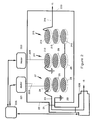
- FIG. 1 a plasma reactor 10.
- This reactor includes an aluminum wall 11 that encloses a plasma reactor chamber 12. Wall 11 is grounded and functions as one of the plasma electrodes. Gases are supplied to chamber 12 from a gas source 13 and are exhausted by an exhaust system 14 that actively pumps gases out of the reactor to maintain a low pressure suitable for a plasma process.
- An rf power supply 15 provides power to a second (powered) electrode 16 to generate a plasma within chamber 12. Wafers 17 are transferred into and out of reactor chamber 12 through a port such as slit valve 18.
- a plasma consists of two qualitatively different regions: the substantially neutral, conductive plasma body 19 and a boundary layer 110 called the plasma sheath.
- the plasma body consists of substantially equal densities of negative and positive charged particles as well as radicals and stable neutral particles.
- the plasma sheath is an electron deficient, poorly conductive region in which the electric field strength is large. The plasma sheath forms between the plasma body and any interface such as the walls and electrodes of the plasma reactor chamber and the rf electrodes.
- Semiconductor process plasmas are produced by a radio frequency (rf) field at 13.56 MHz that couples energy into free electrons within the chamber, imparting sufficient energy to many of these electrons that ions can be produced through collisions of these electrons with gas molecules.
- rf radio frequency
- the walls of the reactor chamber are metal (though often coated with thin insulating layers) so that they can function as one of the rf electrodes. When the walls do not function as one of the electrodes, they still affect the process by confining the plasma and by contributing capacitive coupling to the plasma reactor.
- the 13.56 MHz frequency is substantially universally utilized in plasma reactors because this frequency is an ISM (Industry, Scientific, Medical) standard frequency for which the government mandated radiation limits are less stringent than at non-ISM frequencies, particularly those within the communication bands. This substantial universal use of 13.56 MHz is further encouraged by the large amount of equipment available at that frequency because of this ISM standard. Other ISM standard frequencies are at 27.12 and 40.68 MHz, which are first and second order harmonics of the 13.56 MHz ISM standard frequency. A further advantage of the 13.56 MHz frequency is that, since the lowest two order harmonics of this frequency are also ISM standard frequencies, equipment utilizing 13.56 MHz is less likely to exceed allowable limits at harmonics of the fundamental frequency of such equipment.
- ISM Industry, Scientific, Medical
- a dc self bias V dc of this electrode results.
- the magnitude of this self bias V dc is a function of the ion density and electron temperature within the plasma.
- a negative self-bias dc voltage V dc of the powered electrode on the order of several hundreds of volts is commonly produced (see, for example, J. Coburn and E. Kay, Positive-ion bombardment of substrates in rf diode glow discharge sputtering , J. Appl. Phys., 43 , p. 4965 (1972).
- This self bias dc voltage V dc is useful in producing a high energy flux of positive ions against the powered electrode.
- a wafer 17 to be etched is positioned on or slightly above the powered electrode 16 so that this flux of positive ions is incident substantially perpendicular to the top surface of the wafer, thereby producing substantially vertical etching of unprotected regions of the wafer.
- the wafer throughput of the system is limited to the throughput of the slowest of the series of process steps within such a system, it is important that none of these sequential steps take significantly longer than the other steps in the process or else such slow step will serve as a bottleneck to system throughput.
- typical system throughput is on the order of 60 wafers per hour.
- the fundamental etch prior to metal 2 deposition is performed at a rate equivalent to 250.10 -9 m (250 Angstroms) per minute silicon dioxide etch rate. This permits the removal of approximately 70.10 -9 m (70 Angstroms) of aluminum oxide in contacts to aluminum metal 1 in approximately 40 seconds using a nonselective argon-only process. These etch conditions are used routinely in wafer fabrication and produce a 1500-1600 volt self bias at the powered electrode.
- One solution has been to enhance the etch rate by use of magnets that produce containment fields that trap ions within the vicinity of the wafer, thereby increasing the ion density at the wafer.
- the magnetic field confines energetic ions and electrons by forcing them to spiral along helical orbits about the magnetic field lines.
- Such increased ion density at the wafer produces a concomitant increase in etch rate without increasing the self bias potential, thereby enabling throughputs on the order of 60 wafers per hour without damaging the wafers.
- the etch rate is preserved by increasing the current level to counter the decreased voltage drop across the plasma sheath at the wafer.
- nonuniformities of the magnetic field of such "magnetically enhanced" plasma etching systems exhibit a decreased uniformity of etch rate over the surface of the wafer.
- the wafer is rotated about an axis that is perpendicular to and centered over the surface of the powered electrode. This produces at the wafer surface a time-averaged field that has cylindrical symmetry and an improved uniformity over the wafer and therefore produces increased etch uniformity over the surface of the wafer.
- this rotation produces within the plasma chamber undesirable mechanical motion that can produce particulates and increase contamination.
- a rotating magnetic field can be produced by use of two magnetic coils driven by currents that are ninety degrees out of phase.
- the controls and power supplies for this scheme are relatively expensive and the etch uniformity is still not as good as in a plasma etch apparatus that does not include such magnets.
- the invention provides a high frequency semiconductor wafer processing method and apparatus and relates more particularly to the use of a plasma apparatus for wafer etching.
- the invention provides a plasma etching method according to independent claim 1 and a plasma etching apparatus according to independent claim 9. Further advantageous features of the method and apparatus are evident from the dependent claims, 10 the description and the drawings. The claims are intended to be a first non-limiting approach of defining the invention in general terms.
- an igniter electrode produces, within a low pressure gas, high energy electrons that have enough energy to ionize within the reactor chamber atoms and molecules struck by these high energy electrons. This results in a cascade of electrons that produce a plasma consisting of electrons, ions, radicals and stable neutral particles.
- the plasma is then maintained by a powered electrode of voltage lower than that of the igniter electrode.
- Sufficient rf power is coupled into the plasma to maintain a desired ion concentration, typically on the order of 10 8 - 10 11 cm -3 .
- Typical the frequency of the rf power is in the range from 10 kHz to 30 MHz, but the most common frequency is 13.56 MHz because this is high enough to produce reasonable ion concentrations and is an ISM (industry, scientific, medical) standard frequency that does not interfere with telecommunications.
- the electrons are on the order of thousands to hundreds of thousands of times lighter than the plasma ions, the electrons experience a proportionately greater acceleration than the ions and therefore acquire kinetic energies that are significantly greater than those acquired by the ions.
- the effect of this is that the energy from the rf field is strongly coupled into electron kinetic energy and is only very weakly coupled into ion kinetic energy.
- These high energy electrons are also referred to as high temperature electrons.
- collisions between the high energy electrons and the ions does not transfer much of the electron energy to the ions.
- the electrons acquire a temperature that is typically on the order of 1-5 eV even though the other particles in the plasma remain substantially at the temperature of the walls of the plasma reactor chamber (on the order of 0.03 eV) or up to a few hundred °C (degrees Centigrade) hotter.
- the electrons are much more mobile than the ions, they initially strike the walls of the reactor chamber at a greater rate than do the ions.
- the effect of this is that the plasma body becomes slightly electron deficient while the boundary layer sheath becomes substantially electron deficient.
- This also produces a positively charged layer at the interface between the plasma body and the plasma sheath.
- This net positive charge of the plasma body and boundary layer results in a plasma body electrical potential V p (usually called the "plasma potential”) on the order of several times the electron mean kinetic energy divided by the electron charge.
- V p usually called the "plasma potential”
- the potential in the bulk of the plasma is nearly constant while the largest part of the potential variation is across the sheath.
- this sheath potential variation is also dependent on various parameters including the area of the reactor chamber wall, the area of the powered electrode, the pressure in the reactor chamber and the rf power input.
- a plasma apparatus that operates at frequencies higher than the 13.56 MHz frequency utilized in conventional plasma apparatus.
- Useful frequencies for plasma processing have been found to range from 30 to 200 MHz. These processes include various plasma etching processes. The frequency that is selected is dependent on which of these processes is being utilized which in turn determines the required choice of plasma density and ion bombardment energy.
- the lower frequency limit is controlled by the maximum self bias voltage that can be used without damaging the integrated circuit under fabrication.
- the upper frequency limit is controlled by the minimum self bias voltage (about 150 volts for a nonreactive etch process and 50 volts for a reactive ion etch process) that produces sufficient energy to etch the wafer.
- this upper limit is further reduced by the requirement that such etching be achievable within a period that is short enough that this etching step does not create a bottleneck to fabrication throughput.
- This range of frequencies has required modification of the match network that prevents reflections of rf power at the transition from the 50 ohm characteristic impedance of the rf transmission line to the much lower impedance of the plasma reactor chamber.
- the plasma is generated by detuning the match network to make the powered electrode function as an igniter and then is tuned to reduce the self-bias voltage to a level appropriate for etching wafers without damage to the wafers.
- Figure 1 illustrates the structure of a typical plasma reactor.
- Figure 2 illustrates a match network suitable for coupling rf power at frequencies significantly above 13.56 MHz to a plasma reactor.
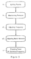
- Figure 3 is a flow diagram of a process utilizing the plasma reactor and match network of figures 1 and 2, respectively.
- the fundamental nonreactive etch prior to metal 2 deposition typically is executed at an etch rate on the order of 250.10 -9 m (250 Angstroms) per minute (equivalent silicon dioxide etch rate) in order to complete this etch step within about 40 seconds. At this rate, this etch step duration plus system overhead to transfer wafers into and out of the reactor meets a system throughput requirement of 60 wafers per hour.
- Many IC circuit designs today contain layers that can be damaged by bombardment by high energy ions. To avoid such damage while retaining an etch time on the order of 40 seconds, the plasma is generated by an rf field of frequency higher than the 13.56 ISM (Industry, Scientific, Medical) frequency that is conventionally utilized.
- the power was adjusted to achieve a 250.10 -9 m (250 Angstroms) per minute equivalent silicon dioxide etch rate
- the negative self bias voltage was measured to be just over 500 volts for a 40 MHZ frequency and was measured to be approximately 310 volts for a 60 MHZ frequency. This confirms that soft etches (i.e., etches with self bias on the order of or less than 500 volts) with acceptable throughput can be produced at these frequencies.
- the self-bias voltage for comparable powers at 137 MHz is -125 volts. Therefore, it appears that a useful range of frequencies for achieving a soft etch that etches the wafer without damaging thin layers extends from 30 MHz to 200 MHz.
- the preferred choice of frequency is in the range 50-70 MHz because this produces the required etch rate under very soft conditions (self-bias near -300 V).
- a frequency f in the range 13.56 MHz ⁇ f ⁇ 200 MHz and an rf power that produces a 250.10 -9 m (250 Angstroms) per minute equivalent silicon dioxide etch rate
- the gas pressure is selected in the range from 0,133 - 2,65 Pa (1 to 20 milliTorr).
- a soft etch process that uses high frequency rf power is useful in both nonreactive, nonselective etch processes and in reactive ion etch processes.
- the power is generally higher and the pressure is generally lower for the nonreactive ion processes.
- the power should be on the order of 300 Watts and the pressure should be on the order of 4 mTorr.
- a reactive ion etch normally employs fluorine-containing or chlorine-containing gases.
- the reactive ion etch containing 10 mole percent NF 3 or 5 mole percent BCl 3 the power should be on the order of 10-50 Watts and the pressure should be on the order of 1,3 - 5,3 Pa (10-40 mTorr.)
- a pair of electromagnetic coils 114 and 115 and associated power supply 116 are included to produce a weak magnetic field that deflects plasma ions away from the walls of the plasma reactor. This is important to avoid contamination of the wafer during processing. Unlike in the prior art, it is not necessary that these fields be uniform at the surface of the wafer because they are too weak (on the order of 10 -4 - 2.10 -3 T (1-20 Gauss) at the surface of the wafer) to significantly affect process uniformity. However, this range of magnetic field is sufficient to prevent plasma ions from impacting the walls with sufficient energy to desorb contaminants from those walls.
- a match network is used to couple power from the 50 ohm impedance rf power line to the much lower impedance plasma without producing a significant amount of reflected power at the match network.
- the conventional match network design cannot be used for the frequencies significantly above 13.56 MHz (i.e., on the order of or greater than 40 MHz).
- cables should be substantially equal to an integral number of quarter wavelengths.
- cable 111 from rf power supply 15 to match network 112 and cable 113 from match network 112 to powered electrode 16 should each be substantially equal to an integral number of quarter wavelengths.
- substantially equal to is meant that this length is equal to an integral number of quarter wavelengths plus or minus 0.05 quarter wavelength. This requirement is easily met at 13.56 MHz where a quarter wavelength is on the order of 4,5 m (15 feet), so a small cutting error of the length of such cable will not be significant.
- a quarter wavelength is about 90 cm (3 feet) so that cable length errors are proportionately 5 times as significant. The addition of a single extra connector or circuit element can violate this cable length criterion.
- the discrete components such as interdigitated blade capacitors and multiple coil inductors, conventionally used in the match network for a 13.56 MHz plasma apparatus are unsuitable for use at the higher frequencies.
- the inductances of such discrete components are too large for frequencies on the order of or greater than 40 MHz.
- an inductor can be a single strip of conductor.
- the multiblade interdigitated blade capacitors of 13.56 MHz systems are replaced by a simple pair of parallel conductive plates spaced by a nonconductor such as a teflon sheet.
- FIG. 2 illustrates a match network design that can be used at frequencies above 40 MHz.
- a ground 20 is connected to the outer conductor of a first rf connector 21 located in a wall 22 of match network 112.
- a conductor 23 electrically connects the inner conductor of connector 21 to a first plate 24 of an input capacitor 27.
- This capacitor also contains a second plate 26 and a dielectric spacer 25.
- Plate 26 is electrically connected to a first plate 28 of a shunt capacitor 211 that also contains a dielectric spacer 29 and a second plate 210.
- Plate 28 is also connected to a first plate 212 of a third capacitor 215, that also includes a dielectric spacer 213 and a second plate 214.
- Plate 214 connects through an inductor 216 to rf electrode 16.
- capacitors 27 and 211 are variable capacitors. In this embodiment, these capacitances are varied by variation of the spacing between plates 24 and 26 and between the spacing between plates 28 and 210. Variation of these spacings is achieved by means of a motor 221 connected by a rotary-to-linear-displacement coupling 222 and a motor 223 connected by a rotary-to-linear-displacement coupling 224. An automated control circuit 225 automatically adjusts these two capacitances to minimize the amount of power reflected at rf coupler 21.
- a detector 226, connected between rf power supply 15 and rf connector 21 provides to control circuit 225 information about the relative phase between the current and voltage components of the rf power input; and the ratio of the magnitudes of the current and voltage components of the rf power input signal.
- Control circuit 225 is a conventional feedback control circuit that adjusts the plate spacings of capacitors 27 and 211 until the relative phase and ratio of magnitudes of the rf current and voltage signals reaches preset values that are selected to produce substantially zero reflection of power back toward the rf power source. Typically, for a tuned match network, this system will produce less than 10 Watts of reflected power from a 300 Watt input signal.
- components 27, 211, 215 and 216 should have the values 10-100 pf, 50-400 pf, 100 pf and 0.5 ⁇ H, respectively.
- variable control of the capacitors enables electrode 16 to function as an igniter electrode to generate a plasma as well as the powered electrode to maintain the plasma.
- the feedback control of capacitors 27 and 211 is inactivated and these capacitances are set respectively to 100 pf and 400 pf. This produces at electrode 16 an electric field strength which is sufficiently large to produce a cascade of electrons that ignites the plasma.
- the self-bias voltage on the powered electrode is on the order of -300 volts for 300 Watts of power at 60 MHz.
- the chosen frequency will not in general be one of the ISM (Industrial, Scientific, Medical) frequencies. Therefore, rf gasketing is used in all vacuum flanges of reactor 10, no windows into chamber 12 are allowed, and all elongated openings in the chamber are eliminated or shielded so that rf radiation from reactor 10 is eliminated to an extent that reduces rf emissions below the United States governmentally allowed level of 15 ⁇ V/m at a distance of 300 m from the apparatus. This avoids interference with TV and other rf communication near such reactors.
- ISM International, Scientific, Medical
Landscapes
- Physics & Mathematics (AREA)
- Engineering & Computer Science (AREA)
- Plasma & Fusion (AREA)
- Chemical & Material Sciences (AREA)
- Analytical Chemistry (AREA)
- Drying Of Semiconductors (AREA)
- ing And Chemical Polishing (AREA)
- Plasma Technology (AREA)
- Chemical Vapour Deposition (AREA)
- Formation Of Insulating Films (AREA)
- Cleaning Or Drying Semiconductors (AREA)
Claims (18)
- Plasmaätzverfahren mit folgenden Schritten:(a) Zünden eines Plasmas in einer Reaktorkammer in einem Plasmareaktor (11) durch eine HF-Spannungsquelle (15) mit einer Frequenz im Bereich von 30 bis 200 MHz;(b) Aufrechterhalten eines Gasdrucks im Bereich von 0,067 - 4 Pa (0,00067 - 0,04 mbar = 0,5 - 30 Millitorr) in der Reaktorkammer; und(c) Zuführen von HF-Spannung zu einer gespeisten Substratstützelektrode (16), worauf ein Wafer (17) zur Verarbeitung positioniert wird, wobei der Spannungspegel P eingestellt wird, um das Plasma in der Reaktorkammer aufrechtzuerhalten, und um eine negative automatische Spannung (negative self-bias voltage) an der gespeisten Elektrode von weniger als 350 Volt zu erzeugen, um einen Weichplasmaätzprozeß zu schaffen.
- Verfahren gemäß Anspruch 1, bei dem die Spannung P und die Frequenz f ausgewählt sind, um eine negative automatische Spannung (negative self-bias) an der gespeisten Elektrode von mehr als 150 Volt für einen nichtreaktiven Weichätzprozeß zu erzeugen.
- Verfahren gemäß einem der Ansprüche 1 und 2, bei dem die Spannung P und die Frequenz f ausgewählt sind, um eine negative automatische Spannung (negative self-bias) an der gespeisten Elektrode von mehr als 50 Volt für einen weichen reaktiven Ionenätzprozeß zu erzeugen.
- Verfahren gemäß Ansprüchen 1 bis 3, bei dem die Frequenz f im Bereich von 50 - 70 MHz liegt, wodurch dieses Verfahren insbesondere für einen Weichplasmaätzprozeß geeignet ist.
- Verfahren gemäß einem der Ansprüche 1 bis 4, bei dem in Schritt (a) HF-Spannung der gespeisten Elektrode (16) durch ein Anpassungsnetzwerk (112) zugeführt wird, welches verstimmt wird, um ein ausreichend starkes Feld der automatischen Spannung (self-bias) an der gespeisten Elektrode (16) zu erzeugen, daß eine Elektronenlawine erzeugt wird, wodurch das Plasma gezündet wird, wobei das Verfahren des weiteren den Schritt (a1) des Stimmens des Anpassungsnetzwerks (112) umfaßt, um reflektierte Leistung im wesentlichen zu eliminieren.
- Verfahren gemäß einem der vorhergehenden Ansprüche, das des weiteren folgenden Schritt umfaßt:(a1) Einstellung eines Anpassungsnetzwerks (112), so daß es bei einer ausgewählten Frequenz f zur Verwendung während des Ätzens eines Wafers (17) im wesentlichen keine Reflexion von Leistung zurück zu einer Quelle der HF-Spannung gibt.
- Verfahren gemäß einem der Ansprüche 1 bis 3, bei dem die Frequenz f 40,68 MHz beträgt, wodurch Strahlungsspannungspegeleinschränkungen weniger einschränkend sind als bei Nicht-ISM-Frequenzen.
- Verfahren gemäß einem der vorhergehenden Ansprüche, bei dem das Plasma in einem Gas ausgewählt aus der Gruppe bestehend aus reinem Argon, reinem Wasserstoff, Gasmischungen mit fluorhaltigen Gasen und Gasmischungen mit chlorhaltigen Gasen erzeugt wird.
- Plasmaätzvorrichtung mit:einem Plasmareaktor (11) mit einer gespeisten Stützelektrode (16), worauf ein Wafer (17) während der Verarbeitung positioniert ist; undeiner HF-Spannungsquelle (15), die eine Spannung P mit einem Pegel erzeugt, welcher ausreicht, das Plasma in dem Reaktor bei einer Frequenz f im Bereich von 30 bis 200 MHz aufrechtzuerhalten, wobei die Spannung P und die Frequenz f ausgewählt sind, um eine negative automatische Spannung (negative self-bias) an der gespeisten Elektrode von weniger als 350 Volt zu erzeugen.
- Plasmaätzvorrichtung gemäß Anspruch 9, bei dem die Spannung P und die Frequenz f ausgewählt sind, um eine negative automatische Spannung (negative self-bias) an der gespeisten Elektrode von mehr als 150 Volt für einen nichtreaktiven Weichätzprozeß zu erzeugen.
- Plasmaätzvorrichtung gemäß einem der Ansprüche 9 und 10, bei dem die Spannung P und die Frequenz f ausgewählt sind, um eine negative automatische Spannung (negative self-bias) an der gespeisten Elektrode von mehr als 50 Volt für einen weichen reaktiven Ionenätzprozeß zu erzeugen.
- Plasmaätzvorrichtung gemäß einem der Ansprüche 9 bis 11, weiterhin mit einem Anpassungsnetzwerk (112) an einem HF-Spannungseingang zur gespeisten Elektrode, wobei das Anpassungsnetzwerk Reflexionen eines HF-Signals bei Frequenzen im Bereich von 30 bis 200 MHz im wesentlichen eliminieren kann.
- Plasmaätzvorrichtung gemäß den Ansprüchen 9 bis 12, bei der das Anpassungsnetzwerk (112) über einen Frequenzbereich stimmbar ist, wodurch eine Frequenzeinstellung möglich ist, um Plasmaprozeßbedingungen zu optimieren.
- Plasmaätzvorrichtung gemäß einem der Ansprüche 9 bis 13, bei der der Reaktor HF-abgeschirmt ist.
- Plasmaätzvorrichtung gemäß Anspruch 14, bei der die Frequenz im Bereich von 50 - 70 MHz liegt, wodurch diese Vorrichtung insbesondere für den Plasmaätzprozeß geeignet ist.
- Plasmaätzvorrichtung gemäß einem der Ansprüche 9 bis 14, bei der die Frequenz die ISM-Standardfrequenz von 40,68 MHz ist.
- Plasmaätzvorrichtung gemäß einem der Ansprüche 9 bis 16, weiterhin mit Mitteln (114, 115) zur Erzeugung eines Magnetfeldes parallel zur Wand des Reaktors in der Vorrichtung, welches ausreichend schwach ist, daß es die Prozeßrate oder -gleichmäßigkeit nicht erheblich beeinflußt, und das ausreichend stark ist, daß es Ionen von den Wänden ablenkt.
- Plasmaätzvorrichtung gemäß Anspruch 17, bei der das Magnetfeld an den Innenwänden im Bereich von 0,0001 - 0,002 Tesla (1 - 20 Gauss) liegt.
Applications Claiming Priority (2)
| Application Number | Priority Date | Filing Date | Title |
|---|---|---|---|
| US41675089A | 1989-10-03 | 1989-10-03 | |
| US416750 | 1989-10-03 |
Publications (4)
| Publication Number | Publication Date |
|---|---|
| EP0421430A2 EP0421430A2 (de) | 1991-04-10 |
| EP0421430A3 EP0421430A3 (en) | 1991-08-14 |
| EP0421430B1 true EP0421430B1 (de) | 1997-04-02 |
| EP0421430B2 EP0421430B2 (de) | 2003-12-10 |
Family
ID=23651158
Family Applications (1)
| Application Number | Title | Priority Date | Filing Date |
|---|---|---|---|
| EP90119065A Expired - Lifetime EP0421430B2 (de) | 1989-10-03 | 1990-10-04 | Plasmaprozess, Verfahren und Gerät |
Country Status (5)
| Country | Link |
|---|---|
| EP (1) | EP0421430B2 (de) |
| JP (2) | JP2634313B2 (de) |
| KR (1) | KR0170387B1 (de) |
| DE (1) | DE69030347T2 (de) |
| ES (1) | ES2100859T3 (de) |
Families Citing this family (20)
| Publication number | Priority date | Publication date | Assignee | Title |
|---|---|---|---|---|
| US5312778A (en) * | 1989-10-03 | 1994-05-17 | Applied Materials, Inc. | Method for plasma processing using magnetically enhanced plasma chemical vapor deposition |
| WO1993021685A1 (en) * | 1992-04-16 | 1993-10-28 | Advanced Energy Industries, Inc. | Stabilizer for switch-mode powered rf plasma processing |
| US6835523B1 (en) | 1993-05-09 | 2004-12-28 | Semiconductor Energy Laboratory Co., Ltd. | Apparatus for fabricating coating and method of fabricating the coating |
| US6238533B1 (en) * | 1995-08-07 | 2001-05-29 | Applied Materials, Inc. | Integrated PVD system for aluminum hole filling using ionized metal adhesion layer |
| US5962923A (en) * | 1995-08-07 | 1999-10-05 | Applied Materials, Inc. | Semiconductor device having a low thermal budget metal filling and planarization of contacts, vias and trenches |
| US6902683B1 (en) | 1996-03-01 | 2005-06-07 | Hitachi, Ltd. | Plasma processing apparatus and plasma processing method |
| US6252354B1 (en) * | 1996-11-04 | 2001-06-26 | Applied Materials, Inc. | RF tuning method for an RF plasma reactor using frequency servoing and power, voltage, current or DI/DT control |
| TW335517B (en) * | 1996-03-01 | 1998-07-01 | Hitachi Ltd | Apparatus and method for processing plasma |
| WO1999027579A1 (en) | 1997-11-26 | 1999-06-03 | Applied Materials, Inc. | Damage-free sculptured coating deposition |
| US7253109B2 (en) | 1997-11-26 | 2007-08-07 | Applied Materials, Inc. | Method of depositing a tantalum nitride/tantalum diffusion barrier layer system |
| KR100521120B1 (ko) * | 1998-02-13 | 2005-10-12 | 가부시끼가이샤 히다치 세이사꾸쇼 | 반도체소자의 표면처리방법 및 장치 |
| US6143144A (en) * | 1999-07-30 | 2000-11-07 | Tokyo Electronlimited | Method for etch rate enhancement by background oxygen control in a soft etch system |
| JP4666740B2 (ja) * | 2000-10-06 | 2011-04-06 | 川崎マイクロエレクトロニクス株式会社 | 半導体製造装置、被処理基板表面の処理方法およびプラズマ生成物の付着状態の観察方法 |
| US20030077910A1 (en) * | 2001-10-22 | 2003-04-24 | Russell Westerman | Etching of thin damage sensitive layers using high frequency pulsed plasma |
| DE10318566B4 (de) * | 2003-04-15 | 2005-11-17 | Fresnel Optics Gmbh | Verfahren und Werkzeug zur Herstellung transparenter optischer Elemente aus polymeren Werkstoffen |
| KR101151414B1 (ko) * | 2010-02-23 | 2012-06-04 | 주식회사 플라즈마트 | 임피던스 정합 장치 |
| US8576013B2 (en) * | 2011-12-29 | 2013-11-05 | Mks Instruments, Inc. | Power distortion-based servo control systems for frequency tuning RF power sources |
| CN103456591B (zh) * | 2012-05-31 | 2016-04-06 | 中微半导体设备(上海)有限公司 | 自动频率调谐源和偏置射频电源的电感耦合等离子处理室 |
| KR101657915B1 (ko) * | 2012-08-31 | 2016-09-19 | 에바텍 어드벤스드 테크놀로지스 아크티엔게젤샤프트 | 질화 알루미늄층의 증착 방법 |
| US10347464B2 (en) * | 2015-09-15 | 2019-07-09 | Lam Research Corporation | Cycle-averaged frequency tuning for low power voltage mode operation |
Family Cites Families (13)
| Publication number | Priority date | Publication date | Assignee | Title |
|---|---|---|---|---|
| US4375051A (en) * | 1981-02-19 | 1983-02-22 | The Perkin-Elmer Corporation | Automatic impedance matching between source and load |
| US4585668A (en) * | 1983-02-28 | 1986-04-29 | Michigan State University | Method for treating a surface with a microwave or UHF plasma and improved apparatus |
| JPS6094725A (ja) * | 1983-10-28 | 1985-05-27 | Hitachi Ltd | ドライエツチング装置 |
| US4572759A (en) * | 1984-12-26 | 1986-02-25 | Benzing Technology, Inc. | Troide plasma reactor with magnetic enhancement |
| JPS62125626A (ja) * | 1985-11-27 | 1987-06-06 | Hitachi Ltd | ドライエツチング装置 |
| JPH0831438B2 (ja) † | 1986-02-19 | 1996-03-27 | 株式会社日立製作所 | マイクロ波プラズマ処理装置 |
| JPS62280379A (ja) † | 1986-05-30 | 1987-12-05 | Hitachi Ltd | エツチング装置 |
| CH668145A5 (fr) * | 1986-09-26 | 1988-11-30 | Inst Microtechnique De L Unive | Procede et installation de depot de silicium amorphe hydrogene sur un substrat dans une enceinte a plasma. |
| EP0277460A1 (de) * | 1986-12-16 | 1988-08-10 | Plasma-Seven S.A. | Verfahren zur Wiedergabe der metallischen Struktur in einer degradierten Oberfläche eines metallischen Objekts, Anwendung und Vorrichtung zur Ausarbeitung dieses Verfahrens |
| JPS63279609A (ja) * | 1987-05-11 | 1988-11-16 | Shindengen Electric Mfg Co Ltd | Rf発生装置の自動整合装置 |
| US5079031A (en) † | 1988-03-22 | 1992-01-07 | Semiconductor Energy Laboratory Co., Ltd. | Apparatus and method for forming thin films |
| JPH024238U (de) * | 1988-06-20 | 1990-01-11 | ||
| JPH02298024A (ja) * | 1989-05-12 | 1990-12-10 | Tadahiro Omi | リアクティブイオンエッチング装置 |
-
1990
- 1990-09-29 KR KR1019900015671A patent/KR0170387B1/ko not_active Expired - Lifetime
- 1990-10-01 JP JP2263689A patent/JP2634313B2/ja not_active Expired - Fee Related
- 1990-10-04 DE DE69030347T patent/DE69030347T2/de not_active Expired - Fee Related
- 1990-10-04 ES ES90119065T patent/ES2100859T3/es not_active Expired - Lifetime
- 1990-10-04 EP EP90119065A patent/EP0421430B2/de not_active Expired - Lifetime
-
1996
- 1996-05-30 JP JP13695196A patent/JP3236216B2/ja not_active Expired - Fee Related
Also Published As
| Publication number | Publication date |
|---|---|
| DE69030347D1 (de) | 1997-05-07 |
| JPH09232292A (ja) | 1997-09-05 |
| KR0170387B1 (ko) | 1999-03-30 |
| EP0421430B2 (de) | 2003-12-10 |
| KR910008796A (ko) | 1991-05-31 |
| JPH03171623A (ja) | 1991-07-25 |
| JP3236216B2 (ja) | 2001-12-10 |
| EP0421430A2 (de) | 1991-04-10 |
| EP0421430A3 (en) | 1991-08-14 |
| ES2100859T3 (es) | 1997-07-01 |
| DE69030347T2 (de) | 1997-07-17 |
| JP2634313B2 (ja) | 1997-07-23 |
Similar Documents
| Publication | Publication Date | Title |
|---|---|---|
| US5223457A (en) | High-frequency semiconductor wafer processing method using a negative self-bias | |
| US5849136A (en) | High frequency semiconductor wafer processing apparatus and method | |
| EP0421430B1 (de) | Plasmaprozess, Verfahren und Gerät | |
| US5534231A (en) | Low frequency inductive RF plasma reactor | |
| US9053908B2 (en) | Method and apparatus for controlling substrate DC-bias and ion energy and angular distribution during substrate etching | |
| US6143129A (en) | Inductive plasma reactor | |
| JP3653524B2 (ja) | プラズマ発生方法、および誘導結合されたプラズマ発生源を含むプラズマ発生装置 | |
| US6777037B2 (en) | Plasma processing method and apparatus | |
| US20020187280A1 (en) | Method and system for reducing damage to substrates during plasma processing with a resonator source | |
| JPH0684811A (ja) | プラズマ発生装置 | |
| JP3319285B2 (ja) | プラズマ処理装置及びプラズマ処理方法 | |
| US6939813B2 (en) | Apparatus for improved low pressure inductively coupled high density plasma reactor | |
| KR101191698B1 (ko) | 저압력 플라즈마를 점화시키는 방법 및 장치 | |
| Lieberman et al. | Plasma generation for materials processing | |
| JPH09260352A (ja) | プラズマ処理装置及びプラズマ処理方法 | |
| KR100420533B1 (ko) | 플라즈마 공정장치 및 이를 이용한 플라즈마 식각방법 |
Legal Events
| Date | Code | Title | Description |
|---|---|---|---|
| PUAI | Public reference made under article 153(3) epc to a published international application that has entered the european phase |
Free format text: ORIGINAL CODE: 0009012 |
|
| AK | Designated contracting states |
Kind code of ref document: A2 Designated state(s): BE DE ES FR GB IT NL |
|
| PUAL | Search report despatched |
Free format text: ORIGINAL CODE: 0009013 |
|
| AK | Designated contracting states |
Kind code of ref document: A3 Designated state(s): BE DE ES FR GB IT NL |
|
| 17P | Request for examination filed |
Effective date: 19920114 |
|
| 17Q | First examination report despatched |
Effective date: 19940126 |
|
| GRAH | Despatch of communication of intention to grant a patent |
Free format text: ORIGINAL CODE: EPIDOS IGRA |
|
| ITF | It: translation for a ep patent filed | ||
| GRAH | Despatch of communication of intention to grant a patent |
Free format text: ORIGINAL CODE: EPIDOS IGRA |
|
| GRAA | (expected) grant |
Free format text: ORIGINAL CODE: 0009210 |
|
| AK | Designated contracting states |
Kind code of ref document: B1 Designated state(s): BE DE ES FR GB IT NL |
|
| PG25 | Lapsed in a contracting state [announced via postgrant information from national office to epo] |
Ref country code: FR Free format text: LAPSE BECAUSE OF NON-PAYMENT OF DUE FEES Effective date: 19970402 Ref country code: NL Free format text: LAPSE BECAUSE OF FAILURE TO SUBMIT A TRANSLATION OF THE DESCRIPTION OR TO PAY THE FEE WITHIN THE PRESCRIBED TIME-LIMIT Effective date: 19970402 |
|
| REF | Corresponds to: |
Ref document number: 69030347 Country of ref document: DE Date of ref document: 19970507 |
|
| ET | Fr: translation filed | ||
| REG | Reference to a national code |
Ref country code: ES Ref legal event code: FG2A Ref document number: 2100859 Country of ref document: ES Kind code of ref document: T3 |
|
| PLBQ | Unpublished change to opponent data |
Free format text: ORIGINAL CODE: EPIDOS OPPO |
|
| PLBI | Opposition filed |
Free format text: ORIGINAL CODE: 0009260 |
|
| PLBF | Reply of patent proprietor to notice(s) of opposition |
Free format text: ORIGINAL CODE: EPIDOS OBSO |
|
| 26 | Opposition filed |
Opponent name: INSTITUTE OF TECHNOLOGICAL INFORMATION, INC. Effective date: 19980102 |
|
| NLR1 | Nl: opposition has been filed with the epo |
Opponent name: INSTITUTE OF TECHNOLOGICAL INFORMATION, INC. |
|
| PLBF | Reply of patent proprietor to notice(s) of opposition |
Free format text: ORIGINAL CODE: EPIDOS OBSO |
|
| PLAW | Interlocutory decision in opposition |
Free format text: ORIGINAL CODE: EPIDOS IDOP |
|
| APAC | Appeal dossier modified |
Free format text: ORIGINAL CODE: EPIDOS NOAPO |
|
| APAE | Appeal reference modified |
Free format text: ORIGINAL CODE: EPIDOS REFNO |
|
| APAC | Appeal dossier modified |
Free format text: ORIGINAL CODE: EPIDOS NOAPO |
|
| APAE | Appeal reference modified |
Free format text: ORIGINAL CODE: EPIDOS REFNO |
|
| PGFP | Annual fee paid to national office [announced via postgrant information from national office to epo] |
Ref country code: DE Payment date: 20011029 Year of fee payment: 12 |
|
| REG | Reference to a national code |
Ref country code: GB Ref legal event code: IF02 |
|
| PGFP | Annual fee paid to national office [announced via postgrant information from national office to epo] |
Ref country code: FR Payment date: 20021008 Year of fee payment: 13 |
|
| PGFP | Annual fee paid to national office [announced via postgrant information from national office to epo] |
Ref country code: NL Payment date: 20021031 Year of fee payment: 13 Ref country code: ES Payment date: 20021031 Year of fee payment: 13 |
|
| PGFP | Annual fee paid to national office [announced via postgrant information from national office to epo] |
Ref country code: BE Payment date: 20021219 Year of fee payment: 13 |
|
| APAC | Appeal dossier modified |
Free format text: ORIGINAL CODE: EPIDOS NOAPO |
|
| PLAW | Interlocutory decision in opposition |
Free format text: ORIGINAL CODE: EPIDOS IDOP |
|
| PG25 | Lapsed in a contracting state [announced via postgrant information from national office to epo] |
Ref country code: DE Free format text: LAPSE BECAUSE OF NON-PAYMENT OF DUE FEES Effective date: 20030501 |
|
| PUAH | Patent maintained in amended form |
Free format text: ORIGINAL CODE: 0009272 |
|
| STAA | Information on the status of an ep patent application or granted ep patent |
Free format text: STATUS: PATENT MAINTAINED AS AMENDED |
|
| PG25 | Lapsed in a contracting state [announced via postgrant information from national office to epo] |
Ref country code: BE Free format text: LAPSE BECAUSE OF NON-PAYMENT OF DUE FEES Effective date: 20031031 |
|
| 27A | Patent maintained in amended form |
Effective date: 20031210 |
|
| AK | Designated contracting states |
Kind code of ref document: B2 Designated state(s): BE DE ES FR GB IT NL |
|
| NLR2 | Nl: decision of opposition |
Effective date: 20031210 |
|
| PG25 | Lapsed in a contracting state [announced via postgrant information from national office to epo] |
Ref country code: ES Free format text: LAPSE BECAUSE OF FAILURE TO SUBMIT A TRANSLATION OF THE DESCRIPTION OR TO PAY THE FEE WITHIN THE PRESCRIBED TIME-LIMIT Effective date: 20040321 |
|
| NLV1 | Nl: lapsed or annulled due to failure to fulfill the requirements of art. 29p and 29m of the patents act | ||
| REG | Reference to a national code |
Ref country code: FR Ref legal event code: ST |
|
| EN | Fr: translation not filed | ||
| PG25 | Lapsed in a contracting state [announced via postgrant information from national office to epo] |
Ref country code: IT Free format text: LAPSE BECAUSE OF NON-PAYMENT OF DUE FEES;WARNING: LAPSES OF ITALIAN PATENTS WITH EFFECTIVE DATE BEFORE 2007 MAY HAVE OCCURRED AT ANY TIME BEFORE 2007. THE CORRECT EFFECTIVE DATE MAY BE DIFFERENT FROM THE ONE RECORDED. Effective date: 20051004 |
|
| APAH | Appeal reference modified |
Free format text: ORIGINAL CODE: EPIDOSCREFNO |
|
| PGFP | Annual fee paid to national office [announced via postgrant information from national office to epo] |
Ref country code: GB Payment date: 20080915 Year of fee payment: 19 |
|
| PG25 | Lapsed in a contracting state [announced via postgrant information from national office to epo] |
Ref country code: GB Free format text: LAPSE BECAUSE OF NON-PAYMENT OF DUE FEES Effective date: 20091004 |