EP0421433B1 - Circuit de traitement de signaux pour dispositif de prise d'images à l'état solide - Google Patents
Circuit de traitement de signaux pour dispositif de prise d'images à l'état solide Download PDFInfo
- Publication number
- EP0421433B1 EP0421433B1 EP90119070A EP90119070A EP0421433B1 EP 0421433 B1 EP0421433 B1 EP 0421433B1 EP 90119070 A EP90119070 A EP 90119070A EP 90119070 A EP90119070 A EP 90119070A EP 0421433 B1 EP0421433 B1 EP 0421433B1
- Authority
- EP
- European Patent Office
- Prior art keywords
- signal
- data
- output
- circuit
- color
- Prior art date
- Legal status (The legal status is an assumption and is not a legal conclusion. Google has not performed a legal analysis and makes no representation as to the accuracy of the status listed.)
- Expired - Lifetime
Links
Images






Classifications
-
- H—ELECTRICITY
- H04—ELECTRIC COMMUNICATION TECHNIQUE
- H04N—PICTORIAL COMMUNICATION, e.g. TELEVISION
- H04N23/00—Cameras or camera modules comprising electronic image sensors; Control thereof
- H04N23/80—Camera processing pipelines; Components thereof
- H04N23/82—Camera processing pipelines; Components thereof for controlling camera response irrespective of the scene brightness, e.g. gamma correction
- H04N23/83—Camera processing pipelines; Components thereof for controlling camera response irrespective of the scene brightness, e.g. gamma correction specially adapted for colour signals
-
- H—ELECTRICITY
- H04—ELECTRIC COMMUNICATION TECHNIQUE
- H04N—PICTORIAL COMMUNICATION, e.g. TELEVISION
- H04N9/00—Details of colour television systems
- H04N9/64—Circuits for processing colour signals
- H04N9/646—Circuits for processing colour signals for image enhancement, e.g. vertical detail restoration, cross-colour elimination, contour correction, chrominance trapping filters
-
- H—ELECTRICITY
- H03—ELECTRONIC CIRCUITRY
- H03M—CODING; DECODING; CODE CONVERSION IN GENERAL
- H03M1/00—Analogue/digital conversion; Digital/analogue conversion
- H03M1/12—Analogue/digital converters
-
- H—ELECTRICITY
- H04—ELECTRIC COMMUNICATION TECHNIQUE
- H04N—PICTORIAL COMMUNICATION, e.g. TELEVISION
- H04N23/00—Cameras or camera modules comprising electronic image sensors; Control thereof
- H04N23/10—Cameras or camera modules comprising electronic image sensors; Control thereof for generating image signals from different wavelengths
- H04N23/13—Cameras or camera modules comprising electronic image sensors; Control thereof for generating image signals from different wavelengths with multiple sensors
-
- H—ELECTRICITY
- H04—ELECTRIC COMMUNICATION TECHNIQUE
- H04N—PICTORIAL COMMUNICATION, e.g. TELEVISION
- H04N23/00—Cameras or camera modules comprising electronic image sensors; Control thereof
- H04N23/80—Camera processing pipelines; Components thereof
- H04N23/84—Camera processing pipelines; Components thereof for processing colour signals
- H04N23/843—Demosaicing, e.g. interpolating colour pixel values
-
- H—ELECTRICITY
- H04—ELECTRIC COMMUNICATION TECHNIQUE
- H04N—PICTORIAL COMMUNICATION, e.g. TELEVISION
- H04N25/00—Circuitry of solid-state image sensors [SSIS]; Control thereof
- H04N25/10—Circuitry of solid-state image sensors [SSIS]; Control thereof for transforming different wavelengths into image signals
- H04N25/11—Arrangement of colour filter arrays [CFA]; Filter mosaics
-
- H—ELECTRICITY
- H04—ELECTRIC COMMUNICATION TECHNIQUE
- H04N—PICTORIAL COMMUNICATION, e.g. TELEVISION
- H04N25/00—Circuitry of solid-state image sensors [SSIS]; Control thereof
- H04N25/60—Noise processing, e.g. detecting, correcting, reducing or removing noise
- H04N25/62—Detection or reduction of noise due to excess charges produced by the exposure, e.g. smear, blooming, ghost image, crosstalk or leakage between pixels
Definitions
- This invention relates to an apparatus in which the imaging section is arranged with a spatial pixel shifting or offsetting in which the solid state image sensors for green and red color imaging are arranged with a spatial offset of one half the pixel repetition pitch in accordance with the precharacterizing part of claim 1.
- Such an image processing apparatus is known from EP-A-0 368 354 which represents prior art according to Article 54(3) EPC.
- the imaging section is constituted by a solid-state image sensor having a discrete pixel structure formed by charge coupled devices (CCDs)
- CCDs charge coupled devices
- the conventional practice for preventing aliasing components from being mixed into the baseband of the imaging signals is to suppress the high frequency side of the baseband components of the imaging signal to satisfy the Nyquist conditions of the sampling system by the solid state image sensor.
- a multi-CCD type solid-state imaging apparatus such as a two CCD type imaging apparatus in which a three-color image is formed by a solid-state image sensor provided with a solid-state image sensor for forming a green color image and a color coding filter for each of the red and blue pixels, or a three CCD type solid-state image forming apparatus in which the three-color image is formed by separate solid-state image sensors, are put to practical use.
- EP-A-0 368 354 representing prior art according to Article 54(3) EPC and corresponding to the precharacterizing part of claim 1 describes a signal-processing circuit including an image enhancement section which comprises in series connection a first and a second lH-delay circuit and an image enhancement data forming circuit.
- the image enhancement data forming circuit is directly supplied with green color data from the A/D converter for the green color image signal. Further, the image enhancement data forming circuit is supplied with one lH-delayed green color data and 2H-delayed green color data and further with non-delayed red color data from the A/D converter for the red color image signal. On the basis of these delayed and non-delayed signals the image enhancement data forming circuit forms image enhancement data having a clock rate 2 fs twice the clock-rate fs. This image enhancement data is supplied to first adders and to second adders, respectively provided in the signal path of the interpolated green color data, red color data, blue color data before and after gamma-correction circuits, respectively.
- the first adders provided upstream of the gamma-correction circuits sum the image enhancement data with the clock rate of 2 fs to the interpolated color data having the clock rate 2 fs and transmit the image enhancement color data to the corresponding gamma correction circuit.
- the gamma correction circuits perform gamma correction of the enhanced color data from the first adders and transmit the gamma-corrected color data to the second adders downstream of the gamma-correction circuits.
- the second adders are summing the image enhancement data supplied from the image enhancement section at the clock rate of 2 fs to the gamma-corrected color data from the gamma-correction circuit.
- the gamma-corrected and enhanced color data having the clock rate 2 fs are respectively transmitted to a color encoder and digital/analog converters converting the high resolution color data supplied with the clock rate 2 fs into analog three-color image pick-up output signals.
- said signal processing circuit is adapted to eliminate aliasing components contained in the detail signal and to prevent the cross-color interference from being generated as a result of the mixing of the horizontal detail signals into the color subcarrier frequency region.
- gamma compensation or image enhancement may be performed satisfactorily without picture quality deterioration due to the aliasing components or cross-color interference.
- output imaging signals read from the solid-state image sensor at the sampling rate equal to fs are subjected to image enhancement at the clock rate equal to 2 fs.
- said digital output signals processed by image enhancement at the clock rate equal to 2 fs may be satisfactorily processed by gamma correction.
- It is a further embodiment of the present signal processing circuit to employ digital filters for interpolation and for producing the detail signal which are selected to have zero points at the frequency equal to fs and to have the same number of orders as to odd and even order numbers.
- the present signal processing circuit is adapted to provide optimum image enhancement coping with changes in the imaging environment.
- the detail signal formed from the output imaging signal produced at the imaging section may be subjected to a non-linear arithmetic operation in which compression characteristics on the more positive and more negative level side with respect to a predetermined level may be set independently.
- the input signal may be clipped at a predetermined level by a non-linear arithmetic operation.
- the preferred signal processing circuit is adapted to produce the broad range detail signal free from aliasing components for the output imaging signal.
- a signal-processing circuit for a solid-state imaging apparatus in which the vertical detail signal is band-limited in the horizontal direction before being outputted to prevent the vertical detail signal component from being mixed into the region of the color subcarrier frequency.
- Fig. 1 is a diagrammatic view showing the signal spectrum of an output imaging signal by a customary solid-state image sensor having a discrete pixel arrangement.
- Fig. 2 is a block diagram showing a three CCD type color television camera to which the present invention is applied.
- Fig. 3 is a diagrammatic view showing the arraying state of the CCD image sensors in the color television camera shown in Fig. 2.
- Fig. 4 shows the signal spectrum for each output imaging signal from the associated CCD image sensor of the color television camera shown in Fig. 2.
- Fig. 5 is a block diagram showing the arrangement of a signal processing section of the color television camera shown in Fig. 2.
- Fig. 6 is a block diagram showing another embodiment of the signal processing section of the color television camera shown in Fig. 2.
- Fig. 7 is a chart showing filtering characteristics of a digital filter provided in an interpolator of the signal processing section.
- Fig. 8 is a chart showing filtering characteristics of a digital filter provided in a detail signal generator of the signal processing section.
- Fig. 9 is a chart for illustrating the horizontal contour enhancement for the case in which the even number order interpolation is performed in the interpolating section and the odd number order interpolation is performed in the detail signal generator.
- Fig. 10 is a chart for illustrating the horizontal contour enhancement operation for the case in which the even number order interpolation is performed in interpolator and the even number order differentiating operation is performed in the detail signal generator.
- Fig. 11 is a chart for illustrating the horizontal contour enhancement operation for the case in which the even number order interpolation is performed in the interpolator and the odd number order differentiating operation is performed in the detail signal generator.
- Fig. 12 is a block diagram showing a concrete example of the construction of the detail signal generator of the signal processing section.
- Fig. 13 is a block diagram showing an equivalent block construction of a first digital filter circuit of the detail signal generator.
- Fig. 14 is a chart showing filtering characteristics of the first digital filter circuit.
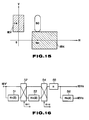
- Fig. 15 is a diagrammatic view showing frequency characteristics of the detail signal formed in the detail signal generator.
- Fig. 16 is a block diagram showing an equivalent block construction of a second digital filter circuit of the digital signal generator.
- Fig. 17 is a chart showing filtering characteristics of the second digital filter circuit.
- Fig. 18 is a block diagram showing another equivalent block construction of the second digital filter circuit of the detail signal generator.
- Figs. 19A, 19B and 19C are block diagrams showing concrete constructions of first to third filter blocks in the second digital filter circuit shown in Fig. 18.
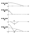
- Figs. 20A, 20B, 20C and 20D are charts for illustrating the band-limiting operation of the second digital filter circuit shown in Fig. 18.
- Fig. 21 is a block diagram showing a concrete block construction of a second core circuit of the detail signal generator shown in Fig. 12.
- Fig. 22 is a chart showing characteristics of a non-linear operation of the second core circuit shown in Fig. 21.
- Fig. 23 is a block diagram showing another block construction of the second core circuit of the detail signal generator shown in Fig. 12.
- Fig. 24 is a chart showing characteristics of the non-linear operation of the second core circuit shown in Fig. 23.
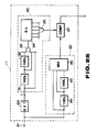
- Fig. 25 is a block diagram showing another embodiment of the detail signal generator of the signal processing section of the color television camera shown in Fig. 2.
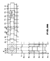
- Fig. 26 is a waveform diagram for illustrating the contour compensating operation of the detail signal generator shown in Fig. 25.
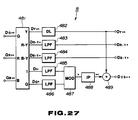
- Fig. 27 is a block diagram showing the construction of a color encoder of the color television camera shown in Fig. 2.
- Fig. 2 shows a color television camera in which the present invention is applied to a three CCD solid-state imaging apparatus in which an imaging light L i incident from an imaging lens 1 by way of an optical low-pass filter 2 is separated by a color separating filter 3 into three prime color light components, that is a red (R), green (G) and blue (B) color light components, for imaging the three-color images of an object image on three CCD image sensors 4R, 4G and 4B.
- R red
- G green
- B blue
- the three CCD image sensors 4R, 4G and 4B constituting the imaging section of the color television camera are arrayed under the principle of spatial pixel offsetting so that the CCD image sensor 4R for forming the red color image and the CCD image sensor 4B for forming the blue color image are offset by one half the spatial sampling period ⁇ s with respect to the CCD image sensor 4G for forming the green color image.
- the three CCD image sensors 4R, 4G and 4B are driven by CCD driving circuits, not shown, so that the imaging charges of the pixels are read out by read-out clocks having a sampling frequency fs equal to four times the color sub-carrier frequency fsc, or 4 fsc.
- the CCD image sensor 4G for green color image on one hand and the CCD image sensors 4R and 4B for forming the red and blue color images on the other perform spatial sampling of the three color object images at positions offset by ⁇ s/2 from each other.
- the imaging output signals S R* , S G* and S B* are read out from the CCD image sensors 4R, 4G and 4B in such a manner that the sampling frequency component fs of the green imaging output signal S G* by the CCD image sensor 4G is antiphase with respect to the sampling frequency components fs of the red color image output signal S R* and the blue color image output signal S B* by the CCD image sensors 4R and 4B, as shown in Fig. 4 showing signal spectral components.
- the imaging output signals S R* , S G* and S B* , read out from the CCD image sensors 4R, 4G and 4B by read-out clocks of the sampling frequency fs or 4 fsc, are supplied to analog/digital converters (A/D converters) 6R, 6G and 6B, respectively, by means of buffer amplifiers 5R, 5G and 5B.
- A/D converters analog/digital converters
- A/D converters 6R, 6G and 6B are supplied clocks having a clock rate fs equal to the sampling rate of the image output signals S R* , S G* and S B* , that is a clock frequency fs or 4 fsc equal to the read-out clocks of the CCD image sensors 4R, 4G and 4B.
- the A/D converters 6R, 6G and 6B directly digitize the imaging output signals S R* , S G* and S B* at the clock rate fs or 4 fsc to form color data D R* , D G* and D B* having the output spectrum that is the same as the spectrum of the imaging output signal S R* , S G* and S B* shown in Fig. 4.
- the color data D R* , D G* and D B* , produced by the A/D converters 6R, 6G and 6B, are transmitted to a signal processor 7.
- the signal processor 7 is constituted, as shown in Fig. 5 showing its concrete construction, by a detail signal generator 11 supplied with red color data D R* from the A/D converter 6R and green color data D G* from the A/D converter 6G, interpolators 13R, 13G and 13B supplied with three color data D R* , D G* and D B* from the A/D converters 6R, 6G and 6B via delay circuits 12R, 12G and 12B, summing points or circuits 14R, 14G and 14B supplied with previously interpolated three color data D R** , D G** and D B* from the interpolators 13R, 13G and 13B and with detail signal D IE** from detail signal generator 11, and gamma correction circuits 15R, 15G and 15B supplied with a summation output from the summation points 14R, 14G and 14B.
- the interpolators 13R, 13G and 13B of the signal processor 7 interpolate the three color data D R* , D G* and D B* of the clock rate fs equal to 4 fsc from the A/D converters 6R, 6G and 6B to form the three color data D R** D G** and D B** of the clock rate 2 fs equal to 8 fsc which is twice the clock rate fs.
- the interpolators 13R, 13G and 13B transmit the three color data D R** , D G** and D B** of the clock rate equal to 2 fs to the summing points 14R, 14G and 14B.
- the detail signal generator 11 is constituted by summing means for summing equal amounts of green color data D G* of the fs rate from the A/D converter 6G and red color data D R* of the fs rate from the A/D converter 6R after multiplexing at the clock rate 2 fs and a digital filter for differentiating an addition or summation output by the summing means.
- the detail signal generator 11 transmits a detail signal D IE** containing a differential output by the digital filter to the summing points 14R, 14G and 14B.
- These summing points 14R, 14G and 14B sum the detail signal D IE** from the detail signal generator 11 to the three color data D R** , D G** and D B** from the interpolators 13R, 13G and 13B for image enhancement of the three color data D R** , D G** and D B** .
- the image enhanced three color data D R** , D G** and D B** are supplied to the gamma correction circuits 15R, 15G and 15B, respectively.
- the gamma correction circuits 15R, 15G and 15B operate at the clock rate 2 fs to process the image enhanced three color data D R** , D G** and D B** by the summing circuit 14R, 14G and 14B by gamma correction to output gamma corrected color data D R** , D G** and D B** at the 2 fs rate.
- the color television camera suffers from cross color interference due to aliasing components contained in the imaging output or mixing of the detail signal into the color subcarrier frequency region.
- the horizontal detail signal IEH of the 2 fs rate which is formed by summing equal amounts of the green color data D G ⁇ of the fs rate from the A/D converter 6G and the red color data D R of the fs rate from the A/D converter 6R after multiplexing at the clock rate 2 fs and differentiating the summation output, the first order carrier components are cancelled by the equal amount summation.
- the broad range horizontal detail signal IEH free of aliasing distortion may be generated in the detail signal generator 11.
- the summing circuits 14R, 14G and 14B sum the detail signal D IE** containing the 2 fs rate horizontal detail signal IEH from the detail signal generator 11 to the 2 fs rate three color data D R** , D G** and D B** from the interpolators 13R, 13G and 13B for processing the three color data D R** , D G** and D B** by image enhancement of high resolution.
- the gamma correcting circuit 15R, 15G and 15B to which the three color data D R** , D G** and D B** , previously image enhanced by the summation circuits 14R, 14G and 14B, are transmitted, operate at the clock rate 2 fs for processing the three color data D R** , D G** and D B** by image enhancement of high resolution.
- the detail signal generator 11 may sum equal amounts of the green color imaging signals and blue color imaging signals or sum equal amounts of a combined signal of the red and blue color image signals and the green color image signal, whereby the first order carrier components are cancelled to form the broad range horizontal detail signal free from aliasing distortions.
- the signal processor 7 may also be provided, as shown in Fig. 6, with first gamma correction circuits 17R, 17G and 17B operating at the clock rate fs, upstream of the interpolators 13R, 13G and 13B, and a second gamma correction circuit 18 operating at a clock rate 2 fs, downstream of the detail signal generator 11.
- the first gamma correction circuits 17R, 17G and 17B operate at the clock rate fs to process the fs-rate three-color data D R* , D G* and D B* by gamma correction and to transmit the gamma corrected three-color data D R* , D G* and D B* to the interpolators 13R, 13G and 13B.
- the interpolators 13R, 13G and 13B interpolate the gamma-corrected three-color data D R* *, D G* and D R* from the first gamma correction circuits 17R, 17G and 17B to form the 2 fs rate three color data D R** , D G** and D B** , which are supplied to the summation circuits 14R, 14G and 14B, respectively.
- the second gamma correction circuit 18 operates at the 2 fs clock rate to gamma correct the 2 fs rate detail signal D IE** , outputted from the detail signal generator 11, while transmitting the gamma corrected detail signal D IE** to the summation circuits 14R, 14G and 14B.
- the summing circuits 14R, 14G and 14B sum the gamma corrected 2 fs rate detail signal D IE** , supplied from the detail signal generator 11 via second gamma correction circuit to the gamma corrected 2 fs rate three color signals D R** , D G** and D B** , supplied from the first gamma correction circuits 17R, 17G and 17B via interpolators 13R, 13G and 13B, to perform an image enhancement operation.
- the 2 fs rate three-color data D R** , D G** and D B** which have been gamma corrected and image enhanced with high resolution, may similarly be obtained by the above described signal processor 7.
- the digital filter differentiates the sum output from the summation means by providing the sum output by the summation means with filter characteristics H(z) IEHn having, as shown in Fig. 8, at least one zero point at fs and the same number of orders n as to evenness or oddness as the number of orders m of the digital filters of the interpolators 13R, 13G and 13B.
- the center of the group delay of the luminance data Y** obtained by summing 2 fs rate green color data D G** to red color data D R** , obtained in turn by second order interpolation of the fs rate green color data D G* and red color data D R* having a phase difference of 1/(2 fs) as shown in Fig. 9, is at the position shown at P GPY shown in Fig.
- the group delay by the interpolating digital filter coincides with the group delay by the differentiating digital filter adapted for generating digital signals, so that satisfactory image enhancement may be achieved even or addition of the detail signal to the previously interpolated signal.
- the center of the group delay of the luminance data Y** obtained upon summation of the 2 fs rate green color data D G** and red color data D R** , obtained in turn by interpolating fs rate green and red color data D G* and D R* having a phase difference of 1/(2 fs) as shown in Fig. 10, is at at a position P GPY in Fig.
- the center of group delay of the luminance data Y** obtained by adding the 2 fs rate green and red color data D G** , D R** , obtained in turn by first order interpolation of the fs rate green and red color data D G* and D R* having a phase difference of 1/(2 fs) to each other, as shown in Fig. 11, is at the position shown at P GPY in Fig.
- the center of group delay of the horizontal detail signal IEH** obtained by first order differentiation of the 2 fs rate signal D (G+R)** obtained in turn by summing equal amounts of the fs rate green and red color data D G* and D R* after multiplexing at the clock rate of 2 fs, coincides with the center of group delay P GPY of the luminance data Y**, as shown at P GPIEH in Fig. 11.
- the horizontal contour compensated luminance data Y IEH** obtained upon summation of the luminance data Y** to the horizontal detail signal IEH**, has a waveform which is point symmetrical with respect to the phase of the center of the above mentioned group delay.
- the generator 11 is constituted by a first delay circuit 21, to which the green color data D G* is entered as input data G IN from the A/D converter 6G, and a second delay circuit 22, to which the red color data D R* is entered as input data R IN from A/D converter 6R.
- This first delay circuit 21 transmits a OH delay output G IN , 1H delay output G 1HDL and a 2H delay output G 2HDL of the green color input data GN from the A/D converter 6G to a first comb filter 23, while supplying the 1H delay output to the interpolation 13 by way of the delay circuit 12G of Fig. 5.
- the second delay circuit 22 is constituted by a series connection of two 1H delay circuits 22a, 22b providing a delay time equal to one horizontal scanning period 1H to the input signal with the aid of digital delay means such as D-type flipflop or memory.
- This second delay circuit 22 transmits a OH delay output R IN , a 1H delay output R 1HDL and a 2H delay output R 2HDL of the red color input data R IN from A/D converter 6R to a comb filter 24, while supplying the 1H delay output to the interpolator 13R by way of the delay circuit 12R.
- R IN RV ⁇ -1 4 ⁇ 2 + ( ⁇ -1 + ⁇ ) ⁇ R IN ⁇ to the mixer 25 on the basis of the above mentioned three delay outputs R IN , R 1HDL and R 2HDL from the second delay circuit 22.
- the combined output IEH' from the mixer 25 is supplied to the first digital filter circuit 26 as a 2 fs rate horizontal detail signal, obtained by summing equal amounts of the filter output GH from the first comb filter 23 and the filter output RH from the second filter 24 after multiplexing at the clock rate of 2 fs.
- the filter output GH from the first comb filter 23 and the filter output RH from the second comb filter 24 are summed together in equal amounts in the mixer 25 of the detail signal generator 11 which is supplied with the red and green color data D G* and D R* from the A/D converters 6R and 6G, whereby the first order carrier components are cancelled and a broad range horizontal detail signal IEH' free of aliasing distortions may be generated.
- the above mentioned combined signal IEV′ obtained by summing the filter output GV from the first comb filter 23 and the filter output RV from the second comb filter 24 together at the mixer 25 at a ratio of 1: ⁇ , is supplied as the vertical detail signal to a second digital filter circuit 27.
- the above mentioned combined output LEV obtained by summing the filter output GH or DG from the first comb filter 23 and the filter output RH or DR from the second comb filter 24 together at the mixer 25 at a ratio of 1: ⁇ , is supplied as the level signal to a level dependent signal generator 28.
- the above mentioned first digital filter circuit 26, supplied with the above mentioned combined output IEH' from the mixer circuit 25 as the 2 fs rate horizontal detail signal, has bypass filtering characteristics having at least two or more even number zero points at fs, and generates a 2 fs rate horizontal detail signal.
- a first filter block 41 represented by a transfer function H 1 (z) (16)
- IEH' AP ap 16 (-z -4 +2z -2 +1) ⁇ (-z -2 +2z -1 -1)
- the combined output from the mixer 25 is a combination of the filter output GH from the first comb filter 23 and the filter output RH from the second comb filter 24, and is band-limited by the comb filters 23 and 24 in the vertical direction on a two-dimensional frequency space shown in Fig. 15.
- the horizontal detail signal IEH obtained by band-limiting the combined output IEH' in the horizontal direction by the first digital filter circuit 26 having by-pass filtering characteristics having at least two zero points at fs in the vicinity of the color subcarrier frequency fsc of the composite color image signal, contains only a minor amount of unnecessary leakage components into the region of color subcarrier frequency SC (fsc, 1/4) on the two-dimensional frequency space shown in Fig. 15, and may be subjected to a high quality horizontal contour enhancement operation without cross-color interferences.
- the filter output IEH by the first digital filter 26 is supplied as the horizontal detail signal to the summation circuit 29, while, the filter output AP is supplied to summation circuit 34 by way of a first core circuit 30 performing a non-linear operation.
- H 0 (z) 1 64 (z -8 + 2z -4 + 1) ⁇ (z -4 + 2z -2 + 1) ⁇ (z -2 + 2z -1 + 1) as shown by a solid line in Fig. 17, which vertical detail signal is supplied to the summation circuit 29.
- the vertical signal IEV' is combined from the filter output GV from the first comb filter 23 and the filter output RV from the second comb filter 24, and is band-limited by these comb filters 23, 24 in the vertical direction on the two-dimensional frequency space of Fig. 15.
- the vertical detail signal IEV produced by band limitation in the horizontal direction by the second digital filter circuit 27 having two or more zero point in the vicinity of the color subcarrier frequency fsc of the composite color image signal, contains only a minor amount of unnecessary leakage components into the region of the color subcarrier frequency SC (fsc, 1/4) on the two-dimensional frequency space of Fig. 15 and may be subjected to high quality vertical contour enhancement operation without cross-color interference.
- Fig. 18 shows, in an equivalent block diagram, a modified embodiment of the second digital filter circuit 27.
- the first filter block 61 for providing the transfer function H 1 (z) is constituted by two delay means 71 having a delay 2 ⁇ *, ⁇ * being a unit delay for the processing rate of fs, and two summation circuits 73, 74, as shown in Fig. 19A.
- the third filter block 63, providing the above mentioned transfer function H 3 (z) is constituted by two delay means 165 having a delay 2 ⁇ *, ⁇ * being a unit delay for the processing rate of fs, and two summation circuits 77, 78, as shown in Fig. 19B.
- the first filter block 61 and the third filter block 63 may have the delay means 71, 72, 75, 76 and one 73, 77 of the summation circuits in common, as shown is Fig. 19C.
- the second digital filter circuit 27 of the present modification operates on the vertical detail signal IEV' from the mixer 25 at the processing rate fs to form the vertical detail signal IEV containing superimposed cross-color suppression signals suppressing cross-color interference components into the region of the color subcarrier frequency SC (fsc, 1/4) on the two-dimensional space shown in Fig. 15.
- the first and second filter blocks 61, 62 in the second digital filter circuit 27 provide filtering characteristics H 1 (z) having a zero point at fsc as shown by a broken line in Fig. 17 and a zero point at 2 fsc as shown by a chain-dotted line in Fig.
- the first and the second filter blocks 61, 62 generate the vertical detail signal IEV which is band-limited in the horizontal direction.
- This vertical detail signal IEV contains only an extremely small amount of wasteful leakage components into the region of the color subcarrier frequency SC (fsc, 1/4), as shown in Fig. 20D showing the response at the cross-section of the horizontal line contained in the region of the color subcarrier frequency SC (fsc, 1/4) in the two-dimensional frequency space of Fig. 15.
- the vertical detail signal IEV' is the sum of the filter output GV from the first comb filter 23 and the filter output RV from the second comb filter 24, and is band-limited in the vertical direction on the two-dimensional frequency space of Fig. 15 by the above mentioned comb filters 23 and 24.
- the third filter block 63 provides the above mentioned transfer function H 3 (z) to the vertical detail signal IEV' from mixer 25 to generate cross-color suppression signals having a negative response in the vicinity of the color subcarrier frequency fsc of the composite color video signal, as shown in Fig. 20C.
- the summation circuit 66 transmits the vertical detail signal IEV with the cross-color suppression signal superimposed thereon to the summation circuit 29.
- the vertical detail signal IEV on which the cross-color suppression signal is superimposed, is summed to the signal on the main line to enhance the baseband component and to suppress the signal level in the region of the color subcarrier frequency SC (fsc 1/4) in the two-dimensional space of Fig. 15, as shown in Fig. 20D, to perform high-quality vertical contour enhancement without accompanying cross-color interferences.
- the cross-color suppression signal may be generated at an output stage of the detail signal generator 11.
- the summation circuit 29 operates at a sampling rate of 2 fs to sum the 2 fs clock rate horizontal detail signal IEH from the first digital filter circuit 26 and the fs clock rate vertical detail signal IEV from the second digital filter circuit 27.
- the 2 fs clock rate summation output signal from the summation circuit 29 is supplied to a multiplication circuit 32 by way of a second core circuit 31 adapted for performing a non-linear processing operation.
- the level-dependent signal generator 28 to which the combined output LEV from the mixer 25 is supplied as the level signal, generates a level-dependent signal LD as a function of the level signal LEV, and transmits the level-dependent signal to the multiplication circuit 32 by way of a multiplication circuit 33 adaptec for multiplying the level-dependent signal LD by an weighting coefficient.
- the multiplication circuit 32 multiplies the summation output signal from the circuit 29, which has been subjected at the second core circuit 31 to the non-linear processing operation, by the level-dependent signal LD multiplied by the weighting coefficient at the multiplication circuit 33, and transmits the multiplication output signal to the summation circuit 34.
- the summation circuit 34 sums the filter output AP from the first digital filter circuit 25, previously subjected to the non-linear processing at the first core circuit 30, to the multiplication output signal from the multiplication circuit 32, and outputs the sum output as the 2 fs clock rate detail signal D IE** .
- the summation circuit 14R, 14G and 14B to which the 2 fs clock detail signal D IE** is supplied from the above described detail signal generator 11, sums the 2 fs clock rate detail signal D IE** to the 2 fs rate three-color data D R** , D G** and D B** from the interpolators 13R, 13G and 13B to perform an enhancement operation.
- the summation circuits 14R, 14G and 14B transmit the image enhanced three-color data D R** , D G** and D B** to the gamma compensation circuits 15R, 15G and 15B.
- the second core circuit 31 performs, on the sum output signal of the horizontal detail signal IEH from the summation circuit 29 and the vertical detail signal IEV, a non-linear arithmetic operation in which compression characteristics may be set independently on the positive and negative sides with respect to a predetermined level, and is constructed as shown for example in Fig. 21.
- a signal level data x of the summation output signal of the horizontal data signal IEH and the vertical detail signal IEV from the summation circuit 29 is supplied to a data input terminal 110.
- Control data setting the operating characteristics of the second core circuit 31 are supplied to the second data input terminal 120.
- the signal level data x is directly applied from first data input terminal 110 to data selector 111, while being applied to the data selector 1 by way of a 1/2 multiplication circuit 112 and a 1/4 multiplication circuit 113.
- the zero (0) value data is applied to the data selector 111 as the fourth input data.
- the data selector 111 is responsive to 2-bit control data from a decoder 134 as later described to select one of input data, that is, the signal level data x, the output data x/2 from the 1/2 multiplication circuit 112, the output data x/4 from the 1/4 multiplication circuit 113 or the zero (0) data, and transmits the selected output data to a summation circuit 115 by way of a latch circuit 114.
- the summation circuit 115 sums coefficient data from a data selector 123 as later described to selected output data from data selector 111 applied from the latch circuit 114 to transmit the sum output data to a data output terminal 117 by way of a latch circuit 116 as compressed output data (y).
- Polarity data (s) of the signal level data (x) supplied to the first data input terminal 110 is applied to the first to fourth data selectors 126, 127, 128 and 129 and to the decoder 134.
- the signal level data (x) is also supplied to first to fourth data comparators 130, 131, 132 and 133.
- Control data supplied to the second data input terminal 120 are stored in a register 121 and applied thence to an encoder 122, while also being applied by way of the first to fourth data selectors 126 to 129 to the first to fourth data comparators 130 to 133.
- the control data stored in the register 121 are the control values +A, +B, +C, +D, -E and -F which are related to one another by an equation -F ⁇ -E ⁇ O ⁇ +A ⁇ +B ⁇ +C ⁇ +D in correspondence with the signal levels at the knee points on operational characteristics in the form of folded lines shown in Fig. 22.
- the data selector 123 is also supplied with the zero (0) value data.
- the data selector is responsive to control data supplied from decoder 134 by way latch circuit 135 to select one of input data, that is the coefficient data (-a), (b) or (-c) or zero value data (0), to transmit the selected data to the summation circuit 115.
- the first to fourth data selectors 126, 127, 128 and 129 operate to select one of the control values (+A), (+B), (+C), (+D), (-E) or (-F), represented by control data stored in register 121, as a function of polarity data s of the signal level data (x), supplied to the first data input terminal 110, in the following manner:
- the first data selector 126 selectively transmits the control value (+A), represented by the control data, or the control value (-A), obtained by multiplying the control value (+A) by a coefficient (-1) at a -1 multiplication circuit 124 and inverting the signal polarity, to the first data comparator 130.
- the data selector 126 selects the control value (+A) or (-A) when the signal level data (x) is positive or negative, respectively.
- the second data selector 127 selectively transmits the control value (+B) shown by the above control data or the control value (-B) obtained by multiplying the control value (+B) by a coefficient (-1) at a - 1 multiplication circuit 125 and inverting the signal polarity, to the second data comparator 131.
- the data selector 127 selects the control value (+B) or (-B) when the signal level data (x) is positive or negative, respectively.
- the third data selector 128 selectively transmits the control value (-C) or (-F) shown by the above control data to the third data comparator 132 and selects the control value (+C) or (-E) when the signal level data (x) is positive a negative, respectively.
- the fourth data selector 129 selectively transmits the control value (+D) or (-F), shown by the above control data, to the fourth data comparator 133.
- the data selector 129 selects the control value (+D) or (-F) when the signal level data (x) is positive or negative, respectively.
- the first to fourth data comparators 130 to 133 compare the signal level data (x) from the first data input terminal 110 to the control values (+A), (-A), (+B), (-B), (+C), (-E), (+D) and (-F), selected by the first to fourth data selectors 126 to 129, to transmit the following comparison outputs to decoder 134.
- the first data comparator 130 compares the signal level data (x) to the control values (+A) and (-A) selected by first data selector 126 to transmit to decoder 134 a comparison output D 1 which goes low and high when the signal level data (x) is within and outside the range of (+A) to (-A), respectively.
- the second data comparator 131 compares the signal level data (x) to the control values (+B) and (-B) selected by second data selector 127 and transmits to decoder 134 a comparison output (D 2 ) which goes low and high when the signal level data (x) is within and outside the range (+B) to (-B), respectively.
- the third data comparator 132 compares the signal level data (x) to the control values (+C) and (-E) selected by the third data selector 127 to transmit to decoder 134 a comparison output (D 3 ) which goes low and high when the signal level data (x) is within and outside the range of the control values (+C) to (-E), respectively.
- the fourth data comparator 133 compares the signal level data (x) to the control values (+D) and (-F) selected by the fourth data selector 128 to transmit to decoder 134 a comparison output (D 4 ) which goes low and high when the signal level data (x) is within and outside the range of the control values (+D) to (-F), respectively.
- the decoder 134 decodes the polarity data (s) of the signal level data (x) and the comparison output data (D 1 ), (D 2 ), (D 3 ) and (D 4 ) from the first to fourth data comparators 130 to 133 to form control data (D A ) for data selector 111 and control data (D B ) for data selector 123 for designating data selected by data selectors 111, 123, as shown in Table 2.
- the summation circuit 115 supplied with data selected at data selects 111, 123 as a function of the control data D A and D B from decoder 134, sums the selected output data supplied from data selector 111 via latch circuit 114 to the coefficient data from the data selector 123 to output, as shown in Fig.
- the characteristics of the non-linear compression operation of the second core circuit 31 shown in Fig. 22 is to modify the control values (+A), (+B), (+C), (+D), (-E) and (-F) shown by control data supplied to register 121 to modify the position of knee points to set the ranges of various inclinations optionally and independently.
- the second core circuit 31 for setting the ranges of various inclinations optionally and independently may be implemented as shown in Fig. 23.
- a signal level data (x) of a summation output signal of the vertical detail signal IEV and the horizontal detail signal IEH from the summation circuit 29 is supplied to first data input terminal 211.
- Control data (ca), (cb), (cc), (cd), (ce) and (cf), providing the points of intersection with the Y axis of the characteristic lines (A), (A'), (B), (B'), (c), (D), (E) and (F), governing the operational characteristics of the second core circuit 31, are transmitted to second to seventh data input terminals 212, 213, 214, 215, 216 and 217, respectively.
- the signal level data x is supplied from first data input terminal 211 to first 1/2 multiplication circuit 218, while polarity data s thereof is supplied as selection control data to first to fourth data selectors 221, 222, 223 and 224.
- the control data (ca) is supplied from second data input terminal 212 to first data selector 221 directly and by way of-1 multiplication circuit 219.
- the first data selector 221 performs a selective operation as a function of the polarity data, s in such a manner that, when the magnitude of the signal level data x is positive, the inverted polarity value (-ca) from -1 multiplication circuit 219 is selected and, when the magnitude of the signal level data (x) is negative, the control data ca is selected.
- the selected output data from first data selector 221 is supplied to first summation circuit 225.
- the control data (cb) is supplied from the third data to the second data selector 222 both directly and by way of -1 multiplication circuit 220.
- the second data selector 222 performs a selective operation as a function of the polarity data s, in such a manner that, when the magnitude of the signal level data x is positive, the inverted polarity data -cb from -1 multiplication circuit 220 is selected and, when the magnitude of the signal level data x is negative, the control data cb is selected.
- the selected output data from the second data selector 222 is applied to second summation circuit 226.
- the control data (cc) is applied from fourth data input terminal 214 to third data selector 223.
- the control data (cd) is applied from fifth data input terminal 215 to third data selector 223.
- This third data selector 223 performs a selective operation as a function of the polarity data s, in such a manner that, when the magnitude of the signal level data x is positive or negative, the control data (cc) or (cd) is selected, respectively.
- the selection data from third data selector 223 is applied to third summation circuit 227.
- the control data (ce) is applied from sixth data input terminal 226 to fourth data selector 224.
- the control data (cf) is applied from seventh data input terminal 217 to fourth data selector 224.
- the fourth data selector 224 performs a selective operation as a function of the polarity data s, in such a manner that, when the magnitude of the signal level data x is positive or negative, the control data (cc) or (cd) is selected, respectively.
- the selective output data from fourth data selector 224 is applied to fourth sum circuit 228.
- the first 1/2 multiplication circuit 21B performs an operation of multiplying the signal level data x from first data input terminal 211 by a coefficient 1/2.
- the first 1/2 multiplication circuit 218 applies its multiplication output x/2 to first to third multiplication circuits 225 to 227 and to second 1/2 multiplication circuit 229, while applying its polarity data s to first to third exclusive OR circuit 330 to 332.
- the second 1/2 multiplication circuit 229 performs an operation of multiplying the multiplication output x/2 from first 1/2 multiplication circuit 218 by a coefficient 1/2.
- This second 1/2 multiplication circuit 229 applies its multiplication output x/4 to fourth summation circuit 228, while applying its polarity data s to fourth exclusive OR circuit 333.
- the first summation circuit 225 multiplies the control data (-ca) or (ca) selected at the first data selector 221 as a function of the polarity of the signal level data x by multiplication output x/2 from first 1/2 multiplication circuit 218 to output a summation output (x/2-ca) or (x/2+ca) when the signal level data is positive or negative respectively.
- This first summation circuit 225 applies its sum output to fifth data selector 334, while applying its polarity data s to first exclusive OR circuit 330.
- This first exclusive OR circuit 330 takes an exclusive OR of the polarity data s of the multiplication output x/2 from first 1/2 multiplication circuit 218 and the polarity data s of the sum output of first sum circuit 225 to transmit an exclusive OR output which goes low when the magnitude of the sum output (x/2-ca) is negative or the magnitude of the sum output (x/2+ca) is positive and which goes high otherwise to fifth data selector 334 as control data.
- a zero (0) data is supplied as second selection data to fifth data selector 334.
- This fifth data selector 334 performs a selective operation as a function of the exclusive OR output from first exclusive OR circuit 330, in such a manner that, when the exclusive OR output is low or high, the zero (0) value data or the sum output from first summation circuit 225 is selected, respectively.
- the selection output from fifth data selector 334 corresponds to characteristic lines (A)/(A′) shown in Fig. 24.
- the selection output from fifth data selector 334 is applied via first latch circuit 338 to fifth summation circuit 342.
- the second summation circuit 226 sums control data (-cb) or (cb), selected by second data selector 222 as a function of the polarity of signal level data x to the multiplication output x/2 from 1/2 multiplication circuit 218 to output the addition output (x/2-cb) or (x/2+cb) for the positive or negative signal level data x, respectively.
- This second summation circuit 226 applies its sum output to sixth data selector 335, while applying it polarity data s to second exclusive OR circuit 331.
- This second exclusive OR circuit 331 takes and exclusive OR of the polarity data s of multiplication output x/2 from first 1/2 multiplication circuit 218 and the polarity data s of the sum output from second sum circuit 226 to transmit an exclusive OR output which goes low when the sum output (x/2-cb) is negative or when the sum output (x/2+cb) is positive to sixth data selector 335 as control data.
- the zero (0) value data is applied as selection data to this sixth data selector 335.
- This sixth data selector 335 performs a selective operation as a function of the exclusive OR output from second exclusive OR circuit 331, in such a manner that, when the exclusive OR output is low or high, the zero value data or the sum output from second summation circuit 226 is selected, respectively.
- the selection output from sixth data selector 335 corresponds to characteristic lines (B) ⁇ (B') shown in Fig. 24.
- the selection output from sixth data selector 335 as applied via second latch circuit 339 to fifth summation circuit 342.
- the third summation circuit 227 sums the control data (-cc) or (cd) selected by third data selector 223 as a function of the polarity of signal level data x to the multiplication output x/2 from first 1/2 multiplication circuit 218 to output the summation output (x/2-cc) or (x/2+cc) for the positive or negative value of signal level data x, respectively.
- This third summation circuit 223 applies its summation circuit to a seventh data selector 336 while applying its polarity data 5 to third exclusive OR circuit 332.
- This third exclusive OR circuit 332 takes an exclusive OR of the polarity data s of the multiplication output x/2 from 1/2 multiplication circuit 218 and the polarity data s of the summation output from third summation circuit 227 to transmit an exclusive OR output, which goes low when the value of the sum output (x/2-cc) is negative or when the value of the sum output (x/2+cd) is positive and which goes high otherwise, to seventh data selector 336 as control data.
- a zero (0) value data is applied as second selection data to seventh data selector 336.
- This seventh data selector 336 performs a selective operation as a function of the exclusive OR output from third excllusive OR circuit 332, in such a manner that the zero value data or the sum output from third sum circuit 227 is selected when the exclusive OR circuit is high or low, respectively.
- the selection output by the seventh data selector 336 corresponds to characteristic lines (C) ⁇ (D) shown in Fig. 24.
- the selection output from the seventh data selector 336 is applied via third latch circuit 340 to sixth summation circuit 343.
- the fourth summation circuit 228 sums the control data (-ce) or (cf), selected by fourth data selector 224 as a function of the polarity of the signal level data x, to the multiplication output x/4 from second 1/2 multiplication circuit 229, in such a manner that the sum output (x/4-ce) or (x/4+cf) is outputted when the signal level data x is positive or negative, respectively.
- This fourth summation circuit 224 applies its sum output to eighth data selector 337, while supplying its polarity data s to fourth exclusive OR circuit 333.
- This fourth exclusive OR circuit 333 takes an exclusive OR of the polarity data s of the multiplication output x/4 from second 1/2 multiplication circuit 229 and the sum output from fourth sum circuit 228 to supply an exclusive OR output, which goes low when the sum output (x/4-ce) is negative or when the sum output (x/4+cf) is positive and which goes high otherwise, to eighth data selector 337 as control data.
- a zero (0) value data is applied as second selection data to eighth data selector 337.
- This eighth data selector 337 performs a selective operation as a function of the exclusive OR output from fourth exclusive OR circuit 333, in such a manner that the zero value data or the sum output from fourth summation circuit 228 is selected when the exclusive OR output is low or high, respectively.
- the selection output from this eighth data selector 337 corresponds to the characteristic lines (E) ⁇ (F) shown in Fig. 24.
- the selection output from this eighth data selector 337 is applied via fourth latch circuit 341 to sixth summation circuit 343.
- the summation circuit 342 sums the selection output from fifth data selector 334 via first latch circuit 338 to the selection output from sixth data selector 335 via second latch circuit 339.
- the sum output from fifth summation circuit 343 is applied via fifth latch circuit 334 to seventh sum circuit 350.
- the sixth summation circuit 343 sums the selection output from seventh data selector 336 via third latch circuit 340 to the selection output from eighth data selector 337 via fourth latch circuit 341.
- the sum output from sixth summation circuit 343 is applied via sixth latch circuit 335 to seventh summation circuit 350.
- This seventh summation circuit 350 sums the sum output from fifth summation circuit 343 via fifth latch circuit 334 to the sum output from sixth summation circuit 345 via sixth latch circuit 335.
- the sum output from seventh summation circuit 350 is outputted via seventh latch circuit 351 as non-linear compressed output data (y).
- the points of intersection with the Y axis of the characteristic lines A, B, C, D, F and F, governing the operating characteristics shown in thick solid lines in Fig. 24, may be modified by modifying the control data (ca), (cb), (cc), (cd), (ce) and (cf) applied to second to seventh data input terminals 212 to 217, so that the operating characteristics may be optionally set variably as in the embodiment shown in Fig. 11.
- the eight portions of the object prove to be the high luminosity image signal.
- the highly luminous portions are enhanced excessively to lower the image quality. For example, cross colors may be produced in a white wave surge on the beach or unnatural black fringes may be produced in the reflected sunlight on the front glass of a car under hot weather.
- Fig. 25 shows an arrangement of a contour compensating signal forming circuit 11 for avoiding the above described deficiency.
- an A/D converted digital image signal such as digital line signal D G , is supplied to an input terminal 81.
- This digital image signal is transmitted to a contour compensation signal forming circuit 82 and a detection circuit 83.
- the contour compensation circuit 82 is made up of two 1H delay circuits 84 and 85 and a compensation signal forming circuit 86.
- the image signal from input terminal 81 is delayed by one horizontal period (1H) by 1H delay circuit 84 and further delayed by 1H by 1H delay circuit 85.
- an object P having a central portion P H more luminous than a peripheral portion P L as shown in Fig. 26 is imaged by a solid-state imaging device.
- signals Bv and Cv having the same waveform as and delays of 1H and 2H with respect to the input signal Av to the 1H delay circuit 84 are produced as outputs of the 1H delay circuits 84 and 85, respectively.
- the compensation signal forming circuit 86 compares the adjacent data in the input image signal to detect the horizontal contour of the image to form a horizontal contour compensation signal. With the attention directed to the horizontal direction shown by line h-h of the object P shown in Fig. 26, the horizontal contour compensation signal proves to be a signal B H which represents the contour extracted from the input image signal A H .
- the so-formed contour compensation signal is supplied from contour compensation signal forming circuit 86 to compensation signal suppression circuit 87.
- the detection circuit 83 to which the image signal from input terminal 81 is supplied, compares the value of the image signal to a predetermined value and, when the luminosity component of the image signal is higher in signal level than the predetermined value, generates a 1-bit detection signal, as an example.
- the level L shown in Fig. 26 is the above mentioned predetermined level
- detection outputs shown at E V and C H are produced by detection circuit 83.
- This predetermined value prescribes the upper limit of the luminosity level for contour compensation.
- the maximum value of the signal level of the luminosity component of the image signal supplied to input terminal 81 may be used as the predetermined value, and an overflow flag outputted from the upstream side A/D converter may be used as the detection signal.
- the detection signal outputted from the detection circuit 83 is supplied to a compensation control signal generator 90.
- This compensation signal generator 90 is constituted by two 1H delay circuits 91, 92, a first OR circuit 93, a sample delay circuit 94 and a second OR circuit 95.
- the detection signal from detection circuit 93 is transmitted to 1H delay circuit 91 and thence to 1H delay circuit 92 to produce a signal Fv and a signal Gv which are delayed by LH and 2N, respectively, from the signal Ev shown in Fig. 26.
- These signals Ev, Fv and Gv are transmitted to OR circuit 93 where an OR is taken to generate a signal Hv indicating a time period longer by 1H each in both perpendicular directions than the time period shown by signal Fv.
- the time interval indicated by this signal Hv is the highly luminous portion of the image signal detected by the detection circuit 83 plus the contour compensation applied to the perpendicular periphery of the high luminous portion.
- This signal Hv is applied from OR circuit 93 to sample delay circuit 94.
- This sample delay circuit 94 transmits a predetermined number of signals to the OR circuit 95, after a one-sample delay is provided to the output of the OR circuit 93.
- the number of samples delayed by sample delay circuit 94 corresponds to the contour compensation provided to the horizontal periphery of the high luminous portion of the image signal.
- an output of a signal D H is obtained which is the above mentioned detection signal C H having its portions along both horizontal directions extended by a predetermined number of samples corresponding to the above mentioned contour compensation. That is, the compensation control signal generator 20 generates a signal indicating the high luminous portion of the image signal plus the contour compensated peripheral portion.
- the output of the compensation control signal generator 90 is supplied as the compensation control signal to the compensation signal suppression circuit 87.
- This compensation signal suppression circuit 87 is constituted by, for example, a switch circuit while directly outputs the contour compensation signal supplied thereto from the contour compensation signal generator 83 when the compensation control signal from the compensation control signal generator 90 indicates that the level of the luminosity component of the image signal is lower than the predetermined level, and which interrupts the contour compensation signal supplied thereto from contour compensation signal generator 82 when the compensation control signal from the compensation control signal generator 90 indicates that the level of the luminosity component of the image signal is higher than the predetermined level. In this manner, the contour compensation signal is freed of contour compensation waveform corresponding to the high luminosity portion of the image signal.
- This compensation signal suppression circuit 87 may also be constituted by a multiplication circuit, in which a plurality of bits of the compensation control signal is applied from the compensation control signal generator 90 to suppress the contour compensation signal corresponding to the high luminous portion of the image signal to a desired number of bits.
- the output from the compensation signal suppression circuit 87 is supplied to a signal synthesis circuit 14G shown in Fig. 5 so as to be combined with an image signal on the main line with temporal coincidence.
- the image signal proves to be a contour compensated signal such as signal J V or F H shown in Fig. 26, in which contour compensation has been made only at the low luminosity component level.
- This contour compensated signal is transmitted to the image signal processing circuit of a succeeding stage as an output of the image signal processing circuit.
- the portion of the contour compensated signal formed in the contour compensation signal generator 82 which is outputted from the solid-state imaging device is suppressed by the compensation control signal from the compensation signal generator 90, so that only the low luminosity portion of the image signal has been compensated for contour.
- the gamma correction circuits 15R, 15G and 15B perform gamma correction on image enhanced three-color data D R** , D G** and D B** from the summation circuits 14R, 14G and 14B to output gamma corrected three-color data D R* , D G* and D B** .
- the signal processing section 7 outputs image enhanced and gamma corrected 2 fs clock rate three-color data D R** D G** and D B** .
- the 2 fs clock rate three color data D R** , D G** and D B** , outputted from signal processor 7, are supplied to color encoder 8 and to digital/analog (D/A) converters 9R, 9G and 9B.
- the three-color 2 fs rate high-resolution data D R** , D G** and D B** , supplied from signal processing section 7, are converted in the D/A converters 9R, 9G and 9B into corresponding three-color output analog signals R OUT , G OUT and B OUT , which are outputted at signal output terminals 10R, 10G and 10B, respectively.
- the color encoder 8 is constituted by a matrix circuit 481, supplied with the 2 fs clock rate three color data D R** , D G** and D B** from the signal processing section 7, a delay circuit 482 supplied with luminosity signal data D Y** generated by the matrix circuit 481, low-pass filter 483, 484, 485, 486 supplied with color difference signal data D R-Y* , D B-Y* , D I* and D Q* formed by matrix circuit 481, a modulation circuit 487 supplied via low-pass filters 485, 486 with D I* , D Q* formed by matrix circuit 481, an interpolator 488 supplied with modulated output data from modulation circuit 487 and a summation circuit 489 supplied with interpolated output data from interpolator 488 and also supplied via delay circuit 482 with luminosity signal data D Y** formed in matrix circuit 481.
- the matrix circuit 481 performs a matrix operation on the 2 fs clock rate three-color data D R** , D G** and D B** to form 2 fs clock rate luminosity signal data D Y** and fs clock rate color difference signal data D R-Y* , D B-Y* , D I* and D Q* .
- the color encoder 8 outputs the luminosity signal data D Y** from matrix circuit 481 via delay circuit 482, as component color image data on the three-color data D R** , D G** and D B** , while outputting the color difference signal data D R-Y* , D B-Y* from matrix circuit 481 via low-pass filters 483, 484. Meanwhile, the delay circuit 482 provides delay characteristics corresponding to the low-pass filers 483, 484 to the luminosity signal data D Y**.
- the modulation circuit 487 of the color encoder 8 performs an operation of two-phase d.c. modulation of the signals D I* and D Q* supplied from matrix circuit 481 via low-pass filers 485, 486.
- the modulated output data from the modulation circuit 487 corresponds to the modulated color difference signal containing odd-number order harmonics of the color subcarrier frequency fsc.
- the interpolator 488 performs a digital filtering operation of extracting fsc and 7 fsc components from modulated output data from modulation circuit 487 to form modulated color difference signal data having a clock rate of 2 fs equal to 8 fsc.
- the color encoder 8 sums the luminosity signal data D Y** , outputted from matrix circuit 481 via delay circuit 482, to the 2 fs clock rate modulated color difference signal data, formed in the interpolator 488, to form a digital composite video signal D CS** .
- the color encoder 8 supplied with image enhanced and gamma corrected 2 fs clock rate input three-color data D R** , D G** and D B** from signal processing section 7, outputs component color video data composed of the 2 fs rate high resolution luminosity signal data D Y** and the fs rate color difference signal data D R-Y* , D B-Y* , while also outputting 2 fs rate high resolution digital composite video signal D CS** ⁇
- the component color image data, outputted from color encoder 8, that is the luminosity signal data D Y** and the color difference signal data D R-Y* , D B-Y* , are supplied to digital/analog (D/A) converters 9Y, 9R-Y and 9B-Y.
- the luminosity signal data D Y** and the color difference signal data D R-Y* , D B-Y* are converted by D/A converters 9Y, 9R-Y and 9B-Y into analog component color video signals Y OUT , R-Y OUT and B-Y OUT , which are outputted at signal output terminals 10Y, 10R-Y and 10B-Y.
- the digital composite video signal D CS** outputted from color encoder 8, is supplied to digital/analog (D/A) converter 9CS, by means of which the 2 fs rate high resolution digital composite video signal D CS** is converted into an analog composite video signal CS OUT , which is outputted at signal output terminal 10CS.
- D/A digital/analog
- the digital output signal produced by digitizing imaging output signals read from the solid-state image sensors of the imaging section by A/D converter at a clock rate equal to the sampling rate fs, is interpolated to form a 2 fs rate signal.
- the 2 fs rate broad range horizontal detail signal is formed by detail signal generating means and summed to the 2 fs rate signal by way of performing a 2 fs rate high resolution image enhancement operation.
Landscapes
- Engineering & Computer Science (AREA)
- Multimedia (AREA)
- Signal Processing (AREA)
- Theoretical Computer Science (AREA)
- Processing Of Color Television Signals (AREA)
- Color Television Image Signal Generators (AREA)
Claims (12)
- Circuit de traitement de signal pour une caméra couleur à l'état solide ayant des premier, second et troisième capteurs d'image à l'état solide (4R, 4G, 4B) pour des images de couleur rouge, de couleur verte et de couleur bleue , respectivement; ledit capteur d'image à l'état solide (4G) pour des images de couleur verte étant disposé avec un décalage spatial de pixel d'un demi pas de pixel par rapport auxdits capteurs d'image à l'état solide (4R, 4B) pour des images de couleur rouge et de couleur bleue, ledit circuit de traitement de signal comprenant :- un moyen de conversion analogique/numérique (6R, 6B, 6G) pour numériser des signaux de sortie (SR*, SG*, SB*) extraits desdits premier, second et troisième capteurs d'image à l'état solide (4R, 4B, 4G) à une fréquence d'horloge égale à une fréquence d'échantillonnage fs ;- un premier moyen à retard (21) ayant un ou plusieurs circuits à retard numériques (21a ; 21b) montés en série, chaque circuit à retard numérique ayant un retard d'une période horizontale (1H), et ledit premier moyen à retard recevant le signal vert numérisé (DG*, GIN) et fournissant un signal de sortie non retardé (GIN) et au moins un signal de sortie retardé (G1HDL, G2HDL) avec des intervalles de retard d'une période horizontale (1H) entre ceux des signaux de sortie stables respectifs;caractérisé par
un second moyen à retard (22) ayant un ou plusieurs circuits à retard numériques (22a ; 22b) montés en série, chaque circuit à retard numérique ayant un retard d'une période horizontale (1H), et ledit second moyen à retard (22) recevant un des signaux numérisés de rouge et de bleu (DR*, DB*, RIN) et fournissant une sortie non retardée (RIN) et au moins un signal de sortie retardée (R1HDL ; R2HDL) avec des intervalles de retard d'une période horizontale (1H) entre ceux desdits signaux de sortie respectifs ;- un premier moyen de filtre en peigne (23) pour synthétiser ladite pluralité de signaux de sortie dudit premier moyen à retard (21) pour que la largeur de bande des signaux de sortie (GH, GV) de celui-ci soit limitée dans la direction verticale sur un espace de fréquence bidimensionnel (figure 15) ;- un second moyen de filtre en peigne (24) pour synthétiser ladite pluralité de signaux de sortie dudit second moyen à retard (22) pour que la largeur de bande des signaux de sortie (RH, RV) de celui-ci soit limitée dans la direction verticale sur un espace de fréquence bidimensionnel (figure 15) ;- un moyen de sommation (25) additionnant des quantités égales de sortie des premier et second moyens de filtre en peigne (32, 24) ;- un moyen de filtre numérique (26) recevant une sortie (IEH') dudit moyen de sommation (25) et pour générer un signal de détail horizontal (AP, IEH) à une fréquence d'horloge de 2 fs, double de la fréquence d'échantillonnage fs, et un moyen d'interpolation (13R, 13G, 13B) pour interpoler le signal de sortie (DR*, DG*, DB*) dudit moyen de conversion analogique/numérique (6R, 6G, 6B) à une fréquence d'horloge égale à 2 fs, ledit moyen d'interpolation ayant le même nombre d'ordres (m) quant à l'imparité et à la parité que le nombre d'ordres (n) du moyen de filtre numérique (26) générant le signal de détail horizontal, pour que ledit signal de détail horizontal (AP, IEH) ne contiennent qu'une quantité mineure de composantes de fuite inutile dans la zone de la fréquence de sous-porteuse de couleur fsc dans l'espace de fréquence bidimensionnel. - Circuit de traitement de signal selon la revendication 1, dans lequel d'autres moyens de sommation (14R, 14G, 14B) sont fournis pour additionner un signal de sortie (AP, IEH) dudit moyen de filtre numérique (26) à un signal de sortie (DR**, DG**, DB**) dudit moyen d'interpolation (13R, 13G, 13B).
- Circuit de traitement de signal selon la revendication 2, comprenant en outre un moyen de correction de gamma (15R, 15G, 15B) pour réaliser une correction de gamma d'un signal de sortie dudit moyen de sommation (14R, 14G, 14B).
- Circuit de traitement de signal selon la revendication 2, dans lequel des premiers moyens de correction de gamma (17R, 17G, 17B) fonctionnent à une fréquence d'horloge égale à fs pour une réaliser une correction de gamma du signal de sortie (DR*, DG*, DB*) dudit moyen de conversion analogique/numérique (6R, 6G, 6B) et sont placés en amont dudit interpolateur (13R, 13G, 13B) et dans lequel un second moyen de correction de gamma (18) fonctionne à une fréquence d'horloge égale à 2 fs pour réaliser une correction de gamma dudit signal de détail horizontal et étant placés en aval dudit moyen de filtre numérique (26).
- Circuit de traitement de signal selon la revendication 2, dans lequel ledit moyen d'interpolation (13R, 13G, 13B) comprend un filtre numérique ayant des caractéristiques de filtrage avec au moins un point nul à la fréquence d'échantillonnage fs.
- Circuit de traitement de signal selon la revendication 1, comprenant en outre un circuit de fonctionnement non-linéaire (30) recevant le signal de détail horizontal (AP, IEH) de la sortie dudit moyen de filtre numérique (26) et ayant des caractéristiques de compression des signaux de détail horizontaux reçus sur celui-ci, dans lequel des signaux de détail de compression fournis à celui-ci, des signaux de caractéristique de compression du côté positif d'un niveau prédéterminé et des signaux de caractéristique de compression du côté négatif dudit niveau prédéterminé sont réglables indépendamment les uns des autres.
- Circuit de traitement de signal selon la revendication 6, dans lequel ledit circuit de fonctionnement non-linéaire (30) a des caractéristiques d'écrêtage du signal de détail horizontal d'entrée au voisinage dudit niveau prédéterminé audit niveau prédéterminé (figure 22).
- Circuit de traitement de signal selon la revendication 1, comprenant en outre :- un moyen de génération de signal de détail vertical (11) comprenant lesdits premier et second moyens à retard, lesdits premier et second moyens de filtre en peigne et lesdits moyens de sommation,ledit circuit de traitement de signal comprenant en outre un filtre passe-bas numérique (27) recevant une sortie dudit moyen de génération de signal de détail vertical (11) dudit moyen de sommation (25) et dans lequel, ledit moyen de filtre numérique (26) a des caractéristiques de passage d'au moins une bande prédéterminée dudit signal, ledit moyen de sommation (25), ledit moyen de génération de signal de détail vertical et ledit filtre passe-bas numérique (27) fonctionnant à une fréquence de traitement fs égale à ladite fréquence d'échantillonnage et ledit moyen de filtre numérique (26) fonctionnant à une fréquence de traitement 2 fs, double de la fréquence d'échantillonnage.
- Circuit de traitement de signal selon la revendication 8, dans lequel ledit moyen de filtre numérique (26) a au moins deux points nuls de nombre pair à la fréquence fs.
- Circuit de traitement de signal selon la revendication 8, dans lequel ledit filtre passe-bas numérique a au moins deux points nuls au voisinage de la fréquence de sous-porteuse de couleur fsc du signal vidéo de couleur composite.
- Circuit de traitement de signal selon la revendication 9, dans lequel ledit filtre passe-bas numérique a une réponse négative au voisinage de la fréquence de sous-porteuse de couleur fsc du signal d'image de couleur composite.
- Circuit de traitement de signal selon la revendication 9 comprenant en outre :- un moyen de détection (83) pour produire un signal de détection ayant une durée dans laquelle la sortie dudit moyen de conversion analogique/numérique dépasse un niveau prédéterminé, un moyen de génération de signal de commande de compensation (90) pour générer un signal de commande de compensation indiquant une période prédéterminée comprenant la durée indiquée par ledit signal de détection dudit moyen de détection et un moyen de suppression (87) pour supprimer ledit signal de détail horizontal et vertical pendant la période indiquée par ledit signal de commande de compensation.
Applications Claiming Priority (4)
| Application Number | Priority Date | Filing Date | Title |
|---|---|---|---|
| JP257923/89 | 1989-10-04 | ||
| JP1257923A JPH03120962A (ja) | 1989-10-04 | 1989-10-04 | 固体撮像装置の映像信号処理回路 |
| JP302762/89 | 1989-11-21 | ||
| JP30276289A JP3202983B2 (ja) | 1989-11-21 | 1989-11-21 | 固体撮像装置の信号処理回路 |
Publications (3)
| Publication Number | Publication Date |
|---|---|
| EP0421433A2 EP0421433A2 (fr) | 1991-04-10 |
| EP0421433A3 EP0421433A3 (en) | 1992-09-23 |
| EP0421433B1 true EP0421433B1 (fr) | 1997-01-22 |
Family
ID=26543451
Family Applications (1)
| Application Number | Title | Priority Date | Filing Date |
|---|---|---|---|
| EP90119070A Expired - Lifetime EP0421433B1 (fr) | 1989-10-04 | 1990-10-04 | Circuit de traitement de signaux pour dispositif de prise d'images à l'état solide |
Country Status (6)
| Country | Link |
|---|---|
| US (1) | US5103299A (fr) |
| EP (1) | EP0421433B1 (fr) |
| KR (1) | KR100217221B1 (fr) |
| AU (1) | AU641938B2 (fr) |
| CA (1) | CA2026793C (fr) |
| DE (1) | DE69029776T2 (fr) |
Families Citing this family (16)
| Publication number | Priority date | Publication date | Assignee | Title |
|---|---|---|---|---|
| US5166782A (en) * | 1990-06-22 | 1992-11-24 | Sony Corporation | Video camera |
| JP2936760B2 (ja) * | 1991-02-25 | 1999-08-23 | ソニー株式会社 | カラーテレビジョンカメラ装置 |
| JP3271070B2 (ja) * | 1991-06-28 | 2002-04-02 | ソニー株式会社 | 固体イメージセンサ |
| DE69316408T2 (de) * | 1992-02-28 | 1998-05-14 | Sony Corp | Videokamera |
| JP3350087B2 (ja) * | 1992-03-18 | 2002-11-25 | 株式会社東芝 | 固体カラー撮像装置 |
| US5691821A (en) * | 1992-12-04 | 1997-11-25 | Canon Kabushiki Kaisha | A/D converting apparatus and image sensing apparatus |
| US5512946A (en) * | 1994-01-31 | 1996-04-30 | Hitachi Denshi Kabushiki Kaisha | Digital video signal processing device and TV camera device arranged to use it |
| US5659356A (en) * | 1994-06-29 | 1997-08-19 | Sony Corporation | Digital video camera apparatus and aspect ratio converting apparatus |
| US5636872A (en) * | 1995-02-01 | 1997-06-10 | Prestige Magazine Company, Inc. | Golf score booklet and processes related thereto |
| JPH08294020A (ja) * | 1995-04-21 | 1996-11-05 | Sony Corp | 輪郭調整方法及び回路、並びに映像信号処理カメラ |
| JPH0946554A (ja) * | 1995-07-31 | 1997-02-14 | Sony Corp | 撮像装置 |
| US5912702A (en) * | 1995-12-12 | 1999-06-15 | Sony Corporation | Video camera and image enhancing apparatus |
| JP3356201B2 (ja) * | 1996-04-12 | 2002-12-16 | ソニー株式会社 | ビデオカメラおよび輪郭強調装置 |
| KR100291192B1 (ko) | 1999-06-28 | 2001-05-15 | 박종섭 | 파이프라인된 부분 선형 근사 방식을 이용한 감마 보정 장치 |
| WO2006057403A1 (fr) * | 2004-11-29 | 2006-06-01 | Matsushita Electric Industrial Co., Ltd. | Appareil de traitement d'image |
| US8265389B2 (en) * | 2008-07-02 | 2012-09-11 | Qualcomm Icorporated | Color enhancement for digital images |
Family Cites Families (5)
| Publication number | Priority date | Publication date | Assignee | Title |
|---|---|---|---|---|
| JPS56107682A (en) * | 1980-01-31 | 1981-08-26 | Sony Corp | Color image pickup equipment |
| JPS581391A (ja) * | 1981-06-26 | 1983-01-06 | Sony Corp | 固体カラー撮像装置 |
| JPH0693756B2 (ja) * | 1985-02-08 | 1994-11-16 | ソニー株式会社 | 固体カラ−撮像装置の輪郭強調装置 |
| US4979024A (en) * | 1988-09-19 | 1990-12-18 | Fuji Photo Film Co., Ltd. | Vertical contour enhancement suppression circuit |
| JP2751254B2 (ja) * | 1988-11-10 | 1998-05-18 | ソニー株式会社 | 固体撮像装置の信号処理回路 |
-
1990
- 1990-10-01 AU AU63641/90A patent/AU641938B2/en not_active Ceased
- 1990-10-03 US US07/592,289 patent/US5103299A/en not_active Expired - Lifetime
- 1990-10-03 CA CA002026793A patent/CA2026793C/fr not_active Expired - Fee Related
- 1990-10-04 DE DE69029776T patent/DE69029776T2/de not_active Expired - Lifetime
- 1990-10-04 EP EP90119070A patent/EP0421433B1/fr not_active Expired - Lifetime
- 1990-10-05 KR KR1019900015965A patent/KR100217221B1/ko not_active Expired - Lifetime
Also Published As
| Publication number | Publication date |
|---|---|
| EP0421433A3 (en) | 1992-09-23 |
| DE69029776T2 (de) | 1997-08-14 |
| KR910008475A (ko) | 1991-05-31 |
| AU641938B2 (en) | 1993-10-07 |
| CA2026793C (fr) | 2000-12-12 |
| US5103299A (en) | 1992-04-07 |
| DE69029776D1 (de) | 1997-03-06 |
| AU6364190A (en) | 1991-04-11 |
| KR100217221B1 (ko) | 1999-09-01 |
| EP0421433A2 (fr) | 1991-04-10 |
| CA2026793A1 (fr) | 1991-04-05 |
Similar Documents
| Publication | Publication Date | Title |
|---|---|---|
| EP0421433B1 (fr) | Circuit de traitement de signaux pour dispositif de prise d'images à l'état solide | |
| US6204878B1 (en) | Image pickup device having interlacing circuitry | |
| US5255081A (en) | Color television camera apparatus and method for producing an analog video signal for use with a plurality of video standard system | |
| CA2002591C (fr) | Un circuit de traitement de signaux pour capteur d'images a semiconducteur | |
| KR930002120B1 (ko) | 촬상장치의 디지탈신호 처리장치 | |
| EP0420612B1 (fr) | Caméra de télévision en couleurs | |
| EP0507450B1 (fr) | Appareil de caméra de télévision en couleur numérique | |
| US5349381A (en) | Video camera with aperture correction having reduced power consumption | |
| JPH0693756B2 (ja) | 固体カラ−撮像装置の輪郭強調装置 | |
| JPH033996B2 (fr) | ||
| GB2026815A (en) | Solid state colour television cameras | |
| JPH0223076B2 (fr) | ||
| JP3084719B2 (ja) | 固体撮像装置の信号処理回路 | |
| JP3202983B2 (ja) | 固体撮像装置の信号処理回路 | |
| JP3038738B2 (ja) | 固体撮像装置の信号処理回路 | |
| JP2785213B2 (ja) | 固体撮像装置の信号処理回路 | |
| JP2785214B2 (ja) | 固体撮像装置の信号処理回路 | |
| JP2785215B2 (ja) | 固体撮像装置の信号処理回路 | |
| JP3263848B2 (ja) | カラーテレビジョンカメラ装置 | |
| KR100281787B1 (ko) | 비디오 카메라 | |
| JPH11355794A (ja) | テレビジョンカメラ装置 | |
| JPH10164604A (ja) | 映像信号処理回路 | |
| JPH0614333A (ja) | デジタルビデオカメラ信号処理装置 | |
| JPH11113010A (ja) | カラーテレビジョンカメラ装置 | |
| JPH05244625A (ja) | ビデオカメラ |
Legal Events
| Date | Code | Title | Description |
|---|---|---|---|
| PUAI | Public reference made under article 153(3) epc to a published international application that has entered the european phase |
Free format text: ORIGINAL CODE: 0009012 |
|
| 17P | Request for examination filed |
Effective date: 19901220 |
|
| AK | Designated contracting states |
Kind code of ref document: A2 Designated state(s): DE FR GB |
|
| PUAL | Search report despatched |
Free format text: ORIGINAL CODE: 0009013 |
|
| AK | Designated contracting states |
Kind code of ref document: A3 Designated state(s): DE FR GB |
|
| 17Q | First examination report despatched |
Effective date: 19950102 |
|
| GRAG | Despatch of communication of intention to grant |
Free format text: ORIGINAL CODE: EPIDOS AGRA |
|
| GRAH | Despatch of communication of intention to grant a patent |
Free format text: ORIGINAL CODE: EPIDOS IGRA |
|
| GRAH | Despatch of communication of intention to grant a patent |
Free format text: ORIGINAL CODE: EPIDOS IGRA |
|
| GRAA | (expected) grant |
Free format text: ORIGINAL CODE: 0009210 |
|
| AK | Designated contracting states |
Kind code of ref document: B1 Designated state(s): DE FR GB |
|
| REF | Corresponds to: |
Ref document number: 69029776 Country of ref document: DE Date of ref document: 19970306 |
|
| ET | Fr: translation filed | ||
| PLBE | No opposition filed within time limit |
Free format text: ORIGINAL CODE: 0009261 |
|
| STAA | Information on the status of an ep patent application or granted ep patent |
Free format text: STATUS: NO OPPOSITION FILED WITHIN TIME LIMIT |
|
| 26N | No opposition filed | ||
| REG | Reference to a national code |
Ref country code: GB Ref legal event code: IF02 |
|
| PGFP | Annual fee paid to national office [announced via postgrant information from national office to epo] |
Ref country code: GB Payment date: 20090930 Year of fee payment: 20 |
|
| PGFP | Annual fee paid to national office [announced via postgrant information from national office to epo] |
Ref country code: DE Payment date: 20091001 Year of fee payment: 20 |
|
| PGFP | Annual fee paid to national office [announced via postgrant information from national office to epo] |
Ref country code: FR Payment date: 20091029 Year of fee payment: 20 |
|
| REG | Reference to a national code |
Ref country code: GB Ref legal event code: PE20 Expiry date: 20101003 |
|
| PG25 | Lapsed in a contracting state [announced via postgrant information from national office to epo] |
Ref country code: GB Free format text: LAPSE BECAUSE OF EXPIRATION OF PROTECTION Effective date: 20101003 |
|
| PG25 | Lapsed in a contracting state [announced via postgrant information from national office to epo] |
Ref country code: DE Free format text: LAPSE BECAUSE OF EXPIRATION OF PROTECTION Effective date: 20101004 |