EP0421448B1 - Ausgangsschaltung mit bipolaren Transistoren im Ausgang, zur Verwendung in einem MOS-IC - Google Patents
Ausgangsschaltung mit bipolaren Transistoren im Ausgang, zur Verwendung in einem MOS-IC Download PDFInfo
- Publication number
- EP0421448B1 EP0421448B1 EP90119103A EP90119103A EP0421448B1 EP 0421448 B1 EP0421448 B1 EP 0421448B1 EP 90119103 A EP90119103 A EP 90119103A EP 90119103 A EP90119103 A EP 90119103A EP 0421448 B1 EP0421448 B1 EP 0421448B1
- Authority
- EP
- European Patent Office
- Prior art keywords
- node
- mos transistor
- signal
- source
- drain path
- Prior art date
- Legal status (The legal status is an assumption and is not a legal conclusion. Google has not performed a legal analysis and makes no representation as to the accuracy of the status listed.)
- Expired - Lifetime
Links
- 239000004065 semiconductor Substances 0.000 title description 2
- 238000007599 discharging Methods 0.000 claims description 8
- 238000010586 diagram Methods 0.000 description 6
- 238000013459 approach Methods 0.000 description 2
- 230000003111 delayed effect Effects 0.000 description 1
- 230000001419 dependent effect Effects 0.000 description 1
- 230000000630 rising effect Effects 0.000 description 1
Images

Classifications
-
- H—ELECTRICITY
- H03—ELECTRONIC CIRCUITRY
- H03K—PULSE TECHNIQUE
- H03K19/00—Logic circuits, i.e. having at least two inputs acting on one output; Inverting circuits
-
- H—ELECTRICITY
- H03—ELECTRONIC CIRCUITRY
- H03K—PULSE TECHNIQUE
- H03K19/00—Logic circuits, i.e. having at least two inputs acting on one output; Inverting circuits
- H03K19/02—Logic circuits, i.e. having at least two inputs acting on one output; Inverting circuits using specified components
- H03K19/08—Logic circuits, i.e. having at least two inputs acting on one output; Inverting circuits using specified components using semiconductor devices
- H03K19/094—Logic circuits, i.e. having at least two inputs acting on one output; Inverting circuits using specified components using semiconductor devices using field-effect transistors
- H03K19/0944—Logic circuits, i.e. having at least two inputs acting on one output; Inverting circuits using specified components using semiconductor devices using field-effect transistors using MOSFET or insulated gate field-effect transistors, i.e. IGFET
- H03K19/09448—Logic circuits, i.e. having at least two inputs acting on one output; Inverting circuits using specified components using semiconductor devices using field-effect transistors using MOSFET or insulated gate field-effect transistors, i.e. IGFET in combination with bipolar transistors [BIMOS]
-
- H—ELECTRICITY
- H03—ELECTRONIC CIRCUITRY
- H03K—PULSE TECHNIQUE
- H03K19/00—Logic circuits, i.e. having at least two inputs acting on one output; Inverting circuits
- H03K19/0008—Arrangements for reducing power consumption
- H03K19/0013—Arrangements for reducing power consumption in field effect transistor circuits
-
- H—ELECTRICITY
- H03—ELECTRONIC CIRCUITRY
- H03K—PULSE TECHNIQUE
- H03K19/00—Logic circuits, i.e. having at least two inputs acting on one output; Inverting circuits
- H03K19/003—Modifications for increasing the reliability for protection
- H03K19/00346—Modifications for eliminating interference or parasitic voltages or currents
- H03K19/00353—Modifications for eliminating interference or parasitic voltages or currents in bipolar transistor circuits
-
- H—ELECTRICITY
- H03—ELECTRONIC CIRCUITRY
- H03K—PULSE TECHNIQUE
- H03K19/00—Logic circuits, i.e. having at least two inputs acting on one output; Inverting circuits
- H03K19/01—Modifications for accelerating switching
- H03K19/017—Modifications for accelerating switching in field-effect transistor circuits
- H03K19/01707—Modifications for accelerating switching in field-effect transistor circuits in asynchronous circuits
- H03K19/01721—Modifications for accelerating switching in field-effect transistor circuits in asynchronous circuits by means of a pull-up or down element
Definitions
- the present invention relates to a signal output circuit to be incorporated into a MOS semiconductor integrated circuit (IC) designed to drive bus lines. More particularly, it relates to a signal output circuit made in the form of a Bi-MOS IC comprising bipolar transistors and MOS transistors.
- IC MOS semiconductor integrated circuit
- An Bi-MOS signal output circuit which outputs signal at a TTL (Transistor-Transistor Logic) level has two bipolar transistors at its output. These bipolar transistors are controlled by the signal output by a control circuit comprising MOS transistors.
- Fig. 1 shows a conventional signal output circuit of this type, which comprises an N-channel MOS transistor 11, a Schottky-junction NPN-type bipolar transistor 12, a resistor 13, and an NPN-type bipolar transistor 14. While the input signal IN is at a "H" level, the N-channel MOS transistor 11 remains on. In this condition a base current flows from a power-supply potential VCC through the resistor 13 to the NPN-type bipolar transistor 12, and the bipolar transistor 12 is turned on. As a result of this, the node of the bipolar transistors 12 and 14, i.e., the output terminal, is discharged to the ground potential GND, whereby the output signal OUT is set at a "L" level.
- the MOS transistor 11 remains off. In this condition, a base current flows from the power-supply potential VCC through the resistor 13 to the NPN-type bipolar transistor 14, and the transistor 14 is therefore turned on. Hence, the node of the transistor 12 and 14 is charged with the power-supply potential VCC, whereby the output signal OUT is set at the "H" level.
- the conventional signal output circuit further comprises a pull-down circuit 15 which is connected between the ground potential GND and the node of the MOS transistor 11 and the bipolar transistor 12.
- the pull-down circuit 15 discharges the base of the bipolar transistor 12 to the ground potential GND when the MOS transistor 11 is cut off, thus setting the base of the bipolar transistor 12 into a floating state. Its base thus discharged, the bipolar transistor 12 is quickly turned off.
- the lead electrodes and the like of an IC package incorporating the signal output circuit have inductance components.
- the signal output circuit drives a load having the inductance components and also capacitance components, the waveform of the output signal OUT of the signal output circuit will likely to contain a ringing component.
- the bipolar transistor 12 can absorb the ringing component sufficiently since it exhibits non-linear characteristic and has a high resistance when the output signal OUT is at about 0V.
- the signal output circuit (Fig. 1) outputs a signal containing, if any, an extremely small ringing component.
- Fig. 2 illustrates another conventional signal output circuit disclosed in EP-A-O 239 059 which comprises an NPN-type bipolar transistor 21, an N-channel MOS transistor 22, an NPN-type bipolar transistor 23, and an N-channel MOS transistor 24. While input signals IN ⁇ , IN are at the "H” level and the “L” level, respectively, the NPN-type bipolar transistor 21 remains on, whereby the node of the bipolar transistors 21 and 23 is charged by the power-supply potential VCC. As a result, the output signal OUT is set at the "H" level.
- the N-channel MOS transistor 22 is on, whereby a base current flows from the node of the transistors 21 and 23 to the bipolar transistor 23.
- the bipolar transistor 23 is turned on, and the node of the transistors 21 and 23 is discharged to the ground potential GND.
- the MOS transistor 24 is turned on, and the node is also discharged to the ground potential GND also via this MOS transistor 24. Therefore, the node of the bipolar transistors 21 and 23 is discharged to the "L" level through two transistors, i.e., the bipolar transistor 23 and the MOS transistor 24.
- the signal output circuit shown in Fig. 2 further comprises a pull-down circuit 25 which performs the same function as the pull-down circuit 15 incorporated in the signal output circuit illustrated in Fig. 1.
- the circuit is disadvantageous in that the bipolar transistor 23 cannot absorb the ringing component of the output signal when the circuit drives a load containing inductance components and capacitance components. This is because the on-resistance of the MOS transistor 24 is low when the output signal OUT is at about 0V. In other words, the output signal OUT is very likely to have a waveform containing a ringing component.
- either conventional signal output circuit described above can accomplish both things required of this kind of circuit, i.e., an decrease in power consumption and a reduction in the ringing component in the output signal.
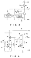
- Fig. 3 is a Bi-MOS signal output circuit, which is a first embodiment of the invention and designed for use in a MOS integrated circuit (IC) used as a bus driver.
- IC MOS integrated circuit
- a power-supply voltage VCC is applied to a node 31.
- the node 31 is connected to the collector of an NPN-type bipolar transistor 32.
- the emitter of the NPN-type bipolar transistor 32 is connected to a node 33, from which a signal OUT will be output.
- the base of the bipolar transistor 32 is connected to a node 34, to which an input signal IN ⁇ is supplied.
- the node 33 is coupled to the collector of an NPN-type bipolar transistor 35.
- the emitter of this bipolar transistor 35 is connected to a node 36, to which a ground potential GND is applied.
- the node 33 is also connected to the drain of an N-channel MOS transistor 37.
- the source of the MOS transistor 37 is coupled to the base of the bipolar transistor 35.
- the gate of the MOS transistor 37 is connected to a node 38, to which an input signal IN is supplied.
- a pull-down circuit 39 is connected between the base of the bipolar transistor 35 and the node 36. The pull-down circuit 39 discharges the base of the bipolar transistor 35 to the ground potential GND after the transistor 35 has been turned off.
- the drain of an N-channel MOS transistor 40 is coupled to the node 33.
- the source of this MOS transistor 40 is connected to the ground potential GND.
- the gate of the transistor 40 is connected to receive the signal output by a control signal generating means or detector circuit 41.
- the detector circuit 41 generates a control signal from the signal OUT from the node 33 and also the input signal IN ⁇ from the node 34.
- the control signal is in a high-impedance state while the signal OUT supplied from the node 33 is falling from a "H" level to a "L” level, is at the "H” level after the signal OUT has become stable at the "L” level, and is at the "L” level after the input signal IN ⁇ has risen to the "H” level.
- the control signal output by the detector circuit 41 is set into the high-impedance state.
- the MOS transistor 40 is, therefore, off.
- the node 33 is fast discharged since the bipolar transistor 35 has great current-accumulating ability.
- the bipolar transistor 35 absorbs the ringing component contained in the output signal OUT since the MOS transistor 40 is off.
- the MOS transistor 40 forms a new discharging path for the node 33, in addition to the discharging path formed of the bipolar transistor 35. In this case, the node 33 is discharged with an extremely large sink current.
- the bipolar transistor 32 When the input signals IN and IN ⁇ change to the "L" level and the “H” level, respectively, the bipolar transistor 32 is turned on. The node 33 is gradually charged with the power-supply potential VCC. As a result of this, the output signal OUT starts rising to the "H” level. At this time, the MOS transistor 37 is cut off, and the control signal output by the detector circuit 41 falls to the "L” level. The node 33 is, therefore, no longer discharged through the discharging path formed of the bipolar transistor 35 and the discharging path formed of the MOS transistor 40. Once the bipolar transistor 35 is cut off, its base is fast discharged to the ground potential GND by means of the pull-down circuit 39. Hence, no DC currents are generated which will flow through the bipolar transistor 32 or the bipolar transistor 35.
- the node 33 is discharged to the "L" level while the bipolar transistor 35 remains on. Therefore, the generating of the ringing component in the output signal OUT can be suppressed well. Further, the signal output circuit has a sufficiently great ability to drive a load since not only the bipolar transistor 35 but also the MOS transistor 40 is turned on, thus discharging the node 33, when the level of the output signal OUT approaches the "L" level. Still further, the circuit consumes as little power as does an ordinary CMOS integrated circuit since a DC current does not always flow between the power-supply potential VCC and the ground potential GND.
- the pull-down circuit 39 is comprised of an N-channel MOS transistor 42.
- the MOS transistor 42 has a drain coupled to the base of the bipolar transistor 35, a source connected to the node 36 applied with the ground potential GND, and a gate coupled to the node 34 supplied with the input signal IN ⁇ .
- the detector circuit 41 comprises two P-channel MOS transistors 43 and 44 and one N-channel MOS transistor 45. The source and gate of the P-channel MOS transistor 43 are coupled to the node 31 applied with the power-supply potential VCC and the node 33 for outputting the signal OUT, respectively.
- the source, drain and gate of the P-channel MOS transistor 44 are coupled to the drain of the MOS transistor 43, the gate of the MOS transistor 40, and the node 34 for receiving the input signal IN ⁇ , respectively.
- the drain, source and gate of the N-channel MOS transistor 45 are coupled to the drain of the MOS transistor 44, the node 36, and the node 34, respectively.
- the MOS transistors 44 and 45 constitute a CMOS inverter 46.
- the P-channel MOS transistor 43 functions as a switch which is controlled by the output signal OUT.
- the source-drain path of this MOS transistor 43 is connected between the inverter 46 and the node 31 applied with the power-supply potential VCC.
- the MOS transistor 42 In operation, when the input signal IN falls to the "L" level, and the MOS transistor 37 is turned of, the MOS transistor 42 is turned on. As a result, the base of the bipolar transistor 35 is discharged to the ground potential GND. Hence the MOS transistor 42 functions as a pull-down circuit.
- the P-channel MOS transistor 43 incorporated in the detector circuit 41 is off while the output signal OUT at the node 33 remains at the "H" level. Hence, even if the input signal IN ⁇ falls to the "L" level, turning on the P-channel MOS transistor 44, the output of the detector circuit 41 remains at high impedance.
- the output signal OUT falls from the power-supply potential VCC to a level below the absolute value of the threshold voltage of the transistor 43, because to the discharging of the bipolar transistor 35, the transistor 43 is turned on, whereby the control signal output by the circuit 41 rises to the "H” level. As a result of this, the MOS transistor 40 is turned on, and cooperates with the bipolar transistor 35 to discharge the node 33.
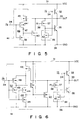
- Fig. 5 illustrates a signal output circuit which is a second embodiment of the present invention.
- the parts which corresponds to those shown in Figs. 3 and 4 are designated in Fig. 5 by like characters, and will not be described. Only the characterizing features of the second embodiment will be described in detail, with reference to Fig. 5.
- the signal output circuit of Fig. 5 is characterized by the detector circuit 41.
- the circuit 41 includes a resistor 47 which is connected between the drain of the P-channel MOS transistor 44 and the node of the drain of the N-channel MOS transistor 45 and the gate of the N-channel MOS transistor 40.
- the resistor 47 adjusts the timing of turning on the transistor 40 while the node 33 is being discharged. The higher the resistance of this resistor 47, the longer it takes to turn on the transistors 43 and 44, and the more slowly the gate of the transistor 40 is charged with the power-supply potential VCC. After all, the higher the resistance of the resistor 47, the more the timing of turning on the transistor 40 is delayed.
- Fig. 6 shows a signal output circuit according to a third embodiment of the present invention.
- the parts which corresponds to those shown in Figs. 3 and 4 are designated in Fig. 6 by like characters, and will not be described.
- the circuit shown in Fig. 6 has a detector circuit 41 which can drive the the gate of the N-channel MOS transistor 40 more efficiently than the detector circuits illustrated in Figs. 4 and 5.
- the detector circuit 41 has an additional component, i.e., a Bi-CMOS inverter comprised of a CMOS inverter 50 and an NPN-type bipolar transistor 51.
- the CMOS inverter 50 is formed of a P-channel MOS transistor 48 and an N-channel MOS transistor 49, and is connected between the drain of a P-channel MOS transistor 43 and a node 36.
- An input signal IN ⁇ is supplied to the input of the CMOS inverter 50.
- the NPN-type bipolar transistor 51 has its collector-emitter path connected between the gate of an N-channel MOS transistor 40 and a node 31 applied with the power-supply potential VCC. The base of the transistor 51 is connected to receive the output of the CMOS inverter 50.
- the combination of the CMOS inverter 50 and the NPN-type bipolar transistor 51 having a great current-accumulating ability serves to prevent an increase in the chip size of the signal output circuit.
- the pull-down circuit 39 is comprised of an N-channel MOS transistor 42.
- the present invention can provide a signal output circuit which has a great ability of driving a load and can yet suppress the ringing component contained in an output signal, and can also provide a signal output circuit which consumes as little power as does a CMOS integrated circuit.
Landscapes
- Engineering & Computer Science (AREA)
- Physics & Mathematics (AREA)
- Computer Hardware Design (AREA)
- Computing Systems (AREA)
- General Engineering & Computer Science (AREA)
- Mathematical Physics (AREA)
- Power Engineering (AREA)
- Logic Circuits (AREA)
- Metal-Oxide And Bipolar Metal-Oxide Semiconductor Integrated Circuits (AREA)
- Electronic Switches (AREA)
Claims (10)
- Signalausgabeschaltung zur Verwendung in einer integrierten MOS-Schaltung, wobei die Signalausgabeschaltung aufweist:einen ersten Schaltungsknoten (33) zur Ausgabe eines Signals (OUT);einen zweiten Schaltungsknoten (36), an welchen ein erstes Stromversorgungsquellenpotential (GND) angelegt wird;einen ersten Bipolartransistor (35) einer ersten Polarität, bei welchem ein Basispfad und ein Kollektor-Emitterpfad zwischen den ersten und den zweiten Schaltungsknoten (33, 36) geschaltet sind;einen ersten MOS-Transistor (37) mit der ersten Polarität, bei welchem ein Sourde-Drain-Pfad zwischen den ersten Schaltungsknoten und die Basis des ersten Bipolartransistors (35) geschaltet ist, und durch ein erstes Eingangssignal (IN) gesteuert wird;einen zweiten MOS-Transistor (40) der ersten Polarität, bei welchem ein Gatepfad und ein Source-Drainpfad zwischen den ersten und zweiten Schaltungsknoten (33, 36) geschaltet ist;einen dritten Schaltungsknoten (31), an welchen ein zweites Stromversorgungsquellenpotential (VCC) angelegt wird;einen zweiten Bipolartransistor (32) der ersten Polarität, bei welchem ein Kollektor-Emitterpfad zwischen den dritten Schaltungsknoten (31) und den ersten Schaltungsknoten (33) geschaltet ist und von einem zweiten Eingangssignal (IN) gesteuert wird; undeine Steuersignalerzeugungsvorrichtung (41), welche auf das Signal (OUT), welches von dem ersten Schaltungsknoten (33) ausgegeben wird, und das zweite Eingangssignal (IN) reagiert, um den zweiten MOS-Transistor (40) in einen Zustand hoher Impedanz zu versetzen, wenn ein Pegel des Signals (OUT), welches von dem ersten Schaltungsknoten ausgegeben wird, von einem hohen Pegel (H) auf einen niedrigen Pegel (L) absinkt, und zum Liefern eines Steuersignals, welches einen Pegel entsprechend dem Pegel des zweiten Eingangssignals (IN) aufweist, an das Gate des zweiten MOS-Transistors (40), wenn der Pegel des Signals (OUT), welches von dem ersten Schaltungsknoten (33) ausgegeben wird, auf den niedrigen Pegel (L) abgesunken ist.
- Schaltung nach Anspruch 1, dadurch gekennzeichnet, daß die Steuersignalerzeugungsvorrichtung (41) eine Signalumkehrungsvorrichtung (46) aufweist, um das zweite Eingangssignal (IN) zu empfangen und ein Ausgangssignal an das Gate des zweiten MOS-Transistors (40) zu liefern, sowie eine Schaltvorrichtung (43) aufweist, die zwischen den dritten Schaltungsknoten (31) und die Signalumkehrvorrichtung (46) geschaltet ist und durch das Signal (OUT) an dem ersten Schaltungsknoten (33) gesteuert wird.
- Schaltung nach Anspruch 2, dadurch gekennzeichnet, daß die Schaltvorrichtung durch einen dritten MOS-Transisotr (43) der zweiten Polarität gebildet wird, bei welchem ein Source-Drain-Pfad zwischen den dritten Schaltungsknoten (31) und die Signalumkehrvorrichtung (46) geschaltet ist, und ein Gate so angeschlossen ist, daß es das Signal (OUT) an dem ersten Schaltungsknoten (33) empfängt.
- Schaltung nach Anspruch 1, dadurch gekennzeichnet, daß die Steuersignalerzeugungsvorrichtung (41) aufweist:einen vierten MOS-Transistor (43) der zweiten Polarität, bei welchem ein Source-Drain-Pfad an einem Ende an den dritten Schaltungsknoten (31) angeschlossen ist, und ein Gate an den ersten Schaltungsknoten (33) angeschlossen ist;einen fünften MOS-Transistor (44) der zweiten Polarität, bei welchem ein Source-Drain-Pfad an einem Ende an das andere Ende des Source-Drain-Pfades des vierten MOS-Transistors (43) angeschlossen ist, und ein Gate so angeschlossen ist, daß es das zweite Eingangssignal (IN) empfängt; undeinen sechsten MOS-Transistor (45) der ersten Polarität, bei welchem ein Source-Drain-Pfad an einem Ende an das andere Ende des fünften MOS-Transistors (44) angeschlossen ist, und an dem anderen Ende an dem zweiten Schaltungsknoten (36), und ein Gate so angeschlossen ist, daß es das zweite Eingangssignal (IN) empfängt.
- Schaltung nach Anspruch 4, dadurch gekennzeichnet, daß zusätzlich ein Widerstand (47) vorgesehen ist, der zwischen das andere Ende des Source-Drain-Pfades des fünften MOS-Transistors (44) und ein Ende des Source-Drain-Pfades des sechsten MOS-Transistors (45) geschaltet ist.
- Schaltung nach Anspruch 1, dadurch gekennzeichnet, daß zusätzlich eine Entladungssteuervorrichtung (39) vorgesehen ist, die zwischen die Bases des ersten Bipolartransistors (35) und den zweiten Schaltungsknoten (36) geschaltet ist, um das Basispotential des ersten Bipolartransistors (35) zu entladen, wenn der erste Bipolartransistor (35) ausgeschaltet wird.
- Schaltung nach Anspruch 6, dadurch gekennzeichnet, daß die Entladungssteuervorrichtung (39) aus einem siebten MOS-Transistor (42) der ersten Polarität besteht, bei welchem ein Source-Drain-Pfad zwischen die Basis des ersten Bipolartransistors (35) und den zweiten Schaltungsknoten (36) geschaltet ist, und ein Gate so angeschlossen ist, daß es das erste Eingangssignal (IN) empfängt.
- Schaltung nach Anspruch 1, dadurch gekennzeichnet, daß die Steuersignalerzeugungsvorrichtung (41) aufweist:eine erste Signalumkehrvorrichtung (46) zum Empfangen des zweiten Signals (IN) und zum Liefern eines Ausgangssignals an das Gate des zweiten MOS-Transistors (40);einen dritten Bipolartransistor (51) der ersten Polarität, bei welchem ein Kollektor-Emitterpfad zwischen den dritten Schaltungsknoten (31) und das Gate des zweiten MOS-Transistors (40) geschaltet ist;eine zweite Signalumkehrvorrichtung (50) zum Empfangen des zweiten Eingangssignals (
 eine Schaltvorrichtung (43), die einerseits an den dritten Schaltungsknoten (31) und andererseits an die erste und zweite Signalumkehrvorrichtung (46, 50) angeschlossen ist und durch das Signal (OUT) an dem ersten Schaltungsknoten (33) gesteuert wird.
 - Schaltung nach Anspruch 8, dadurch gekennzeichnet, daß die Schaltvorrichtung aus einem achten MOS-Transistor (43) der zweiten Polarität besteht, bei welchem ein Source-Drain-Pfad einerseits an den dritten Schaltungsknoten (31) und andererseits an die erste und zweite Signalumkehrvorrichtung (46, 50) angeschlossen ist, und ein Gate so angeschlossen ist, daß es das Signal (OUT) an dem ersten Schaltungsknoten (33) empfängt.
- Schaltung nach Anspruch 1, dadurch gekennzeichnet, daß die Steuersignalerzeugungsvorrichtung (41) aufweist:einen neunten MOS-Transistor (43) der zweiten Polarität, bei welchem ein Source-Drain-Pfad an einem Ende an den dritten Schaltungsknoten (31) angeschlossen ist, und ein Gate mit dem ersten Schaltungsknoten (33) verbunden ist;einen zehnten MOS-Transistor (44) der zweiten Polarität, bei welchem ein Source-Drain-Pfad an einem Ende an das andere Ende des Source-Drain-Pfades des neunten MOS-Transistors (43) angeschlossen ist, und ein Gate so angeschlossen ist, daß es das zweite Eingangssignal (
 einen elften MOS-Transistor (45) der zweiten Polarität, bei welchem ein Source-Drain-Pfad an einem Ende an das andere Ende des Source-Drain-Pfades des zehnten MOS-Transistors (44) angeschlossen ist, und am anderen Ende an den zweiten Schaltungsknoten (36), und ein Gate so angeschlossen ist, daß es das zweite Eingangssignal (
 einen zwölften MOS-Transistor (48) der zweiten Polarität, bei welchem ein Source-Drain-Pfad an einem Ende an das andere Ende des Source-Drain-Pfades des neunten MOS-Transistors (43) angeschlossen ist, und ein Gate so angeschlossen ist, daß es das zweite Eingangssignal (
 einen dreizehnen MOS-Transistor (49) der ersten Polarität, bei welchem ein Source-Drain-Pfad an einem Ende an das andere Ende des Source-Drain-Pfades des zwölften MOS-Transistors (48) angeschlossen ist, und am anderen Ende an den zweiten Schaltungsknoten (36), und ein Gate so angeschlossen ist, daß es das zweite Eingangssignal (
 einen vierten Bipolartransistor (51) der ersten Polarität, der einen Kollektor-Emitter-Pfad aufweist, der zwischen den dritten Schaltungsknoten (31) und das Gate des zweiten MOS-Transistors (40) geschaltet ist, sowie eine Basis, die an das andere Ende des Source-Drain-Pfades des zwölften MOS-Transistors (48) angeschlossen ist.
Applications Claiming Priority (2)
| Application Number | Priority Date | Filing Date | Title |
|---|---|---|---|
| JP1261577A JPH0683058B2 (ja) | 1989-10-06 | 1989-10-06 | 出力回路 |
| JP261577/89 | 1989-10-06 |
Publications (3)
| Publication Number | Publication Date |
|---|---|
| EP0421448A2 EP0421448A2 (de) | 1991-04-10 |
| EP0421448A3 EP0421448A3 (en) | 1991-08-14 |
| EP0421448B1 true EP0421448B1 (de) | 1996-03-13 |
Family
ID=17363852
Family Applications (1)
| Application Number | Title | Priority Date | Filing Date |
|---|---|---|---|
| EP90119103A Expired - Lifetime EP0421448B1 (de) | 1989-10-06 | 1990-10-05 | Ausgangsschaltung mit bipolaren Transistoren im Ausgang, zur Verwendung in einem MOS-IC |
Country Status (5)
| Country | Link |
|---|---|
| US (1) | US5066875A (de) |
| EP (1) | EP0421448B1 (de) |
| JP (1) | JPH0683058B2 (de) |
| KR (1) | KR930007560B1 (de) |
| DE (1) | DE69025844T2 (de) |
Families Citing this family (5)
| Publication number | Priority date | Publication date | Assignee | Title |
|---|---|---|---|---|
| JP2978302B2 (ja) * | 1991-01-28 | 1999-11-15 | 三菱電機株式会社 | 出力バッファ回路 |
| US5331224A (en) * | 1992-08-19 | 1994-07-19 | National Semiconductor Corporation | Icct leakage current interrupter |
| US5534811A (en) * | 1993-06-18 | 1996-07-09 | Digital Equipment Corporation | Integrated I/O bus circuit protection for multiple-driven system bus signals |
| US5748022A (en) * | 1995-10-31 | 1998-05-05 | Texas Instruments Incorporated | Input circuit |
| US6300815B1 (en) * | 2000-01-31 | 2001-10-09 | Texas Instruments Incorporated | Voltage reference overshoot protection circuit |
Family Cites Families (5)
| Publication number | Priority date | Publication date | Assignee | Title |
|---|---|---|---|---|
| EP0209805B1 (de) * | 1985-07-22 | 1993-04-07 | Hitachi, Ltd. | Halbleitereinrichtung mit bipolarem Transistor und Isolierschicht-Feldeffekttransistor |
| JPS62221219A (ja) * | 1986-03-22 | 1987-09-29 | Toshiba Corp | 論理回路 |
| JPS63202126A (ja) * | 1987-02-17 | 1988-08-22 | Toshiba Corp | 論理回路 |
| US4933574A (en) * | 1989-01-30 | 1990-06-12 | Integrated Device Technology, Inc. | BiCMOS output driver |
| EP0387461A1 (de) * | 1989-03-14 | 1990-09-19 | International Business Machines Corporation | BICMOS-Schaltung mit vollem Spannungshub für logische Signale |
-
1989
- 1989-10-06 JP JP1261577A patent/JPH0683058B2/ja not_active Expired - Lifetime
-
1990
- 1990-10-03 US US07/592,236 patent/US5066875A/en not_active Expired - Lifetime
- 1990-10-05 DE DE69025844T patent/DE69025844T2/de not_active Expired - Fee Related
- 1990-10-05 EP EP90119103A patent/EP0421448B1/de not_active Expired - Lifetime
- 1990-10-06 KR KR1019900015892A patent/KR930007560B1/ko not_active Expired - Fee Related
Also Published As
| Publication number | Publication date |
|---|---|
| JPH03123220A (ja) | 1991-05-27 |
| EP0421448A2 (de) | 1991-04-10 |
| US5066875A (en) | 1991-11-19 |
| KR910008959A (ko) | 1991-05-31 |
| KR930007560B1 (ko) | 1993-08-12 |
| JPH0683058B2 (ja) | 1994-10-19 |
| DE69025844D1 (de) | 1996-04-18 |
| EP0421448A3 (en) | 1991-08-14 |
| DE69025844T2 (de) | 1996-08-22 |
Similar Documents
| Publication | Publication Date | Title |
|---|---|---|
| EP0329285B1 (de) | Ausgangspuffer | |
| JP3618829B2 (ja) | ノイズの影響を受けないリセット優先レベルシフト回路 | |
| US6624672B2 (en) | Output buffer with constant switching current | |
| US4902914A (en) | Logic circuit used in standard IC or CMOS logic level | |
| US6121789A (en) | Output buffer with control circuitry | |
| EP0260389A2 (de) | Chip-Ausgangsschnittstellenschaltung | |
| US7034571B2 (en) | Level converting circuit efficiently increasing an amplitude of a small-amplitude signal | |
| JPH057931B2 (de) | ||
| JPH04229714A (ja) | バッファを有する集積回路 | |
| US5930129A (en) | Power on reset circuit | |
| US6249146B1 (en) | MOS output buffer with overvoltage protection circuitry | |
| EP0351820A2 (de) | Ausgangschaltung | |
| EP0768762B1 (de) | Ausgangsschaltung | |
| US4612458A (en) | Merged PMOS/bipolar logic circuits | |
| US5066875A (en) | Signal output circuit having bipolar transistors at output, for use in a mos semiconductor integrated circuit | |
| US7075335B2 (en) | Level shifter | |
| US6833749B2 (en) | System and method for obtaining hysteresis through body substrate control | |
| US5442304A (en) | CMOS logic gate clamping circuit | |
| US6756814B2 (en) | Logic circuit and semiconductor device | |
| JPH0677804A (ja) | 出力回路 | |
| EP0735686B1 (de) | CMOS Ausgangspuffer mit drei Zuständen | |
| US5408136A (en) | Circuit for providing fast logic transitions | |
| JP3339410B2 (ja) | ドライバ回路 | |
| JP3512641B2 (ja) | レベルシフト回路および半導体集積回路 | |
| KR20040005091A (ko) | 출력 버퍼 |
Legal Events
| Date | Code | Title | Description |
|---|---|---|---|
| PUAI | Public reference made under article 153(3) epc to a published international application that has entered the european phase |
Free format text: ORIGINAL CODE: 0009012 |
|
| 17P | Request for examination filed |
Effective date: 19901005 |
|
| AK | Designated contracting states |
Kind code of ref document: A2 Designated state(s): DE FR GB |
|
| PUAL | Search report despatched |
Free format text: ORIGINAL CODE: 0009013 |
|
| AK | Designated contracting states |
Kind code of ref document: A3 Designated state(s): DE FR GB |
|
| 17Q | First examination report despatched |
Effective date: 19940502 |
|
| GRAA | (expected) grant |
Free format text: ORIGINAL CODE: 0009210 |
|
| AK | Designated contracting states |
Kind code of ref document: B1 Designated state(s): DE FR GB |
|
| REF | Corresponds to: |
Ref document number: 69025844 Country of ref document: DE Date of ref document: 19960418 |
|
| ET | Fr: translation filed | ||
| PLBE | No opposition filed within time limit |
Free format text: ORIGINAL CODE: 0009261 |
|
| STAA | Information on the status of an ep patent application or granted ep patent |
Free format text: STATUS: NO OPPOSITION FILED WITHIN TIME LIMIT |
|
| 26N | No opposition filed | ||
| REG | Reference to a national code |
Ref country code: GB Ref legal event code: IF02 |
|
| PGFP | Annual fee paid to national office [announced via postgrant information from national office to epo] |
Ref country code: DE Payment date: 20070927 Year of fee payment: 18 |
|
| PGFP | Annual fee paid to national office [announced via postgrant information from national office to epo] |
Ref country code: GB Payment date: 20071003 Year of fee payment: 18 Ref country code: FR Payment date: 20071009 Year of fee payment: 18 |
|
| GBPC | Gb: european patent ceased through non-payment of renewal fee |
Effective date: 20081005 |
|
| REG | Reference to a national code |
Ref country code: FR Ref legal event code: ST Effective date: 20090630 |
|
| PG25 | Lapsed in a contracting state [announced via postgrant information from national office to epo] |
Ref country code: DE Free format text: LAPSE BECAUSE OF NON-PAYMENT OF DUE FEES Effective date: 20090501 |
|
| PG25 | Lapsed in a contracting state [announced via postgrant information from national office to epo] |
Ref country code: FR Free format text: LAPSE BECAUSE OF NON-PAYMENT OF DUE FEES Effective date: 20081031 |
|
| PG25 | Lapsed in a contracting state [announced via postgrant information from national office to epo] |
Ref country code: GB Free format text: LAPSE BECAUSE OF NON-PAYMENT OF DUE FEES Effective date: 20081005 |