EP0421449A2 - Répéteur optique avec circuit d'inversion de phase - Google Patents
Répéteur optique avec circuit d'inversion de phase Download PDFInfo
- Publication number
- EP0421449A2 EP0421449A2 EP90119104A EP90119104A EP0421449A2 EP 0421449 A2 EP0421449 A2 EP 0421449A2 EP 90119104 A EP90119104 A EP 90119104A EP 90119104 A EP90119104 A EP 90119104A EP 0421449 A2 EP0421449 A2 EP 0421449A2
- Authority
- EP
- European Patent Office
- Prior art keywords
- signal
- phase
- optical
- supervisory
- extracting
- Prior art date
- Legal status (The legal status is an assumption and is not a legal conclusion. Google has not performed a legal analysis and makes no representation as to the accuracy of the status listed.)
- Ceased
Links
Images




Classifications
-
- H—ELECTRICITY
- H04—ELECTRIC COMMUNICATION TECHNIQUE
- H04B—TRANSMISSION
- H04B10/00—Transmission systems employing electromagnetic waves other than radio-waves, e.g. infrared, visible or ultraviolet light, or employing corpuscular radiation, e.g. quantum communication
- H04B10/29—Repeaters
Definitions
- the present invention generally relates to an optical repeater provided in an optical communication system, such as an optical submarine (undersea) repeater. More particularly, the present invention relates to an optical repeater having a phase inversion circuit designed to invert the phase of an optical input signal in digital form and output an optical signal having the inverted phase.
- the reduction of a transmission loss of an optical fiber makes it possible to increase an interval at which adjacent repeaters are arranged, so that a long-distance transmission of optical signals can be easily realized.
- a long-distance transmission of optical signals there is a problem of systematic jitter accumulation arising from an arrangement in which an optical signal passes through a plurality of repeaters.
- FIG. 1 there is illustrated a conventional optical repeater.
- the optical repeater shown in FIG. 1 composed of an opto-electric converter 2 connected to an optical transmission line 1, an equalizing amplifier 3, a timing extraction circuit 4, a D-type flip-flop 5, a driving circuit 6, an electro-optical converter 7 coupled to an optical transmission line 8, a frequency divider 9 and a bandpass filter 10.
- An optical digital signal via the optical transmission line 1 is converted into an electrical signal by the opto-electric converter 2.
- the equalizing amplifier 3 amplifies and equalizes the electrical signal from the opt-electric converter 2.
- An output signal of the equalizing amplifier 3 is input to a terminal D of the flip-flop 5 and the timing extraction circuit 4.
- the timing extraction circuit 4 generates a timing signal from the output signal from the equalizing amplifier 3.
- the timing signal generated by the timing extraction circuit 4, which is synchronized with the optical digital signal, is applied to a clock terminal C of the flip-flop 5.
- the output signal of the equalizing amplifier 3 is latched in synchronism with the timing signal, and a regenerated digital signal is output via a terminal Q of the flip-flop 5.
- the reproduced dital signal is input to the driving circuit 6 and the frequency divider 9.
- the driving circuit 6 drives a laser diode provided in the electro-optical converter 7, which output a regenerated and amplified optical digital signal to the transmission line 8.
- the frequency divider 9 has a flip-flop, which generates a signal having a frequency half the frequency of the signal output from the flip-flop 5.
- the signal generated and output by the frequency divider 9 passes through the bandpass filter 10, which generates a supervisory signal.
- the optical digital signal is transmitted via the optical transmission lines 1 and 8 in the form of a 25B1P code.
- the 24B1P code is composed of 24 data bits and a one-bit parity P relative to the 24 data bits. One block is formed of these 25 bits.
- the output signal of the flip-flop is always equal to "0" at the end of one block, because the number of "1" is even.
- the initial state of the flip-flop of the frequency divider 9 is equal to "1" and no bit error occurs, the output signal of the flip-flop is always equal to "1".
- symbol BL denotes one block
- T denotes a predetermined period during which a plurality of blocks, each having the even parity, are transmitted. Odd parities are inserted at intervals corresponding to the predetermined period T. That is, one odd parity is inserted for every period T.
- the output signal of the frequency divider 9 is inverted each time and odd parity is applied thereto. In other words, the flip-flop of the frequency divider 9 changes its status each time the odd parity is applied thereto (for every period T).
- the bandpass filter 6 has a bandpass range having a central frequency substantially corresponding to the reciprocal of the period T, and extracts signal components in the bandpass range. Thus, it is possible to superimpose a low-bit rate supervisory signal on a high-speed data signal and extract this supervisory signal by the combination of the frequency divider 9 and the bandpass filter 10.
- the repeated optical signal output from each repeater has the same phase as the optical signal input to each repeater. That is, logic “1" of the input signal is transmitted as it is (logic "1").
- a single-mode semiconductor laser diode such as a DFB (distributed feedback laser diode)
- a wavelength shift occurs at the rise and fall of a driving current applied to the laser diode.
- An optical signal having such a wavelength shift is affected by the wavelength distribution characteristics of the optical transmission lines 1 and 8, so that variations in the rise and fall of the optical signal on the time base, that is, systematic jitter is caused.
- a more specific object of the present invention is to provide an optical repeater capable of effectively suppressing systematic jitter and easily extracting a supervisory or command signal superimposed on optical signals transmitted via transmission lines.
- an optical repeater comprising a first converter converting an optical input signal into an electrical signal, an equalizing amplifier which amplifies the electrical signal and which outputs an amplified electrical signal, and a timing extraction circuit which extracts a timing signal from the amplified electrical signal.
- the optical repeater includes a phase inversion circuit which receives the amplified electrical signal in synchronism with the timing signal and which outputs a phase-inverted signal in synchronism with the timing signal.
- the phase-inverted signal has a phase opposite to a phase of the amplified electrical signal.
- the optical repeater includes a second converter having a diffused laser diode and converting the phase-inverted signal into an optical output signal, and supervisory signal extraction circuit which extracts a supervisory signal contained in the optical input signal from the phase-inverted signal.
- the optical input signal includes a digital signal formed of a plurality of blocks. Each block has data composed of (2m+1) bit (where m is an integer) and one-bit parity so that each block is formed of a (2m+1) B1P code having an event parity.
- an optical repeater comprising: first converter means for converting an optical input signal into an electrical signal; equalizing amplifier means, coupled to the first converter means, for amplifying the electrical signal and for outputting an amplified electrical signal; timing extraction means, coupled to the equalizing amplifier means, for extracting a timing signal from the amplified electrical signal; phase inversion means, coupled to the equalizing amplifier and the timing extraction means, for receiving the amplified electrical signal in synchronism with the timing signal and for outputting an in-phase signal and a phase inverted signal in synchronism with the timing signal, the in-phase signal being in phase with the amplified electrical signal, and the phase-inverted signal having a phase opposite to a phase of the amplified electrical signal; second converting means, coupled to the phase inversion means, for converting the phase-inverted signal into an optical output signal; and supervisory signal extracting means, coupled to the phase inversion means, for extracting a supervisory signal contained in the optical input signal from one of the in
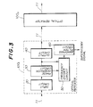
- An optical transmission system shown in FIG.3 includes a plurality of optical repeaters 1001, ..., 100 n (n is an integer) provided in an optical transmission line 11 such as an optical fiber cable.
- Each of the optical repeaters 1001, ..., 100 n is composed of an input circuit 20, a phase inversion circuit 30, an output circuit 40, a frequency divider circuit 50 and a bandpass filter circuit 60.
- the input circuit 20 is composed of an opto-electric converter 21, an equalizing amplifier 22 and a timing generator 23, which correspond to the opto-electric converter 2, the equalizing amplifier 3 and the timing generation circuit 4 shown in FIG.1 respectively.
- the opto-electric converter 2 is formed of, for example, an avalanche diode.
- the phase inversion circuit 30 has a D-type flip-flop 31.
- the output circuit 40 is composed of a driving circuit 41 and an electro-optical converter 42, which correspond to the driving circuit 6 and the electro-optical converter 7 shown in FIG.1, respectively.
- the electro-optical converter 42 is formed of, for example, DFB laser diode.
- the flip-flop 31 of the phase inversion circuit 30 has a data terminal D, a clock terminal C, and two output terminals Q and Q .
- An output terminal of the equalizing amplifier 22 is connected to the data terminal D of the flip-flop 31, and an output terminal of the timing extraction circuit 23 is connected to the clock terminal C thereof.
- the terminal Q of the flip-flop 31 is connected to an input terminal of the driving circuit 41 of the output circuit 40. Conventionally, as shown in FIG.1, the terminal Q of the flip-flop 9 is connected to the driving circuit 6.
- An incoming optical digital signal via the transmission line 11 is converted into an electrical signal by the opto-electric converter 21.
- the electrical signal generated and output by the opto-electric converter 21 is equalized and amplified by the equalizing amplifier 22.
- An equalized and amplified signal from the equalizing amplifier 22 is input to the data terminal D of the flip-flop 31 of the phase inversion circuit 30.
- the equalized and amplified signal from the equalizing amplifier 22 is input to the timing extraction circuit 23, which outputs a timing signal synchronized with the optical digital signal to the clock terminal C of the flip-flop 31.
- a signal (phase-inverted signal) at the terminal Q of the flip-flop 31 has a phase opposite to the phase of the signal at the data terminal D thereof.
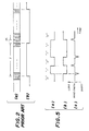
- the optical signal which penetrates in the optical transmission line 11 has been amplitude-modulated.
- the optical digital signal has been amplitude-modulated in accordance with data "0", "1", “0", “1", “1” and "0".
- the optical repeater 1001 outputs an optical output signal in digital form shown in FIG.5-(b) when the optical input signal shown in FIG.5-(a) is input thereto.
- the optical output signal in FIG.5-(b) has a phase opposite to that of the optical input signal in FIG.5-(a).
- FIG.5-(c) illustrates a variation in the wavelength of the optical output signal.
- the wavelength of the optical output signal changes toward a short wavelength in response to the fall of the optical output signal.
- the wavelength of the optical output signal changes toward a long wavelength in response to the rise of the optical output signal.
- the rise timing of the optical digital signal which is input to the optical repeater being considered corresponds to the fall timing of the optical digital signal which is output therefrom.
- a waveform variation caused when the optical digital signal input to the optical repeater rises is cancelled by a waveform variation caused when the optical digital signal output therefrom falls.
- the phase of the optical digital signal sent by the terminal equipment device on the transmission side is the same as that of the optical digital signal received by the receive-side terminal equipment device via the even number of optical repeaters.
- the phase of the optical digital signal on the transmission side is opposite to that of the optical digital signal on the receive side. In this case, it is preferable to provide the receive-side terminal equipment device with a circuit designed to change the phase of the received optical digital signal.
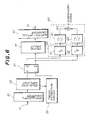
- FIG.6 illustrates the configuration of the frequency divider circuit 50 and the bandpass filter circuit 60 shown in FIG.3 together with the other arrangement shown in FIG.4.
- the frequency divider circuit 50 is composed of two frequency dividers 51 and 52.
- the frequency divider 51 has an input terminal connected to the terminal Q of the flip-flop 31 of the phase inversion circuit 30, and an output terminal.
- the frequency divider 52 has an input terminal connected to the terminal Q of the flip-flop 31 and an output terminal.
- phase of the signal at the data terminal D of the flip-flop 31 is the same as that of the signal (in phase signal) at the terminal Q thereof, and opposite to that of the signal (phase-inverted signal) at the terminal Q thereof.
- Each of the frequency dividers 51 and 52 divides the frequency of the corresponding input signal by 2. That is, each of the frequency dividers 51 and 52 generates an output signal having a frequency half the frequency of the signal applied thereto.
- the bandpass filter circuit 60 is composed of bandpass filters 61 and 62, and an adder 63.
- the bandpass filters 61 and 62 have input terminals respectively connected to the output terminals of the frequency dividers 51 and 52, and output terminals respectively connected to first and second input terminals of the adder 63.
- phase-inverted digital signal is output from the terminal Q of the flip-flop 25.
- the phase-inverted digital signal at the terminal Q of the flip-flop 25 has the phase identical to the phase on the transmission side.
- This phase-inverted digital signal is input to the frequency divider 52, which generates a signal having a frequency half that of the phase-inverted digital signal.
- the signal generated and output by the frequency divider 52 passes through the bandpass filter 62, which outputs a supervisory or command signal having a period such as shown in FIG.2.
- the supervisory or command signal is used for monitoring the status of predetermined devices in the optical repeater and sending information about the monitored status to the terminal on the transmission or reception side.
- the output signal generated and output by the the frequency divider 51 has less supervisory signal component.
- the adder 63 outputs the supervisory signal extracted by the bandpass filter 62.
- the supervisory signal is extracted by the combination of the frequency divider 51 and the bandpass filter 61 of each odd-numbered optical repeater, and on the other hand, the supervisory signal is extracted by the combination of the frequency divider 52 and the bandpass filter 62 of each even-numbered optical repeater.
- FIG.7 illustrates the structure of the frequency divider circuit 50 and the bandpass filter circuit 60 according to the second embodiment of the present invention.
- the frequency divider circuit 50 shown in FIG.7 is composed of frequency dividers 53 and 54, each having the same function as that of the frequency dividers 51 and 52 shown in FIG.6.
- the bandpass filter circuit 60 shown in FIG.6 is composed of an adder 64 and a single bandpass filter 65, which has the same function as each of the bandpass filters 61 and 62.
- the output terminals of the frequency dividers 53 and 54 are connected to first and second input terminals of the adder 64, respectively.
- the output terminal of the adder 64 is connected to the input terminal of the bandpass filter 65.
- the bandpass filter 65 is used in common for the frequency dividers 53 and 54.
- the configuration shown in FIG.7 is more economical than the configuration shown in FIG.6.
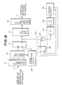
- FIG.8 A description will now be given of a third preferred embodiment of the present invention with reference to FIG.8.
- FIG.8 those parts which are the same as those shown in FIG.4 are given the same reference numerals.
- the input circuit 20, the phase inversion circuit 30 and the output circuit 40 shown in FIG.8 are the same as corresponding those shown in FIG.4.
- the optical repeater shown in FIG.8 is further composed of a frequency divider 55, a bandpass filter 66, a control circuit 70 and a switch circuit 80.
- the switch circuit 80 has two modes of first and second modes. In the first mode, the switch circuit 80 passes the phase-inverted output signal from the terminal Q of the flip-flop 31 without changing the phase thereof. In the second mode, the switch circuit 80 inverts the phase of the phase-inverted output signal from the terminal Q of the flip-flop 31. The switch circuit 80 selects one of the first and second modes in accordance with a switch control signal, which is generated and output by the control circuit 70. The control circuit 70 receives a supervisory signal from the bandpass filter 66.
- the switch circuit 80 is composed of an exclusive-OR gate 81 and an RS-type flip-flop 82.
- the exclusive-OR has two input terminals, one of which being connected to the terminal Q of the flip-flop 31, and the other input terminal being connected to a terminal Q of the flip-flop 82.
- the exclusive-OR gate 81 has an output terminal connected to the input terminal of the frequency divider 55.
- the flip-flop 82 has a set terminal S and a reset terminal R, both of which are supplied with switching control signals generated and output by the control circuit 70.
- the flip-flop 82 When the power supply to an optical communication system having the optical repeater shown in FIG.8 is turned ON, the flip-flop 82 is set to an initial state (reset or set state) due to a power ON reset function. For example, the terminal Q of the flip-flop 82 is set to a logically low level ("0"). Then, an optical signal having a command (supervisory) signal addressed to the optical repeater being considered is transmitted. If the optical signal being considered handles the non-inverted signal (having the same phase as the optical signal sent by the transmission side), the command signal is not extracted from the bandpass filter 66 where the flip-flop 82 is at the low level. In this case, an optical signal having an inverted command signal is transmitted.
- the optical repeater being considered receives the optical signal having the inverted command signal, and the command signal is output from the bandpass filter 66.
- the control circuit 70 decodes the command signal, and sends the control signal so that the state of the flip-flop 82 is changed. Thereby, the terminal Q of the flip-flop 82 is switched to a logically high level ("1"). As a result, an inverted version of the output signal obtained at the terminal Q of the flip-flop 31 is applied to the frequency divider 55.
- FIG.9 A description will now be given of a fourth embodiment of the present invention with reference to FIGS.9 and 10.
- the configuration shown in FIG.9 is obtained by adding a frequency divider 56 and a bandpass filter 57 to the configuration shown in FIG.4.
- the frequency divider 56 has an input terminal connected to the terminal Q of the flip-flop 31.
- a one-bit parity P is added to data composed of (2m+1) bits, and a block having the even parity is transmitted.
- m is not limited to these values.
Landscapes
- Physics & Mathematics (AREA)
- Electromagnetism (AREA)
- Engineering & Computer Science (AREA)
- Computer Networks & Wireless Communication (AREA)
- Signal Processing (AREA)
- Optical Communication System (AREA)
- Dc Digital Transmission (AREA)
Applications Claiming Priority (4)
| Application Number | Priority Date | Filing Date | Title |
|---|---|---|---|
| JP262455/89 | 1989-10-06 | ||
| JP26245589 | 1989-10-06 | ||
| JP101691/90 | 1990-04-19 | ||
| JP2101691A JPH0738648B2 (ja) | 1989-10-06 | 1990-04-19 | 光信号中継伝送制御方式 |
Publications (2)
| Publication Number | Publication Date |
|---|---|
| EP0421449A2 true EP0421449A2 (fr) | 1991-04-10 |
| EP0421449A3 EP0421449A3 (en) | 1992-12-09 |
Family
ID=26442522
Family Applications (1)
| Application Number | Title | Priority Date | Filing Date |
|---|---|---|---|
| EP19900119104 Ceased EP0421449A3 (en) | 1989-10-06 | 1990-10-05 | Optical repeater having phase inversion circuit |
Country Status (4)
| Country | Link |
|---|---|
| US (1) | US5097353A (fr) |
| EP (1) | EP0421449A3 (fr) |
| JP (1) | JPH0738648B2 (fr) |
| CA (1) | CA2027051C (fr) |
Cited By (2)
| Publication number | Priority date | Publication date | Assignee | Title |
|---|---|---|---|---|
| WO2001013550A1 (fr) * | 1999-08-18 | 2001-02-22 | Fujitsu Network Communications, Inc. | Regenerateur conservant la longueur d'onde pour systemes de transmission a multiplexage en longueur d'onde dense |
| EP0975105A3 (fr) * | 1998-07-23 | 2001-03-21 | Nec Corporation | Procédé et dispositif de regéneration et de relais d'un signal transmis optique et système de transmission optique par multiplexage à longueur d'onde les utilisant |
Families Citing this family (14)
| Publication number | Priority date | Publication date | Assignee | Title |
|---|---|---|---|---|
| US5309475A (en) * | 1991-10-01 | 1994-05-03 | Abb Power T&D Company Inc. | Data interchange network |
| US5392147A (en) * | 1991-10-21 | 1995-02-21 | Nec Corporation | Optical trunk transmission system and an optical repeater circuit |
| US5847694A (en) * | 1991-12-05 | 1998-12-08 | Tv Interactive Data Corporation | Apparatus for generating a signal indicative of the position of a movable element in the apparatus |
| US5650608A (en) * | 1991-12-05 | 1997-07-22 | Tv Interactive Data Corporation | Method and apparatus for generating ratiometric control signals |
| JP2771071B2 (ja) * | 1992-04-23 | 1998-07-02 | 日立造船株式会社 | 中継局を経由する伝送方法 |
| JP2986613B2 (ja) * | 1992-05-27 | 1999-12-06 | 株式会社日立製作所 | 光伝送モジュール |
| US5400360A (en) * | 1993-03-23 | 1995-03-21 | Limitorque Corporation | Repeater for a digital control system |
| EP0721708B1 (fr) * | 1993-09-30 | 1999-03-24 | ANT Nachrichtentechnik GmbH | Procede de transmission optique de messages et repeteurs intermediaires utilises a cet effet |
| US5629789A (en) * | 1994-05-02 | 1997-05-13 | Lucent Technologies Inc. | Passive optical repeater bypass for optical fiber systems |
| EP0772863A4 (fr) * | 1994-07-26 | 1997-10-01 | Tv Interactive Data Corp | Dispositif de commande a detecteur de position et procede pour generer des signaux de commande |
| US5818037A (en) * | 1996-04-09 | 1998-10-06 | Tv Interactive Data Corporation | Controller using a flexible element to vary light transferred to a photosensitive element |
| SE9604214L (sv) * | 1996-11-18 | 1998-05-19 | Ericsson Telefon Ab L M | Förfarande och anordning inom telekommunikation |
| DE10039951C2 (de) * | 2000-08-16 | 2002-10-10 | Siemens Ag | Verfahren und Anordnung zur Kompensation von Kreuzphasenmodulation |
| US11327226B2 (en) | 2019-04-22 | 2022-05-10 | California Institute Of Technology | Integrated photonics long-distance sensing system |
Family Cites Families (5)
| Publication number | Priority date | Publication date | Assignee | Title |
|---|---|---|---|---|
| JPS594256A (ja) * | 1982-06-29 | 1984-01-11 | Fujitsu Ltd | Pcm信号中継器監視方式 |
| JPS60241351A (ja) * | 1984-05-16 | 1985-11-30 | Kokusai Denshin Denwa Co Ltd <Kdd> | 光中継器監視方式 |
| FR2577088B1 (fr) * | 1985-02-07 | 1987-03-06 | Thomson Csf Mat Tel | Repeteur pour distribution d'horloge tripliquee |
| JPS62210747A (ja) * | 1986-03-12 | 1987-09-16 | Matsushita Electric Ind Co Ltd | 光伝送装置 |
| JP2711670B2 (ja) * | 1988-03-11 | 1998-02-10 | 富士通株式会社 | 中継器監視方式 |
-
1990
- 1990-04-19 JP JP2101691A patent/JPH0738648B2/ja not_active Expired - Lifetime
- 1990-10-03 US US07/592,365 patent/US5097353A/en not_active Expired - Fee Related
- 1990-10-05 CA CA002027051A patent/CA2027051C/fr not_active Expired - Fee Related
- 1990-10-05 EP EP19900119104 patent/EP0421449A3/en not_active Ceased
Cited By (3)
| Publication number | Priority date | Publication date | Assignee | Title |
|---|---|---|---|---|
| EP0975105A3 (fr) * | 1998-07-23 | 2001-03-21 | Nec Corporation | Procédé et dispositif de regéneration et de relais d'un signal transmis optique et système de transmission optique par multiplexage à longueur d'onde les utilisant |
| WO2001013550A1 (fr) * | 1999-08-18 | 2001-02-22 | Fujitsu Network Communications, Inc. | Regenerateur conservant la longueur d'onde pour systemes de transmission a multiplexage en longueur d'onde dense |
| US6476953B1 (en) | 1999-08-18 | 2002-11-05 | Fujitsu Network Communications, Inc. | Wavelength preserving regenerator for DWDM transmission systems |
Also Published As
| Publication number | Publication date |
|---|---|
| CA2027051C (fr) | 1993-10-05 |
| JPH0738648B2 (ja) | 1995-04-26 |
| US5097353A (en) | 1992-03-17 |
| EP0421449A3 (en) | 1992-12-09 |
| JPH03205938A (ja) | 1991-09-09 |
| CA2027051A1 (fr) | 1991-04-07 |
Similar Documents
| Publication | Publication Date | Title |
|---|---|---|
| US5097353A (en) | Optical repeater having phase inversion circuit | |
| US5200979A (en) | High speed telecommunication system using a novel line code | |
| EP1830532B1 (fr) | Circuit précodé et circuit de multiplexage à précodage pour effectuer un taux de transmission très élevé dans une communication à fibre optique | |
| US4584720A (en) | Optical communication system using pulse position modulation | |
| US4415984A (en) | Synchronous clock regenerator for binary serial data signals | |
| US4677608A (en) | Method of transferring an additional information channel across a transmission medium | |
| JPH05268168A (ja) | 光信号伝送方法 | |
| EP0159720B1 (fr) | Système de communication bidirectionnelle de signaux numériques | |
| US3899429A (en) | Pulse-frequency-modulation signal transmission system | |
| US5436752A (en) | Receive-side circuit for a system for optically transmitting a digital signal over a dispersive optical waveguide | |
| GB2240683A (en) | Long-distance high-speed optical communication scheme | |
| CA2031494C (fr) | Systeme de transmission a codes a correlation | |
| US6295318B1 (en) | Method and system for increasing the data rate over twisted copper pairs and other bandwidth-limited dedicated communications facilities | |
| Bendelli et al. | Performance assessment of a photonic ATM switch based on a wavelength-controlled fiber loop buffer | |
| US6542276B1 (en) | Method and apparatus for increasing the spectral efficiency of dense wavelength division multiplexed systems | |
| JPH11127120A (ja) | 光ネットワークにおける符号化および光スイッチ制御方式 | |
| US3588715A (en) | Regenerative repeatered transmission apparatus | |
| WO2024038543A1 (fr) | Dispositif de génération de signal modulé optiquement et module de transmission | |
| JP3838087B2 (ja) | 光通信システム及び光通信装置 | |
| EP0271117B1 (fr) | Génération d'horloge dans un système de transmission ayant une forte limitation de la largeur de bande | |
| US5703645A (en) | Video signal transmitting apparatus | |
| JPH01258531A (ja) | 光中継器監視方式 | |
| JPS6333814B2 (fr) | ||
| SU788424A1 (ru) | Устройство дл приема и передачи дискретных сигналов | |
| JPS622751A (ja) | デ−タ通信装置 |
Legal Events
| Date | Code | Title | Description |
|---|---|---|---|
| PUAI | Public reference made under article 153(3) epc to a published international application that has entered the european phase |
Free format text: ORIGINAL CODE: 0009012 |
|
| AK | Designated contracting states |
Kind code of ref document: A2 Designated state(s): DE FR GB |
|
| PUAL | Search report despatched |
Free format text: ORIGINAL CODE: 0009013 |
|
| AK | Designated contracting states |
Kind code of ref document: A3 Designated state(s): DE FR GB |
|
| 17P | Request for examination filed |
Effective date: 19921229 |
|
| 17Q | First examination report despatched |
Effective date: 19941222 |
|
| GRAG | Despatch of communication of intention to grant |
Free format text: ORIGINAL CODE: EPIDOS AGRA |
|
| STAA | Information on the status of an ep patent application or granted ep patent |
Free format text: STATUS: THE APPLICATION HAS BEEN REFUSED |
|
| 18R | Application refused |
Effective date: 19961230 |