EP0421507A2 - Verfahren zur Herstellung eines bipolaren Transistors - Google Patents
Verfahren zur Herstellung eines bipolaren Transistors Download PDFInfo
- Publication number
- EP0421507A2 EP0421507A2 EP90202437A EP90202437A EP0421507A2 EP 0421507 A2 EP0421507 A2 EP 0421507A2 EP 90202437 A EP90202437 A EP 90202437A EP 90202437 A EP90202437 A EP 90202437A EP 0421507 A2 EP0421507 A2 EP 0421507A2
- Authority
- EP
- European Patent Office
- Prior art keywords
- region
- layer
- impurities
- insulating
- forming
- Prior art date
- Legal status (The legal status is an assumption and is not a legal conclusion. Google has not performed a legal analysis and makes no representation as to the accuracy of the status listed.)
- Granted
Links
Images


Classifications
-
- H—ELECTRICITY
- H10—SEMICONDUCTOR DEVICES; ELECTRIC SOLID-STATE DEVICES NOT OTHERWISE PROVIDED FOR
- H10D—INORGANIC ELECTRIC SEMICONDUCTOR DEVICES
- H10D30/00—Field-effect transistors [FET]
- H10D30/01—Manufacture or treatment
- H10D30/021—Manufacture or treatment of FETs having insulated gates [IGFET]
- H10D30/0223—Manufacture or treatment of FETs having insulated gates [IGFET] having source and drain regions or source and drain extensions self-aligned to sides of the gate
- H10D30/0227—Manufacture or treatment of FETs having insulated gates [IGFET] having source and drain regions or source and drain extensions self-aligned to sides of the gate having both lightly-doped source and drain extensions and source and drain regions self-aligned to the sides of the gate, e.g. lightly-doped drain [LDD] MOSFET or double-diffused drain [DDD] MOSFET
-
- H—ELECTRICITY
- H10—SEMICONDUCTOR DEVICES; ELECTRIC SOLID-STATE DEVICES NOT OTHERWISE PROVIDED FOR
- H10W—GENERIC PACKAGES, INTERCONNECTIONS, CONNECTORS OR OTHER CONSTRUCTIONAL DETAILS OF DEVICES COVERED BY CLASS H10
- H10W20/00—Interconnections in chips, wafers or substrates
- H10W20/01—Manufacture or treatment
- H10W20/031—Manufacture or treatment of conductive parts of the interconnections
- H10W20/069—Manufacture or treatment of conductive parts of the interconnections by forming self-aligned vias or self-aligned contact plugs
-
- H—ELECTRICITY
- H10—SEMICONDUCTOR DEVICES; ELECTRIC SOLID-STATE DEVICES NOT OTHERWISE PROVIDED FOR
- H10D—INORGANIC ELECTRIC SEMICONDUCTOR DEVICES
- H10D10/00—Bipolar junction transistors [BJT]
- H10D10/01—Manufacture or treatment
- H10D10/051—Manufacture or treatment of vertical BJTs
-
- H—ELECTRICITY
- H10—SEMICONDUCTOR DEVICES; ELECTRIC SOLID-STATE DEVICES NOT OTHERWISE PROVIDED FOR
- H10D—INORGANIC ELECTRIC SEMICONDUCTOR DEVICES
- H10D30/00—Field-effect transistors [FET]
- H10D30/60—Insulated-gate field-effect transistors [IGFET]
- H10D30/601—Insulated-gate field-effect transistors [IGFET] having lightly-doped drain or source extensions, e.g. LDD IGFETs or DDD IGFETs
-
- H—ELECTRICITY
- H10—SEMICONDUCTOR DEVICES; ELECTRIC SOLID-STATE DEVICES NOT OTHERWISE PROVIDED FOR
- H10D—INORGANIC ELECTRIC SEMICONDUCTOR DEVICES
- H10D64/00—Electrodes of devices having potential barriers
- H10D64/01—Manufacture or treatment
- H10D64/021—Manufacture or treatment using multiple gate spacer layers, e.g. bilayered sidewall spacers
-
- H—ELECTRICITY
- H10—SEMICONDUCTOR DEVICES; ELECTRIC SOLID-STATE DEVICES NOT OTHERWISE PROVIDED FOR
- H10P—GENERIC PROCESSES OR APPARATUS FOR THE MANUFACTURE OR TREATMENT OF DEVICES COVERED BY CLASS H10
- H10P50/00—Etching of wafers, substrates or parts of devices
- H10P50/20—Dry etching; Plasma etching; Reactive-ion etching
- H10P50/28—Dry etching; Plasma etching; Reactive-ion etching of insulating materials
-
- H—ELECTRICITY
- H10—SEMICONDUCTOR DEVICES; ELECTRIC SOLID-STATE DEVICES NOT OTHERWISE PROVIDED FOR
- H10W—GENERIC PACKAGES, INTERCONNECTIONS, CONNECTORS OR OTHER CONSTRUCTIONAL DETAILS OF DEVICES COVERED BY CLASS H10
- H10W20/00—Interconnections in chips, wafers or substrates
- H10W20/01—Manufacture or treatment
- H10W20/071—Manufacture or treatment of dielectric parts thereof
- H10W20/074—Manufacture or treatment of dielectric parts thereof of dielectric parts comprising thin functional dielectric layers, e.g. dielectric etch-stop, barrier, capping or liner layers
- H10W20/075—Manufacture or treatment of dielectric parts thereof of dielectric parts comprising thin functional dielectric layers, e.g. dielectric etch-stop, barrier, capping or liner layers of multilayered thin functional dielectric layers
-
- Y—GENERAL TAGGING OF NEW TECHNOLOGICAL DEVELOPMENTS; GENERAL TAGGING OF CROSS-SECTIONAL TECHNOLOGIES SPANNING OVER SEVERAL SECTIONS OF THE IPC; TECHNICAL SUBJECTS COVERED BY FORMER USPC CROSS-REFERENCE ART COLLECTIONS [XRACs] AND DIGESTS
- Y10—TECHNICAL SUBJECTS COVERED BY FORMER USPC
- Y10S—TECHNICAL SUBJECTS COVERED BY FORMER USPC CROSS-REFERENCE ART COLLECTIONS [XRACs] AND DIGESTS
- Y10S148/00—Metal treatment
- Y10S148/043—Dual dielectric
Definitions
- This invention relates to a method of manufacturing a semiconductor device such as, for example, a bipolar transistor.
- US-A-4 772 566 discloses a method of manufacturing a semiconductor device, which method comprises providing a semiconductor body having adjacent one major surface a first device region of one conductivity type, providing on the one major surface a layer doped with impurities for forming an extrinsic subsidiary region of a second device region of opposite conductivity type within the first device region, forming an opening through the doped layer, defining a first portion of an insulating material on the side wall of the doped layer bounding the opening and a second portion of a different material on the first portion, and introducing through the opening impurities for forming an intrinsic subsidiary region of the opposite conductivity type second device region within the first device region and a third device region of the one conductivity type within the intrinsic subsidiary region.
- the method described in US-A-4 772 566 relates to the manufacture of a bipolar transistor in which the first device region comprises the collector region of the transistor and in which the second and third device regions form the base and emitter regions, respectively.
- the term 'intrinsic subsidiary region' refers to the active area of the second device region, that is in the case of the bipolar transistor described in US-A-4 772 566 the active base region, whilst the term 'extrinsic subsidiary region' refers to that area which contacts the 'intrinsic subsidiary region' to facilitate contact to the second device region.
- the doped layer is provided as a doped polycrystalline layer, for example a doped polycrystalline silicon layer.
- a doped polycrystalline layer for example a doped polycrystalline silicon layer.
- a thin thermal oxide layer is grown on sthe polycrystalline layer.
- impurities are introduced to form a highly doped collector contact region.
- this opening is masked and impurities for forming the intrinsic base region are then implanted.
- a conformal dielectric, for example silicon dioxide, layer is then deposited and covered by a polycrystalline layer, again this may be a polycrystalline silicon layer.
- the polycrystalline layer is then anisotropically etched to define the second portion and the dielectric layer then etched, using the polycrystalline second portion as a mask, to define the insulating first portion.
- a polycrystalline silicon layer is then deposited and doped with impurities of the one conductivity type which are subsequently caused to diffuse into the underlying semiconductor body to form the emitter region.
- the method described in US-A-4 772 566 employs a composite insulating spacer formed by the first and second portions which enables good separation of the emitter region and extrinsic base region to avoid hot carrier effects which could result in low emitter-base breakdown voltages. Also, the loss of dopant into the polycrystalline silicon reduces the geometry dependence of the transistor parameters. However, the etching of the composite spacer needs to be carried out with a process which enables the first and second portions to be etched with a high selectivity relative to the semiconductor body because otherwise a proportion of the impurities introduced for forming the intrinsic subsidiary region will be lost during the etching process. Anisotropic etching processes enable good control of the formation of the first and second portions but do not provide very high selectivity whilst wet etching processes although enabling high selectivity may result in underetching of the second portion so that the dimensions are not so well controlled.
- a method of manufacturing a semiconductor device comprises providing a semiconductor body having adjacent one major surface a first device region of one conductivity type, providing on the one major surface a layer doped with impurities for forming an extrinsic subsidiary region of a second device region of the opposite conductivity type within the first device region, forming an opening through the doped layer, defining a first portion of an insulating material on the side wall of the doped layer bounding the opening and a second portion of a different material on the insulating first portion, and introducing through the opening impurities for forming an intrinsic subsidiary region of the opposite conductivity type second device region within the first device region and a third device region of the one conductivity type within the intrinsic subsidiary region, characterised by introducing impurities for forming a coupling region of the opposite conductivity type through the opening prior to defining the insulating first portion on the side wall of the doped layer to form a first window, introducing the impurities for forming the intrinsic subsidiary region of the second device
- the impurities for forming the intrinsic subsidiary region for example the intrinsic base region of a bipolar transistor
- the impurities for forming the third device region are introduced via a second smaller window defined by the different material second portion enabling the third device region to be well spaced from the extrinsic subsidiary region so as to inhibit hot carrier effects.
- impurities are introduced through the opening for forming a coupling region of the opposite conductivity type for ensuring connection of the extrinsic and intrinsic subsidiary regions.
- This coupling region enables the extrinsic subsidiary region and the third device region to be well spaced so as to inhibit edge effects and leakage currents to avoid or at least inhibit possible punch-through between the first and third device regions.
- the impurities for forming the coupling region are implanted using a dose and energy such that the coupling region is more shallow and lowly doped than the intrinsic subsidiary region of the second device region so that any variations in the definition of the first and second portions do not significantly affect the width (that is by convention the depth into the semiconductor body where the intrinsic subsidiary region is the intrinsic base region of a bipolar transistor) of the intrinsic subsidiary region of the second device region.
- the insulating first portion may be provided by anisotropically etching an insulating first layer provided over the opening and the second portion by anisotropically etching a second layer of a material different from the first insulating layer provided over the first window selectively with respect to the insulating first region.
- the second portion may also be an insulating portion.
- the insulating first portion may be defined by depositing an oxide, for example a silicon oxide, layer over the doped layer and then anisotropically etching the oxide layer to leave the insulating first portion whilst the second portion may be defined by depositing a polycrystalline, for example a polycrystalline silicon, layer over the doped layer and then anisotropically etching the polycrystalline layer to leave the second portion.
- a further insulating layer for example a silicon oxide layer, may be provided over the first window prior to the second layer so facilitating etching of the second portion and enabling the second portion, when defined, to be spaced from the surface of the semiconductor body exposed in the opening by the further insulating layer.
- the width that is the depth into the semiconductor body, of the intrinsic subsidiary region, the intrinsic base region in the case of a bipolar transistor, is less sensitive to variations in the etching of the insulating material forming the insulating first portion.
- the control of the separation of the intrinsic base and emitter regions which this allows enables the current amplification to be much less dependent on the width (that is the dimension along the one major surface) of the emitter region so that the current amplification is not significantly degraded by reduction in the device dimensions.
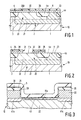
- a method of manufacturing a semiconductor device comprises providing a semiconductor body 10 having adjacent one major surface 11 a first device region 20 of one conductivity type, providing on the one major surface 11 a layer 30 doped with impurities for forming an extrinsic subsidiary region 41 of a second device region 40 of the opposite conductivity type ( Figure 8) within the first device region 20, forming an opening 31 through the doped layer 30, defining a first portion 50 of an insulating material on the side wall 32 of the doped layer 30 bounding the opening 31 and a second portion 60 of a different material on the first portion 60, and introducing through the opening 31 impurities for forming an intrinsic subsidiary region 42 of the opposite conductivity type second device region 40 within the first device region 20 and a third device region 70 of the one conductivity type within the intrinsic subsidiary region 42.
- the method comprises introducing impurities for forming a coupling subsidiary region 43 of the opposite conductivity type through the opening prior to defining the insulating first portion 50 on the side wall 32 of the doped layer 30 to form a first window 80, introducing the impurities for forming the intrinsic subsidiary region 42 of the second device region 40 through the first window 80, defining the second portion 60 on the insulating first portion 50 to form a smaller second window 90, and introducing the impurities for forming the third device region 70 through the second window 90.
- bipolar transistor which may be suitable for integration within a BiCMOS process, that is a process in which complementary n- and p- channel insulated gate field effect transistors (IGFETs) are formed together with bipolar transistors in the same semiconductor body or may be used in a purely bipolar process.
- IGFETs insulated gate field effect transistors
- the semiconductor body 10 comprises a monocrystalline silicon substrate 1 of the opposite conductivity type, in this case p- conductivity type, with a resistivity of, typically, 10 ohm-cm into which impurities of the one conductivity type (n- conductivity type in this example) are introduced using an appropriate mask to form at a device area 2 a highly doped region 21 which will later form part of the collector region 20 of the bipolar transistor.
- a layer 3 (indicated by dashed lines in the Figures) of p- conductivity type silicon with a resistivity of, typically, 8 to 12 ohm-cm is epitaxially grown on the substrate 1, thereby burying the highly doped region 21.
- a mask layer (not shown) is then defined and impurities are introduced, in this case phosphorus ions are implanted, to form an n conductivity type region 22 directly above and contacting the buried region 21.
- the region 22 forms the main subsidiary region of the collector region 20.
- the device area 2 is then defined or separated from other device areas (not shown) of the semiconductor body 10 by forming field oxide regions 4 using, for example, conventional local oxidation of silicon techniques with a silicon oxide-silicon nitride anti-oxidation mask (not shown).
- highly conductive channel stopper regions may be formed by ion implantation beneath the field oxide regions 4.
- the field oxide regions 4a, 4b serve to define a collector contact area 23 which is doped twice with impurities of the one conductivity type, once during formation of the main subsidiary region 22 of the collector region 20 and then again through an appropriate mask to form a highly doped contact region to enable ohmic contact to the collector region 20.
- a dopable layer 300 usually a semiconductor layer and, in this example a polycrystalline silicon layer, is then deposited using conventional low pressure chemical vapour deposition techniques (LPCVD).
- P conductivity type in this example boron ions, are then implanted into the polycrystalline silicon over the device area 2.
- An insulating layer 35 for example a layer of silicon dioxide, is then deposited over the device area 2.
- a conventional mask (not shown) is then defined over the insulating layer 35 and the insulating layer 35 and the doped polycrystalline silicon layer are then patterned using conventional techniques to define the doped layer 30 and to form the opening 31 thereby producing the structure shown in Figure 2.
- P conductivity type ions in this example boron ions
- boron ions are then implanted using a low dose and energy for forming the coupling region 43 of the second region 40.
- the coupling region 43 is a shallow region and, typically, boron (B+) ions with an energy of about 10keV (kilo-electron volts) and a dose of in the range of from about 1012 to about 1013 ions cm ⁇ 2 are used. The purpose of this shallow coupling region 43 will be explained below.
- a thin thermal oxide layer 33 is grown on the exposed silicon surface regions.
- An insulating layer 5 in this example a layer of tetra-ethyl-ortho-silicate (TEOS), is then deposited over the structure as shown in Figure 3.
- TEOS tetra-ethyl-ortho-silicate
- the insulating layer 5 is then etched anisotropically using conventional plasma etching (eg a CF4 or CHF3+O2 plasma) techniques to leave the insulating first portion or spacer 50 on the side wall 32 of the doped layer 30 bounding the opening 31 as shown in Figure 4.
- plasma etching eg a CF4 or CHF3+O2 plasma
- the thickness of the insulating layer 50 will be selected such that the insulating first portion or spacer 50 is about 0.2 ⁇ m wide (or thick) at its widest point, that is adjacent the exposed surface area 11a.
- a thin further insulating layer 36 for example a thermal oxide layer with a thickness of about 25nm (nanometres) is provided over the surface and, in this example, p conductivity type impurities are introduced to provide, as shown in Figure 5, a precursor region 42a for eventually forming the intrinsic subsidiary region 42 which will in this example, form the intrinsic base region of the bipolar transistor.
- a conventional masking layer (not shown) is used to mask the collector contact region 23 from this implantation.
- the p conductivity type impurities are introduced by implanting boron (B+) ions with an energy of about 35keV and a dose of in the range of about 2 to 5x10¹³ ions cm ⁇ 2.
- the p conductivity type impurities for forming the precursor region 42a may be introduced prior to forming the further insulating layer 36.
- the further insulating layer 36 may be a deposited layer, for example a TEOS layer.
- a layer 6 of undoped (that is not intentionally doped) polycrystalline material in this example a layer of undoped polycrystalline silicon of about 0.15 ⁇ m thickness, is then deposited, using conventional low pressure chemical vapour deposition techniques, over the thin further insulating layer 36.
- the polycrystalline silicon layer 6 is then etched using an anisotropic process, for example a chlorine plasma etching process, which etches polycrystalline silicon with high selectivity with respect to insulating material such as, in this example, a thermal oxide or TEOS.
- This anisotropic etching of the undoped polycrystalline silicon layer 6 results in a small, for example 0.1 ⁇ m for the emitter dimensions given above, undoped polycrystalline silicon spacer which forms the second portion 60 on the first portion 50 as shown in Figure 6.
- the thin further insulating layer 36 masks the semiconductor surface region 11a from the etchant used to etch the polycrystalline silicon layer 6 enabling the polycrystalline silicon layer 6 to be etched with high selectivity whilst avoiding erosion by the etchant of the silicon surface region 11a.
- the remaining portion of the insulating layer 36 provides a barrier beneath the polycrystalline silicon second portion 60 to prevent diffusion of the p type impurities out of the semiconductor body into the polycrystalline silicon second portion 60.
- the undoped polycrystalline silicon second insulating portion 60 thus defines the second smaller window 90 through which n-conductivity type impurities may be introduced to form the third device, in this case the emitter, region 70.
- the thin further insulating layer 36 covering the surface area 11a is then removed leaving only the portion 36a beneath the polycrystalline silicon second insulating portion 60.
- the thin further insulating 36 can be etched with a high selectivity relative to the silicon surface region 11a, for example by using a plasma etching process such as that used to form the first portion 50, so that erosion of the surface region 11a and thus loss of impurities introduced to form the intrinsic subsidiary region 42 is avoided or at least reduced.
- As+ arsenic
- the semiconductor body is heated, for example to about 925 o C (degrees Celsius) for about 60 minutes in a nitrogen atmosphere, to cause n conductivity type impurities to diffuse out of the doped layer 7 into the semiconductor body 1 to form the third, that is in this example the emitter, region 70.
- This heating treatment also drives in the previously introduced impurities so as to form the extrinsic and intrinsic subsidiary regions 41 and 42 of the second device, that is in this example the base, region 40.
- the impurities for forming the emitter region 70 could simply be implanted.
- the remaining portion of the thin further insulating layer 36a beneath the polycrystalline silicon second portion 60 serves to prevent or inhibit impurities in the doped layer 7 (or impurities being implanted to form the emitter region 70) passing through the second portion 60 into the semiconductor body 1.
- the shallow coupling region 43 is more shallow and lowly doped than the intrinsic subsidiary region 42 and is overdoped by the n conductivity type impurities introduced for forming the emitter region 70. However, outside the area of the emitter region 70, the coupling region 43 serves to ensure that there is a good low resistance coupling between the extrinsic and intrinsic subsidiary regions 41 and 42.
- the coupling region 43 thus enables the extrinsic subsidiary region 41 to be well spaced from the emitter region 70 so as to reduce leakage currents and the possibility of parasitic bipolar action whilst avoiding or at least inhibiting the possibility of punch-through between the emitter and collector regions 70 and 20.
- a further masking layer (not shown) is applied to allow the opening of contact holes for enabling a first level of metallisation, for example a layer of titanium-tungsten alloy followed by a layer of silicon-containing aluminium, to be deposited and patterned by conventional techniques to form collector, base and emitter contact electrodes C,B and E as shown in Figure 8.
- a silicide for example a cobalt or titanium silicide, layer may be formed in conventional self-aligned manner on the exposed silicon surfaces before deposition of the metallisation.
- the impurities for forming the intrinsic base region 42 are introduced through the first window 80 defined by the insulating first portion 50 whilst the impurities for forming the emitter region are introduced through the second smaller window 90 defined by the second portion 60 which is formed by an etching process which is selective with respect to the insulating first portion 50.
- This enables the emitter region 70 to be well spaced from the extrinsic base region 41 so as to inhibit hot carrier effects.
- the width (that is, by convention, the depth into the semiconductor body in the case of the intrinsic base region of a bipolar transistor) of the intrinsic subsidiary region 42 can be controlled more accurately and is less susceptible to over-etching of the oxide forming the insulating first portion 50.
- the control of the separation of the intrinsic base and emitter regions which this allows enables the current amplification (hfe) to be much less dependent on the width (that is, by convention, the dimension parallel to the one major surface 11) of the emitter region so that the current amplification is not significantly degraded by reduction in the device dimensions.
- a bipolar transistor having a measured emitter width of about 0.4 ⁇ m has a current amplification which is not significantly degraded with respect to that of a bipolar transistor having an emitter width of about 10 ⁇ m manufactured using the same method.
- the first and second portions 50 and 60 are formed of silicon oxide (TEOS) and undoped polycrystalline silicon (which in the present context is considered to be insulating), respectively, other materials could be used, provided that the material used to form the second portion 60 can be etched selectively with respect to the material of the insulating first portion 50.
- the first portion 50 may be a silicon oxide portion whilst the second portion 60 is a silicon nitride portion. If a material is available for forming the second portion 60 which can be easily etched with high selectivity relative to the first portion 50 and the semiconductor body then the further insulating layer 36 could, if desired, be omitted.
- the second portion 60 may be formed of a semiconductor or even conductive material, for example a doped polycrystalline silicon. Also, dopable materials other than polycrystalline silicon, for example amorphous silicon, may be used for the doped layer 31 and layer 7.
- a method embodying the invention may be applied to bipolar transistors which are not symmetrical about the emitter region 70, that is, for example, where the base contact B is provided on only one side of the emitter region and to lateral bipolar transistors in addition to the vertical type of bipolar transistor shown in Figure 8. Also, a method embodying the invention may be applied to other types of semiconductor devices.
- the conductivity types given above could be reversed and a method embodying the invention may be applied where the semiconductor body 1 is formed of a material other than silicon, for example a III-V material such as gallium arsenide.
Landscapes
- Bipolar Transistors (AREA)
Applications Claiming Priority (2)
| Application Number | Priority Date | Filing Date | Title |
|---|---|---|---|
| GB8921262A GB2236901A (en) | 1989-09-20 | 1989-09-20 | A method of manufacturing a semiconductor device |
| GB8921262 | 1989-09-20 |
Publications (3)
| Publication Number | Publication Date |
|---|---|
| EP0421507A2 true EP0421507A2 (de) | 1991-04-10 |
| EP0421507A3 EP0421507A3 (en) | 1991-11-06 |
| EP0421507B1 EP0421507B1 (de) | 1996-07-03 |
Family
ID=10663360
Family Applications (1)
| Application Number | Title | Priority Date | Filing Date |
|---|---|---|---|
| EP90202437A Expired - Lifetime EP0421507B1 (de) | 1989-09-20 | 1990-09-14 | Verfahren zur Herstellung eines bipolaren Transistors |
Country Status (6)
| Country | Link |
|---|---|
| US (1) | US5023192A (de) |
| EP (1) | EP0421507B1 (de) |
| JP (1) | JPH0727915B2 (de) |
| KR (1) | KR910007162A (de) |
| DE (1) | DE69027644T2 (de) |
| GB (1) | GB2236901A (de) |
Cited By (1)
| Publication number | Priority date | Publication date | Assignee | Title |
|---|---|---|---|---|
| FR2776828A1 (fr) * | 1998-03-31 | 1999-10-01 | Sgs Thomson Microelectronics | Region de base-emetteur d'un transistor bipolaire submicronique |
Families Citing this family (13)
| Publication number | Priority date | Publication date | Assignee | Title |
|---|---|---|---|---|
| US5227317A (en) * | 1989-04-21 | 1993-07-13 | Hitachi, Ltd. | Method of manufacturing semiconductor integrated circuit bipolar transistor device |
| JPH05226352A (ja) * | 1992-02-17 | 1993-09-03 | Mitsubishi Electric Corp | 半導体装置及びその製造方法 |
| WO1994016461A1 (en) * | 1993-01-04 | 1994-07-21 | Vlsi Technology, Inc. | Cmos locos isolation for self-aligned npn bjt in a bicmos process |
| JP2606648B2 (ja) * | 1993-03-19 | 1997-05-07 | 日本電気株式会社 | バイポーラトランジスタ及びその製造方法 |
| US5444003A (en) * | 1993-06-23 | 1995-08-22 | Vlsi Technology, Inc. | Method and structure for creating a self-aligned bicmos-compatible bipolar transistor with a laterally graded emitter structure |
| US5866462A (en) * | 1995-09-29 | 1999-02-02 | Analog Devices, Incorporated | Double-spacer technique for forming a bipolar transistor with a very narrow emitter |
| KR100245813B1 (ko) * | 1997-05-28 | 2000-03-02 | 윤종용 | 자기정합형 더블 폴리실리콘 바이폴라 트랜지스터및 그의 제조방법 |
| KR100486265B1 (ko) * | 2002-09-19 | 2005-05-03 | 삼성전자주식회사 | 바이폴라 트랜지스터 및 그 제조 방법 |
| DE602005023125D1 (de) | 2005-04-27 | 2010-10-07 | St Microelectronics Srl | Vertikaler MOSFET Transistor als Auswahltransistor für nichtflüchtige Speichereinrichtung betrieben |
| TWI383502B (zh) * | 2007-10-02 | 2013-01-21 | Chunghwa Picture Tubes Ltd | 畫素結構及其製造方法 |
| CN101409262B (zh) * | 2007-10-10 | 2010-06-09 | 中华映管股份有限公司 | 像素结构的制造方法 |
| US8765607B2 (en) * | 2011-06-01 | 2014-07-01 | Freescale Semiconductor, Inc. | Active tiling placement for improved latch-up immunity |
| US10032868B2 (en) * | 2016-09-09 | 2018-07-24 | Texas Instruments Incorporated | High performance super-beta NPN (SBNPN) |
Family Cites Families (13)
| Publication number | Priority date | Publication date | Assignee | Title |
|---|---|---|---|---|
| FR2508704B1 (fr) * | 1981-06-26 | 1985-06-07 | Thomson Csf | Procede de fabrication de transistors bipolaires integres de tres petites dimensions |
| US4483726A (en) * | 1981-06-30 | 1984-11-20 | International Business Machines Corporation | Double self-aligned fabrication process for making a bipolar transistor structure having a small polysilicon-to-extrinsic base contact area |
| DE3330895A1 (de) * | 1983-08-26 | 1985-03-14 | Siemens AG, 1000 Berlin und 8000 München | Verfahren zum herstellen von bipolartransistorstrukturen mit selbstjustierten emitter- und basisbereichen fuer hoechstfrequenzschaltungen |
| JPS6081862A (ja) * | 1983-10-12 | 1985-05-09 | Nippon Telegr & Teleph Corp <Ntt> | 半導体装置およびその製造方法 |
| NL8402856A (nl) * | 1984-09-18 | 1986-04-16 | Philips Nv | Werkwijze voor het vervaardigen van een halfgeleiderinrichting. |
| US4610730A (en) * | 1984-12-20 | 1986-09-09 | Trw Inc. | Fabrication process for bipolar devices |
| JPH0658912B2 (ja) * | 1985-05-07 | 1994-08-03 | 日本電信電話株式会社 | バイポーラトランジスタの製造方法 |
| EP0246682A1 (de) * | 1986-04-23 | 1987-11-25 | Koninklijke Philips Electronics N.V. | Verfahren zur Herstellung einer Halbleiteranordnung mit einer Elektrode aus polykristallinem Silizium |
| JPS63111667A (ja) * | 1986-10-29 | 1988-05-16 | Mitsubishi Electric Corp | 半導体装置の製造方法 |
| JP2565159B2 (ja) * | 1987-03-28 | 1996-12-18 | ソニー株式会社 | 半導体装置及びその製造方法 |
| US4772566A (en) * | 1987-07-01 | 1988-09-20 | Motorola Inc. | Single tub transistor means and method |
| JPH0616513B2 (ja) * | 1987-07-02 | 1994-03-02 | 日本電気株式会社 | Npn型バイポーラトランジスタの製造方法 |
| JPS6459955A (en) * | 1987-08-31 | 1989-03-07 | Nec Corp | Manufacture of semiconductor device |
-
1989
- 1989-09-20 GB GB8921262A patent/GB2236901A/en not_active Withdrawn
-
1990
- 1990-09-13 US US07/582,298 patent/US5023192A/en not_active Expired - Fee Related
- 1990-09-14 DE DE69027644T patent/DE69027644T2/de not_active Expired - Fee Related
- 1990-09-14 EP EP90202437A patent/EP0421507B1/de not_active Expired - Lifetime
- 1990-09-17 KR KR1019900014642A patent/KR910007162A/ko not_active Ceased
- 1990-09-18 JP JP2246363A patent/JPH0727915B2/ja not_active Expired - Lifetime
Cited By (2)
| Publication number | Priority date | Publication date | Assignee | Title |
|---|---|---|---|---|
| FR2776828A1 (fr) * | 1998-03-31 | 1999-10-01 | Sgs Thomson Microelectronics | Region de base-emetteur d'un transistor bipolaire submicronique |
| EP0949666A1 (de) * | 1998-03-31 | 1999-10-13 | STMicroelectronics SA | Basis-Emitter Gebiet von einem Submikrometer-Bipolartransistor |
Also Published As
| Publication number | Publication date |
|---|---|
| GB2236901A (en) | 1991-04-17 |
| JPH0727915B2 (ja) | 1995-03-29 |
| DE69027644T2 (de) | 1997-01-16 |
| GB8921262D0 (en) | 1989-11-08 |
| US5023192A (en) | 1991-06-11 |
| DE69027644D1 (de) | 1996-08-08 |
| JPH03112136A (ja) | 1991-05-13 |
| EP0421507B1 (de) | 1996-07-03 |
| EP0421507A3 (en) | 1991-11-06 |
| KR910007162A (ko) | 1991-04-30 |
Similar Documents
| Publication | Publication Date | Title |
|---|---|---|
| EP0088922B1 (de) | Verfahren zum Herstellen von Elektroden und Verdrahtungsstreifen auf einer Halbleiteranordnung | |
| EP0483487B1 (de) | Transistor mit selbstjustierender epitaxialer Basis und dessen Herstellungsverfahren | |
| US5714393A (en) | Diode-connected semiconductor device and method of manufacture | |
| US4988632A (en) | Bipolar process using selective silicon deposition | |
| US4477965A (en) | Process for manufacturing a monolithic integrated solid-state circuit comprising at least one bipolar planar transistor | |
| EP0421507B1 (de) | Verfahren zur Herstellung eines bipolaren Transistors | |
| WO1988003329A1 (en) | Process for forming mos integrated circuit devices | |
| US5194926A (en) | Semiconductor device having an inverse-T bipolar transistor | |
| US4853342A (en) | Method of manufacturing semiconductor integrated circuit device having transistor | |
| KR950010287B1 (ko) | 베이스 재결합 전류가 낮은 바이폴라 트랜지스터를 갖는 바이폴라 상보형 금속 산화물 반도체 제조 방법 | |
| US4674173A (en) | Method for fabricating bipolar transistor | |
| EP0258147A2 (de) | Verfahren zum Herstellen eines bipolaren Transistors mit einem Streifen aus Polysilizium | |
| EP0281235A1 (de) | Verfahren zum Herstellen eines bipolaren Transistors unter Verwendung von CMOS-Techniken | |
| EP0066280B1 (de) | Verfahren zur Herstellung einer Halbleitervorrichtung | |
| WO1984000850A1 (en) | Integrated circuit contact fabrication process | |
| US5882976A (en) | Method of fabricating a self-aligned double polysilicon NPN transistor with poly etch stop | |
| US5449627A (en) | Lateral bipolar transistor and FET compatible process for making it | |
| US5571731A (en) | Procedure for the manufacture of bipolar transistors without epitaxy and with fully implanted base and collector regions which are self-positioning relative to each other | |
| US5747374A (en) | Methods of fabricating bipolar transistors having separately formed intrinsic base and link-up regions | |
| US4981806A (en) | Method of manufacturing a semiconductor device | |
| US5151382A (en) | Method of manufacturing a semiconductor device by maskless pn junction isolation means | |
| JP2718257B2 (ja) | 集積回路における埋込み層容量の減少 | |
| EP0403009B1 (de) | Verfahren zur Herstellung eines Halbleiter-Bauelements | |
| EP0146760B1 (de) | Verfahren zur Herstellung eines Substratkontakts für integrierte Schaltung mittels eines Markierungsschritts | |
| US20020013025A1 (en) | Method for fabricating bipolar transistors |
Legal Events
| Date | Code | Title | Description |
|---|---|---|---|
| PUAI | Public reference made under article 153(3) epc to a published international application that has entered the european phase |
Free format text: ORIGINAL CODE: 0009012 |
|
| AK | Designated contracting states |
Kind code of ref document: A2 Designated state(s): DE FR GB IT NL |
|
| PUAL | Search report despatched |
Free format text: ORIGINAL CODE: 0009013 |
|
| AK | Designated contracting states |
Kind code of ref document: A3 Designated state(s): DE FR GB IT NL |
|
| 17P | Request for examination filed |
Effective date: 19920505 |
|
| 17Q | First examination report despatched |
Effective date: 19940331 |
|
| GRAH | Despatch of communication of intention to grant a patent |
Free format text: ORIGINAL CODE: EPIDOS IGRA |
|
| GRAH | Despatch of communication of intention to grant a patent |
Free format text: ORIGINAL CODE: EPIDOS IGRA |
|
| GRAA | (expected) grant |
Free format text: ORIGINAL CODE: 0009210 |
|
| AK | Designated contracting states |
Kind code of ref document: B1 Designated state(s): DE FR GB IT NL |
|
| PG25 | Lapsed in a contracting state [announced via postgrant information from national office to epo] |
Ref country code: NL Free format text: LAPSE BECAUSE OF FAILURE TO SUBMIT A TRANSLATION OF THE DESCRIPTION OR TO PAY THE FEE WITHIN THE PRESCRIBED TIME-LIMIT Effective date: 19960703 |
|
| REF | Corresponds to: |
Ref document number: 69027644 Country of ref document: DE Date of ref document: 19960808 |
|
| ITF | It: translation for a ep patent filed | ||
| ET | Fr: translation filed | ||
| NLV1 | Nl: lapsed or annulled due to failure to fulfill the requirements of art. 29p and 29m of the patents act | ||
| PLBE | No opposition filed within time limit |
Free format text: ORIGINAL CODE: 0009261 |
|
| STAA | Information on the status of an ep patent application or granted ep patent |
Free format text: STATUS: NO OPPOSITION FILED WITHIN TIME LIMIT |
|
| PG25 | Lapsed in a contracting state [announced via postgrant information from national office to epo] |
Ref country code: DE Effective date: 19970603 |
|
| 26N | No opposition filed | ||
| PGFP | Annual fee paid to national office [announced via postgrant information from national office to epo] |
Ref country code: GB Payment date: 19970829 Year of fee payment: 8 |
|
| PGFP | Annual fee paid to national office [announced via postgrant information from national office to epo] |
Ref country code: FR Payment date: 19970923 Year of fee payment: 8 |
|
| PG25 | Lapsed in a contracting state [announced via postgrant information from national office to epo] |
Ref country code: GB Free format text: LAPSE BECAUSE OF NON-PAYMENT OF DUE FEES Effective date: 19980914 |
|
| REG | Reference to a national code |
Ref country code: FR Ref legal event code: CD |
|
| GBPC | Gb: european patent ceased through non-payment of renewal fee |
Effective date: 19980914 |
|
| PG25 | Lapsed in a contracting state [announced via postgrant information from national office to epo] |
Ref country code: FR Free format text: LAPSE BECAUSE OF NON-PAYMENT OF DUE FEES Effective date: 19990531 |
|
| REG | Reference to a national code |
Ref country code: FR Ref legal event code: ST |
|
| PG25 | Lapsed in a contracting state [announced via postgrant information from national office to epo] |
Ref country code: IT Free format text: LAPSE BECAUSE OF NON-PAYMENT OF DUE FEES;WARNING: LAPSES OF ITALIAN PATENTS WITH EFFECTIVE DATE BEFORE 2007 MAY HAVE OCCURRED AT ANY TIME BEFORE 2007. THE CORRECT EFFECTIVE DATE MAY BE DIFFERENT FROM THE ONE RECORDED. Effective date: 20050914 |