EP0421735B1 - Procédé de fabrication d'un dispositif semiconducteur - Google Patents
Procédé de fabrication d'un dispositif semiconducteur Download PDFInfo
- Publication number
- EP0421735B1 EP0421735B1 EP90310781A EP90310781A EP0421735B1 EP 0421735 B1 EP0421735 B1 EP 0421735B1 EP 90310781 A EP90310781 A EP 90310781A EP 90310781 A EP90310781 A EP 90310781A EP 0421735 B1 EP0421735 B1 EP 0421735B1
- Authority
- EP
- European Patent Office
- Prior art keywords
- layer
- copper
- wiring layer
- metal
- thin layer
- Prior art date
- Legal status (The legal status is an assumption and is not a legal conclusion. Google has not performed a legal analysis and makes no representation as to the accuracy of the status listed.)
- Expired - Lifetime
Links
Images



Classifications
-
- H—ELECTRICITY
- H10—SEMICONDUCTOR DEVICES; ELECTRIC SOLID-STATE DEVICES NOT OTHERWISE PROVIDED FOR
- H10W—GENERIC PACKAGES, INTERCONNECTIONS, CONNECTORS OR OTHER CONSTRUCTIONAL DETAILS OF DEVICES COVERED BY CLASS H10
- H10W20/00—Interconnections in chips, wafers or substrates
- H10W20/40—Interconnections external to wafers or substrates, e.g. back-end-of-line [BEOL] metallisations or vias connecting to gate electrodes
- H10W20/41—Interconnections external to wafers or substrates, e.g. back-end-of-line [BEOL] metallisations or vias connecting to gate electrodes characterised by their conductive parts
- H10W20/44—Conductive materials thereof
- H10W20/4403—Conductive materials thereof based on metals, e.g. alloys, metal silicides
- H10W20/4421—Conductive materials thereof based on metals, e.g. alloys, metal silicides the principal metal being copper
- H10W20/4424—Copper alloys
-
- H—ELECTRICITY
- H10—SEMICONDUCTOR DEVICES; ELECTRIC SOLID-STATE DEVICES NOT OTHERWISE PROVIDED FOR
- H10P—GENERIC PROCESSES OR APPARATUS FOR THE MANUFACTURE OR TREATMENT OF DEVICES COVERED BY CLASS H10
- H10P14/00—Formation of materials, e.g. in the shape of layers or pillars
- H10P14/40—Formation of materials, e.g. in the shape of layers or pillars of conductive or resistive materials
- H10P14/412—Deposition of metallic or metal-silicide materials
-
- H—ELECTRICITY
- H10—SEMICONDUCTOR DEVICES; ELECTRIC SOLID-STATE DEVICES NOT OTHERWISE PROVIDED FOR
- H10W—GENERIC PACKAGES, INTERCONNECTIONS, CONNECTORS OR OTHER CONSTRUCTIONAL DETAILS OF DEVICES COVERED BY CLASS H10
- H10W20/00—Interconnections in chips, wafers or substrates
- H10W20/01—Manufacture or treatment
- H10W20/031—Manufacture or treatment of conductive parts of the interconnections
- H10W20/064—Manufacture or treatment of conductive parts of the interconnections by modifying the conductivity of conductive parts, e.g. by alloying
-
- H—ELECTRICITY
- H10—SEMICONDUCTOR DEVICES; ELECTRIC SOLID-STATE DEVICES NOT OTHERWISE PROVIDED FOR
- H10W—GENERIC PACKAGES, INTERCONNECTIONS, CONNECTORS OR OTHER CONSTRUCTIONAL DETAILS OF DEVICES COVERED BY CLASS H10
- H10W20/00—Interconnections in chips, wafers or substrates
- H10W20/40—Interconnections external to wafers or substrates, e.g. back-end-of-line [BEOL] metallisations or vias connecting to gate electrodes
- H10W20/41—Interconnections external to wafers or substrates, e.g. back-end-of-line [BEOL] metallisations or vias connecting to gate electrodes characterised by their conductive parts
- H10W20/425—Barrier, adhesion or liner layers
-
- H—ELECTRICITY
- H10—SEMICONDUCTOR DEVICES; ELECTRIC SOLID-STATE DEVICES NOT OTHERWISE PROVIDED FOR
- H10W—GENERIC PACKAGES, INTERCONNECTIONS, CONNECTORS OR OTHER CONSTRUCTIONAL DETAILS OF DEVICES COVERED BY CLASS H10
- H10W20/00—Interconnections in chips, wafers or substrates
- H10W20/40—Interconnections external to wafers or substrates, e.g. back-end-of-line [BEOL] metallisations or vias connecting to gate electrodes
- H10W20/45—Interconnections external to wafers or substrates, e.g. back-end-of-line [BEOL] metallisations or vias connecting to gate electrodes characterised by their insulating parts
- H10W20/47—Interconnections external to wafers or substrates, e.g. back-end-of-line [BEOL] metallisations or vias connecting to gate electrodes characterised by their insulating parts comprising two or more dielectric layers having different properties, e.g. different dielectric constants
-
- H—ELECTRICITY
- H10—SEMICONDUCTOR DEVICES; ELECTRIC SOLID-STATE DEVICES NOT OTHERWISE PROVIDED FOR
- H10W—GENERIC PACKAGES, INTERCONNECTIONS, CONNECTORS OR OTHER CONSTRUCTIONAL DETAILS OF DEVICES COVERED BY CLASS H10
- H10W20/00—Interconnections in chips, wafers or substrates
- H10W20/40—Interconnections external to wafers or substrates, e.g. back-end-of-line [BEOL] metallisations or vias connecting to gate electrodes
- H10W20/45—Interconnections external to wafers or substrates, e.g. back-end-of-line [BEOL] metallisations or vias connecting to gate electrodes characterised by their insulating parts
- H10W20/48—Insulating materials thereof
-
- Y—GENERAL TAGGING OF NEW TECHNOLOGICAL DEVELOPMENTS; GENERAL TAGGING OF CROSS-SECTIONAL TECHNOLOGIES SPANNING OVER SEVERAL SECTIONS OF THE IPC; TECHNICAL SUBJECTS COVERED BY FORMER USPC CROSS-REFERENCE ART COLLECTIONS [XRACs] AND DIGESTS
- Y10—TECHNICAL SUBJECTS COVERED BY FORMER USPC
- Y10S—TECHNICAL SUBJECTS COVERED BY FORMER USPC CROSS-REFERENCE ART COLLECTIONS [XRACs] AND DIGESTS
- Y10S148/00—Metal treatment
- Y10S148/035—Diffusion through a layer
Definitions
- the present invention relates to a semiconductor device and a method of manufacturing the same and, more particularly, to a semiconductor device having an improved wiring layer mainly made of copper and a method of manufacturing the same.
- the and thickness of wiring layers are decreased, and a multi-layered structure has been developed.
- a wiring material an aluminum alloy having a low specific resistance of 2.75 ⁇ cm and mainly made of corrosion-resistant aluminum protected form corrosion by a passivation film.
- the wiring layer made of an aluminum alloy since a current density is increased in accordance with a decrease in sectional area of the wiring, the wiring layer may be disconnected due to electromigration.
- complicated thermal hysteresis is applied to the wiring layers, and the wiring layers are disconnected by stress migration due to thermal stress acting on the wiring layers.
- the above problems are caused by the following reason. Since the melting point of aluminum is low, i.e., a temperature of 660°C, the diffusion of aluminum atoms, especially, atomic diffusion using a grain boundary as a path is accelerated even at a relatively low temperature.
- a wiring layer made of copper having a melting point higher than that of aluminum by 400°C or more has been studied.
- electromigration disconnection can be suppressed compared with an aluminum-silicon-copper (Al-Si-Cu) alloy.
- Al-Si-Cu aluminum-silicon-copper
- the service life of the copper wiring layer is improved by only several times or several tens of times compared with the aluminum alloy wiring layer. This service life almost corresponds to a service life estimated by activation energy of grain boundaries diffusion of copper atoms.
- a copper film having a thickness of about 1 ⁇ m formed by a conventional sputter film forming method has an average crystal grain size of about 1 ⁇ m.
- the width of the wiring layer In order to form a copper wiring layer having a so-called bamboo structure which has an electromigration resistance, the width of the wiring layer must be 0.5 ⁇ m or less. When the width of the wiring layer is 0.5 ⁇ m or less to improve the electromigration resistance, a practical sectional area of the wiring layer is decreased to increase its resistance. Therefore, signal transmission is delayed, and a high-speed operation is obstructed.
- the thickness of the wiring layer is increased.
- a capacitance between the adjacent wiring layers is increased to easily cause crosstalk, thereby obstructing a high-speed operation.
- K. Hoshino et al. read a method of forming an improved copper wiring layer in the VMIC Conference, p226 to p232, June 12-3 1989.
- an oxide film having a thickness of about 0.4 ⁇ m is formed on the surface of a silicon substrate, and a tungsten layer serving as an adhesion layer and a TiN layer serving as a barrier layer are sequentially deposited on the oxide film.
- a Cu-Ti alloy thin film is deposited on the TiN layer by sputter evaporation using a target made of copper and titanium. After the thin film is patterned, the thin film is heat-treated in a nitrogen atmosphere.
- a method of manufacturing a semiconductor device comprising the steps of:
- a method of manufacturing of a semiconductor device comprising a semiconductor substrate on which an element is formed, an insulating interlayer formed on the semiconductor substrate, a wiring layer formed on the insulating interlayer and having a structure in which a copper layer surface in a crystal state is covered with a nitride of a metal not forming an intermetallic compound with copper and the metal and/or the metal nitride is present at grain boundaries of the copper layer.
- the semiconductor substrate for example, a p-type silicon substrate, an n-type silicon substrate, and a silicon substrate of one conductivity type (e.g., p-type) on which n-type and p-type regions are two-dimensionally formed are used.
- the semiconductor substrate another semiconductor such as Ge, GaAs, InP, an SOS wafer obtained by forming a semiconductor layer on an insulating substrate, or an SOI wafer obtained by sequentially forming an insulating layer and semiconductor layer on a silicon substrate may be used.
- the insulating interlayer e.g., a CVD-SiO 2 single layer, or a two-layered film obtained by stacking glass film such as a phosphosilicate glass (PSG) film, a borosilicate glass (BSG), or a borophosphosilicate glass (BPSG) film on the CVD-SiO 2 film can be used.
- a phosphosilicate glass (PSG) film, a borosilicate glass (BSG), or a borophosphosilicate glass (BPSG) film on the CVD-SiO 2 film
- the BPSG film or the like on the upper surface is reflowed to prevent transfer of the step difference on the surface of the insulating interlayer to form an insulating interlayer having a flat surface.
- At least any one metal is selected from the group consisting of vanadium, niobium, tantalum, chromium, molybdenum, and tungsten.
- the thickness of the wiring layer is preferably 0.1 to 0.9 ⁇ m because of the following reason. As a grain size of copper layer constituting the wiring layer becomes large, electromigration resistance is improved. Therefore, when the thickness of the wiring layer is less than 0.1 ⁇ m, the grain size is limited by the thickness, and the electromigration resistance may not be improved. Contrast to this, when the thickness of the wiring layer exceeds 0.9 ⁇ m, a capacitance between adjacent wiring layers is increased to cause a signal transmission delay due to crosstalk. As a wiring layer for an LSI, reliability is degraded.
- a thin layer made of a metal not forming an intermetallic compound with the copper can be formed between the insulating interlayer and the wiring layer.
- the metal thin layer effectively contributes to improvement of adhesion strength of the wiring layer on the insulating interlayer.
- the metal thin layer is preferably 30% or less of the thickness of the wiring layer, because of the following reason. Since the metal thin layer serves as a part of the wiring layer and as a resistance component, when the thickness exceeds 30% of the thickness of the wiring layer, a total resistance including that of the wiring layer and a metal thin layer may be increased.
- a method of manufacturing a semiconductor device comprises the steps of forming an element on a semiconductor substrate, depositing an insulating interlayer on the semiconductor substrate, sequentially depositing a thin layer made of a metal not forming an intermetallic compound with copper and a copper layer on the insulating interlayer to form a stacked layer, patterning the stacked layer, forming a wiring layer by heat treating the patterned stacked layer in a nitrogen atmosphere to diffuse the metal of the metal thin layer to a peripheral surface of the copper layer through the copper layer, the diffused metal is nitrided to cover the copper surface in a crystal state with a nitride of a metal not forming an intermetallic compound with copper, such that the metal and/or the metal nitride is present at grain boundaries of the copper layer.
- the average grain size of the copper layer is desired to have a thickness of 0.3 ⁇ m or more.
- the thickness of the copper layer is desired to fall within a range of 0.1 to 0.8 ⁇ m such that a final wiring layer has the above thickness.
- the thickness of the metal thin layer is desired to fall within a range of a thickness which can form a monlayer of the copper atom to 30% of the thickness of the copper layer.
- the metal thin layer may be entirely diffused through the copper layer in the above heat treatment in the nitrogen atmosphere, or the metal thin layer may be partially diffused to leave part of the metal thin layer.
- a gas containing at least nitrogen gas may be used.
- a gas containing only nitrogen gas, a gas mixture of nitrogen and hydrogen gases, or a gas mixture of nitrogen and inert gases is desirably used.
- heat treatment in the nitrogen atmosphere for example, a heat treatment in a furnace filled with nitrogen gas or plasma nitriding can be used.
- a metal of the metal thin layer must be diffused on a peripheral surface of the copper layer through the copper layer, and the metal diffused in the surface must be set at a nitriding temperature.
- a heat treatment is desired to be performed at a temperature falling within a range of 600 to 750°C; a chromium thin layer, a temperature of 600 to 750°C; a vanadium thin layer, a temperature of 500 to 750°C; a tantalum thin layer, a temperature of 550 to 750°C; a molybdenum thin layer, a temperature of 700 to 750°C; and tungsten thin layer, a temperature of 700 to 750°C.
- plasma nitriding is employed as a heat treatment in the nitrogen atmosphere, the heat treatment can be performed at a temperature lower than the above temperatures.
- the grain size of the copper layer can be controlled. For example, when a heating rate is increased, the grain size of the copper layer is increased compared with not only a grain size during deposition but also the grain size in the heat treatment at a lower rate of elevating temperature.
- a heat treatment is performed in an inert atmosphere prior to the heat treatment in the nitrogen atmosphere.
- a gas containing an inert gas a gas containing only an inert gas such as argon or helium gas or a gas mixture of the inert gases and hydrogen gas is used.
- the heat treatment for example, rapid annealing using heat from an infrared lamp can be employed. Especially, when the rapid annealing is employed, the grain size of the copper layer can be further increased compared with the method of controlling a rate of an increase in temperature.
- a wiring layer has a structure in which an insulating interlayer of a semiconductor substrate is covered with a nitride of a metal not forming an intermetallic compound with copper on a copper layer surface in a crystal state and the metal and/or the metal nitride is present at the grain boundaries of the copper layer, oxidation of the wiring layer is prevented by the metal nitride covering the wiring layer to obtain an original low specific resistance of copper, and a high adhesion strength between the wiring layer and the insulating interlayer or passivation film deposited on the wiring layer.
- the wiring layer is wide not to have a bamboo structure in relation to an average crystal grain size, electromigration resistance can be improved by the nitride which is present at the grain boundaries of copper layer. For this reason, the wiring layer can be formed to be wide, and a signal propagation speed can be increased by the reduction in the above specific resistance.
- the adhesion strength of the wiring layer on the insulating interlayer can be improved.
- a thin layer made of a metal not forming an intermetallic compound with copper and a copper layer are sequentially deposited on an insulating interlayer of a semiconductor substrate, and the stacked layer is patterned and then heat-treated in a nitrogen atmosphere.
- a metal is diffused on a peripheral surface of the copper layer from the metal thin film through the copper layer thereabove, and the diffused metal is nitrided to cover the copper layer. This nitride is also formed at grain boundaries of the copper layer.
- a wiring layer having a structure in which the copper layer surface in a crystal state is covered with a nitride of a metal not forming an intermetallic compound with copper and the metal and/or the metal nitride is present at the grain boundaries of the copper layer can be formed on the insulating interlayer. Since the heat treatment can be performed at a temperature within a range not greater than 750°C (e.g., 450 to 600°C), the above electromigration can be suppressed such that an impurity diffusion layer formed on the semiconductor substrate in advance is not diffused deeper again. Therefore, a highly reliable high-speed semiconductor device having a low specific resistance wiring layer and suitable for shallowing diffusion layer can be easily manufactured.
- a heating rate is increased, or a heat treatment is performed in an inert atmosphere prior to the above heat treatment to increase the grain size of the copper film. Therefore, a wiring layer having further lower resistivity and further improved electromigration resistance can be formed on the insulating interlayer.
- a p-type silicon substrate 1 was selectively oxidized to form a field oxide film 2 having a thickness of, e.g., 0.5 ⁇ m.
- Thermal oxidation was performed to form a thermal oxide film on the surface of the island-like silicon substrate 1 isolated by the field oxide film 2.
- an arsenic-doped polysilicon film having a thickness of 0.2 ⁇ m was deposited, the silicon film and thermal oxide film were patterned to form a gate oxide film 3 and a gate electrode 4 on the surface of the substrate 1.
- n + -type source and drain regions 6 and 7 each having a junction depth of, e.g., 0.15 ⁇ m.
- a titanium thin layer having a thickness of 0.08 ⁇ m was deposited on the entire surface of the substrate by sputtering, as shown in Fig. 2B, a titanium thin layer contacting the source region 6, a drain region 7, and the gate electrode 4 of the silicon substrate was exposed by performing a heat treatment at a temperature of 750°C for 30 minutes, in a nitrogen atmosphere was silicidized to form a titanium silicide layer 8 as a buffer layer, and the titanium thin layers on the field oxide film 2 and the SiO 2 film 5 were removed. Thereafter, annealing was performed in a nitrogen atmosphere at a temperature of 900°C for 20 minutes. Note that a nickel thin layer may be deposited in place of the titanium thin layer, and a nickel silicide layer may be formed on the surfaces of the source region 6, the drain region 7, and the gate electrode 4 exposed by applying the same heat treatment as described above.
- the silicon substrate was set in a chamber of a magnetron sputtering apparatus, and after the chamber was evacuated to have a pressure of 2.0 ⁇ 10 -5 Pa or less, an argon gas was supplied to the chamber at a flow rate of 40 cm 3 /min. At this time, the pressure in the chamber was kept to be 3.7 ⁇ 10 -1 Pa.
- a chromium (Cr) target was sputtered by an argon plasma to deposit a chromium thin layer 13 having a thickness of 0.05 ⁇ m on the BPSG film 10, as shown in Fig. 2D.
- copper (Cu) target was sputtered to deposit a copper layer 14 having a thickness of 0.4 ⁇ m on the chromium thin layer 13.
- the deposited copper layer 14 consisted of grains having an average grain size of 0.2 ⁇ m.
- the sheet resistance of the stacked layer constituted by the chromium thin layer 13 and the copper layer 14 was 55 m ⁇ / ⁇ .
- the stacked layer was patterned using a reactive ion etching method to form a chromium-copper stacked layer pattern 15 on the BPSG film 10 including the tungsten plugs 12, as shown in Fig. 2E.
- the furnace was evacuated to a pressure of 1.3 ⁇ 10 -4 Pa.
- the furnace was heated to 650°C at a heating rate 50°C/min, and the temperature was kept for 30 minutes. Thereafter, the furnace was cooled at a cooling rate of 50°C/min.
- the grain size of the copper layer 14 was increased to 0.7 ⁇ m by a heat treatment in a nitrogen atmosphere.
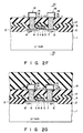
- Chromium of the chromium thin layer 13 was diffused to the peripheral surface of the copper layer 14 through crystal grain boundaries of the copper layer 14, and the diffused chromium was nitrided to form a chromium nitride (Cr 2 N or CrN) layer. At the same time, the chromium diffusing through grain boundaries of the copper layer 14 was nitrided. As a result, as shown in Figs. 2F and 3, a wiring layer 18 constituted by the copper layer 14 was formed on the remaining chromium thin layer 13.
- the peripheral surface of the layer 14 was covered with a chromium nitride layer 16 having a thickness of 0.03 ⁇ m, and the layer 14 contain chromium nitride 17 at the grain boundaries, the grains having a diameter of 0.7 ⁇ m. Thereafter, as shown in Fig. 2G, a passivation film 19 made of plasma CVD-SiO 2 having a thickness of 1.8 ⁇ m was deposited on the resultant structure, thereby manufacturing a MOS semiconductor device.
- the surface of the wiring layer 18 of a semiconductor device manufactured by the above method was covered with the chromium nitride layer 16, the surface of the wiring layer 18 was prevented from oxidation in a step of depositing the passivation film 19, and the passivation film 19 tightly contacted on the wiring layer 18.
- the chromium thin layer 13 was left under the wiring layer 18, the wiring layer 18 tightly contacted on the BPSG film 10 serving as an insulating interlayer.
- An acceleration test for supplying a current of 1 ⁇ 10 7 A/cm 2 to the wiring layer 18 was performed to the manufactured semiconductor device at a temperature of 250°C, and a disconnection time of the wiring layer 18 due to electromigration was measured. As a result, after about 100 hours from when the acceleration test was started, disconnections were detected in 50% of the wiring layer 18. Therefore, it was confirmed that the semiconductor device had excellent electromigration resistance. Note that, when the same acceleration test as described above was performed to a wiring layer made of pure copper and having the same size as in Example 1, after about 10 hours from when the acceleration test was started, disconnections were detected in 50% of the wiring layer. As described above, the wiring layer 18 formed in Example 1 had an excellent electromigration resistance, because grain size of copper layer was increased to 0.7 ⁇ m and chromium nitride was present at boundaries of crystal grains.
- the resistance was 48 m ⁇ / ⁇ . It was confirmed that the resistance could be reduced compared with the resistance (55 m ⁇ / ⁇ ) of the stacked layer pattern 15 which was not heat-treated. That is, when the resistance was converted into a specific resistance, the specific resistance could be reduced from 2.2 ⁇ cm to 1.9 ⁇ cm.
- a low specific resistance of the wiring layer can be obtained at a temperature sufficiently lower than a temperature for decreasing the number of electrically activated carrier of source and drain regions 6 and 7 formed on a silicon substrate 1 in advance.
- a gate oxide film, a gate electrode, an n + -type source region, a drain region, and a titanium silicide layer were formed on a p-type silicon substrate, and SiO 2 and BPSG films serving as an insulating interlayer are deposited.
- a contact hole was formed, and a tungsten plug was buried in the contact hole.
- a chromium layer having a thickness of 0.05 ⁇ m and a copper layer having a thickness of 0.4 ⁇ m were deposited on the BPSG film by sputtering, and a stacked layer constituted by the copper layer and the chromium thin layer was patterned to form a chromium-copper stacked layer pattern.
- the furnace was evacuated to a pressure of 1.3 ⁇ 10 -4 Pa.
- a 13.56-MHz high-frequency power of 800 W was applied to electrodes arranged on both sides of the silicon substrate in the heating furnace to generate a nitrogen plasma by RF discharge, and the silicon substrate was held in a nitrogen plasma atmosphere at a temperature of 550°C for 45 minutes. Thereafter, the RF discharge was stopped, and the silicon substrate was cooled at a cooling rate of 50°C/min.
- Example 1 a wiring layer constituted by a copper layer was formed on the remaining chromium thin layer.
- the preferal surface of the copper layer was covered with a chromium nitride layer having a thickness of 0.03 ⁇ m, and the copper layer contained chromium and/or chromium nitride at the grain boundaries, the crystal grains having a diameter of 0.7 ⁇ m.
- the resistance of the wiring layer was measured, the resistance was 48 ⁇ m/ ⁇ . It was confirmed that the resistance could be largely reduced compared with the resistance (55 m ⁇ / ⁇ ) of the stacked layer pattern which was not heat-treated. That is, when the resistance was converted into a specific resistance, the specific resistance was reduced to be 1.9 ⁇ cm compared with the specific resistance of 2.2 ⁇ cm before the heat treatment.
- Example 2 Following the same procedures as Example 1, a gate oxide film, a gate electrode, an n + -type source region, a drain region, a titanium silicide layer were formed on a p-type silicon substrate, and SiO 2 and BPSG films serving as an insulating interlayer were deposited on the resultant structure. In addition, a contact hole was formed in the resultant structure, and a tungsten plug was buried in the contact hole.
- a chromium thin layer having a thickness of 0.05 ⁇ m and a copper layer having a thickness of 0.4 ⁇ m were diposited on the BPSG film by sputtering, and a stacked layer constituted by the copper and the chromium thin layer was patterned to form a chromium-copper stacked layer pattern.
- the furnace was evacuated at a pressure of 1.3 ⁇ 10 -4 Pa.
- a wiring layer constituted by the copper layer was formed on the remaining chromium thin layer.
- the peripheral surface of the copper layer was covered with a chromium nitride layer having a thickness of 0.03 ⁇ m, and the copper layer contained chromium and/or chromium nitride at the grain boundaries, the grains having a diameter of 1.5 ⁇ m.
- the resistance of the wiring layer (including a remaining chromium thin layer) was measured, the resistance was 45 m ⁇ / ⁇ . It was confirmed that the resistance of the wiring layer could be largely reduced compared with the resistance (55 m ⁇ / ⁇ ) of the stacked layer pattern which was not thermally treated.
- the specific resistance when the resistance was converted into a specific resistance, the specific resistance could be reduced from 2.2 ⁇ cm to 1.8 ⁇ cm.
- an average grain size of copper of the wiring layer was increased to be 1.5 ⁇ m, electromigration resistance was further improved to obtain the highly reliable wiring layer.
- a gate oxide film, a gate electrode, an n + -type source region, a drain region, a titanium silicide layer were formed on a p-type silicon substrate, and SiO 2 and BPSG films serving as an insulating interlayer were deposited on the resultant structure.
- a contact hole was formed in the resultant structure, and a tungsten plug was buried in the contact hole.
- the silicon substrate was set in a chamber of a magnetron sputtering apparatus, and the chamber was evacuated to have a pressure of 2.0 ⁇ 10 -5 Pa. An argon gas was supplied to the chamber at a rate of 40 cm 3 /min.
- the chamber was kept at a pressure of 3.7 ⁇ 10 -1 Pa.
- a niobium (Nb) target was sputtered to the substrate to deposit a niobium thin layer having a thickness of 0.05 ⁇ m on the BPSG film by an argon plasma.
- a copper (Cu) target was sputtered in the same condition as in Example 1 to deposit a copper layer having a thickness of 0.4 ⁇ m on the niobium thin layer.
- the deposited copper layer consisted of grains having an average grain size of 0.2 ⁇ m.
- the resistance of the niobium and copper stacked layer was 55 m ⁇ / ⁇ .
- the stacked layer constituted by the copper layer and the niobium thin layer was patterned to form a niobium-copper stacked layer pattern having a width of 0.7 ⁇ m.
- the furnace was evacuated to a pressure of 1.3 ⁇ 10 -4 Pa.
- the furnace was heated to have a temperature of 650°C at a heating rate of 50°C/min, and the temperature was kept for 30 minutes. Thereafter, the furnace was cooled at a cooling rate of 50°C/min.
- the grain size of the copper layer was increased to 0.7 ⁇ m by a heat treatment in a nitrogen atmosphere.
- Niobium of the niobium thin layer was diffused to the peripheral surface of the copper layer through crystal grain boundaries of the copper layer, and the diffused niobium was nitrided to form a niobium nitride (Nb 2 N or NbN) layer.
- the niobium diffusing through grain boundaries of the copper layer was nitrided.
- a wiring layer constituted by the copper layer was formed on the remaining niobium thin layer.
- the peripheral surface of the copper layer was covered with a niobium nitride layer having a thickness of 0.03 ⁇ m, and the copper film contained niobium and/or niobium nitride at the grain boundaries, the grains having a diameter of 0.7 ⁇ m.
- a passivation film made of plasma CVD-SiO 2 and having a thickness of 1.8 ⁇ m was deposited on the resultant structure, thereby manufacturing a MOS semiconductor device.
- the surface of the wiring layer of a semiconductor device manufactured by the above method was covered with the niobium nitride layer, the surface of the wiring layer was prevented from oxidation in a step of depositing the passivation film, and the passivation film tightly contacted with the wiring layer.
- the niobium thin layer was left under the wiring layer, the wiring layer tightly contacted with the BPSG film serving as an insulating interlayer.
- Example 2 The same acceleration test as in Example 1 was performed to the wiring layer of the manufactured semiconductor device, and a disconnection time of the wiring layer due to electromigration was measured. As a result, after about 100 hours from when the acceleration test was started, disconnections were detected in 50% of the wiring layer 18. Therefore, it was confirmed that the semiconductor device had an excellent electromigration resistance.
- the resistance was 48 m ⁇ / ⁇ . It was confirmed that the resistance could be reduced compared with the resistance (55 m ⁇ / ⁇ ) of the stacked layer pattern 15 which was not heat-treated. That is, when the resistance was converted into a specific resistance, the specific resistance could be reduced from 2.2 ⁇ cm to 1.9 ⁇ cm.
- a highly reliable high-speed semiconductor device including a wiring layer having a specific resistance lower than the specific resistance (3 ⁇ cm) of an Al-Si-Cu alloy and in which electromigration resistance is improved, oxidation resistance is excellent, and an adhesion strength with an insulating interlayer or a passivation film is improved.
- a heat treatment in a nitrogen atmosphere for forming the wiring layer can be performed at a temperature not greater than 750°C at which an impurity diffusion layer formed on a semiconductor substrate in advance may be diffused deeper again, thereby providing a method of easily manufacturing a highly reliable high-speed semiconductor device suitable for shallowing.
Landscapes
- Internal Circuitry In Semiconductor Integrated Circuit Devices (AREA)
Claims (6)
- Procédé de fabrication d'un dispositif semiconducteur, comprenant les étapes ci-dessous:formation d'un élément sur un substrat semiconducteur (1);dépôt d'une couche intermédiaire d'isolation (9, 10) sur le substrat semiconducteur (1);dépôt séquentiel d'une fine couche (13) composée d'un métal ne formant pas de composé intermétallique avec le cuivre, et d'une couche de cuivre (14) sur la couche intermédiaire d'isolation (10) pour former une couche empilée;configuration de la couche empilée, etformation d'une couche de câblage (18) par traitement thermique de la couche empilée configurée dans une atmosphère d'azote pour diffuser le métal de la fine couche (13) vers une surface périphérique de la couche de cuivre (14), dans un état cristallin, avec un nitrure du métal ne formant pas de composé intermétallique avec le cuivre, de sorte que le métal et/ou le nitrure métallique est présent au niveau des joints de grains du film de cuivre (14),caractérisé en ce que la fine couche (13) comprend un métal sélectionné dans le groupe constitué de vanadium, de niobium, de tantale, de chrome, de molybdène et de tungstène et en ce que le traitement thermique dans une atmosphère d'azote est exécuté en présence d'une température non supérieure à 750°C.
- Procédé selon la revendication 1, caractérisé en ce qu'après la diffusion du métal dans la couche de cuivre (14) à partir de la fine couche (13) pendant le traitement thermique, la fine couche (13) est maintenue au-dessous de la couche de câblage (18).
- Procédé selon la revendication 2, caractérisé en ce que la fine couche (13) est composée de chrome.
- Procédé selon la revendication 2, caractérisé en ce que la fine couche métallique (13) est composée de niobium.
- Procédé selon la revendication 1, caractérisé en ce que le traitement thermique dans une atmosphère d'azote est une nitruration au plasma.
- Procédé selon la revendication 1, caractérisé en ce qu'un traitement thermique dans une atmosphère de gaz inerte est réalisé avant l'exécution du traitement thermique dans une atmosphère d'azote.
Applications Claiming Priority (2)
| Application Number | Priority Date | Filing Date | Title |
|---|---|---|---|
| JP1255273A JP2839579B2 (ja) | 1989-10-02 | 1989-10-02 | 半導体装置及びその製造方法 |
| JP255273/89 | 1989-10-02 |
Publications (3)
| Publication Number | Publication Date |
|---|---|
| EP0421735A2 EP0421735A2 (fr) | 1991-04-10 |
| EP0421735A3 EP0421735A3 (en) | 1991-10-30 |
| EP0421735B1 true EP0421735B1 (fr) | 1997-03-19 |
Family
ID=17276459
Family Applications (1)
| Application Number | Title | Priority Date | Filing Date |
|---|---|---|---|
| EP90310781A Expired - Lifetime EP0421735B1 (fr) | 1989-10-02 | 1990-10-02 | Procédé de fabrication d'un dispositif semiconducteur |
Country Status (5)
| Country | Link |
|---|---|
| US (1) | US5084412A (fr) |
| EP (1) | EP0421735B1 (fr) |
| JP (1) | JP2839579B2 (fr) |
| KR (1) | KR940010520B1 (fr) |
| DE (1) | DE69030229T2 (fr) |
Cited By (1)
| Publication number | Priority date | Publication date | Assignee | Title |
|---|---|---|---|---|
| US7192494B2 (en) | 1999-03-05 | 2007-03-20 | Applied Materials, Inc. | Method and apparatus for annealing copper films |
Families Citing this family (85)
| Publication number | Priority date | Publication date | Assignee | Title |
|---|---|---|---|---|
| US5243222A (en) * | 1991-04-05 | 1993-09-07 | International Business Machines Corporation | Copper alloy metallurgies for VLSI interconnection structures |
| US5130274A (en) * | 1991-04-05 | 1992-07-14 | International Business Machines Corporation | Copper alloy metallurgies for VLSI interconnection structures |
| JPH05175191A (ja) * | 1991-10-22 | 1993-07-13 | Mitsubishi Electric Corp | 積層導電配線 |
| US5310602A (en) * | 1991-11-12 | 1994-05-10 | Cornell Research Foundation | Self-aligned process for capping copper lines |
| DE4400200C2 (de) * | 1993-01-05 | 1997-09-04 | Toshiba Kawasaki Kk | Halbleitervorrichtung mit verbesserter Verdrahtungsstruktur und Verfahren zu ihrer Herstellung |
| JPH06252088A (ja) * | 1993-02-25 | 1994-09-09 | Mitsubishi Electric Corp | 半導体装置及びその製造方法 |
| US5681779A (en) * | 1994-02-04 | 1997-10-28 | Lsi Logic Corporation | Method of doping metal layers for electromigration resistance |
| WO1995034092A1 (fr) * | 1994-06-03 | 1995-12-14 | Materials Research Corporation | Procede de nitruration de couches minces de titane |
| JP3015717B2 (ja) * | 1994-09-14 | 2000-03-06 | 三洋電機株式会社 | 半導体装置の製造方法および半導体装置 |
| US5468984A (en) * | 1994-11-02 | 1995-11-21 | Texas Instruments Incorporated | ESD protection structure using LDMOS diodes with thick copper interconnect |
| US6285082B1 (en) * | 1995-01-03 | 2001-09-04 | International Business Machines Corporation | Soft metal conductor |
| EP0760020B1 (fr) * | 1995-02-16 | 1999-11-03 | Koninklijke Philips Electronics N.V. | Dispositif a commutateur comprenant une couche de chrome et procede de depot de couches de chrome par pulverisation |
| JP2679680B2 (ja) * | 1995-04-24 | 1997-11-19 | 日本電気株式会社 | 半導体装置の製造方法 |
| US5972790A (en) * | 1995-06-09 | 1999-10-26 | Tokyo Electron Limited | Method for forming salicides |
| US6268657B1 (en) * | 1995-09-14 | 2001-07-31 | Sanyo Electric Co., Ltd. | Semiconductor devices and an insulating layer with an impurity |
| US20010048147A1 (en) * | 1995-09-14 | 2001-12-06 | Hideki Mizuhara | Semiconductor devices passivation film |
| US6825132B1 (en) | 1996-02-29 | 2004-11-30 | Sanyo Electric Co., Ltd. | Manufacturing method of semiconductor device including an insulation film on a conductive layer |
| US5744376A (en) * | 1996-04-08 | 1998-04-28 | Chartered Semiconductor Manufacturing Pte, Ltd | Method of manufacturing copper interconnect with top barrier layer |
| US6100196A (en) * | 1996-04-08 | 2000-08-08 | Chartered Semiconductor Manufacturing Ltd. | Method of making a copper interconnect with top barrier layer |
| US6429120B1 (en) * | 2000-01-18 | 2002-08-06 | Micron Technology, Inc. | Methods and apparatus for making integrated-circuit wiring from copper, silver, gold, and other metals |
| US5693563A (en) * | 1996-07-15 | 1997-12-02 | Chartered Semiconductor Manufacturing Pte Ltd. | Etch stop for copper damascene process |
| KR100383498B1 (ko) | 1996-08-30 | 2003-08-19 | 산요 덴키 가부시키가이샤 | 반도체 장치 제조방법 |
| US5801098A (en) * | 1996-09-03 | 1998-09-01 | Motorola, Inc. | Method of decreasing resistivity in an electrically conductive layer |
| JP2882380B2 (ja) * | 1996-09-05 | 1999-04-12 | 日本電気株式会社 | 半導体装置及びその製造方法 |
| US6288438B1 (en) | 1996-09-06 | 2001-09-11 | Sanyo Electric Co., Ltd. | Semiconductor device including insulation film and fabrication method thereof |
| US5946596A (en) * | 1996-10-18 | 1999-08-31 | Taiwan Semiconductor Manufacturing Co., Ltd. | Method for preventing polycide line deformation by polycide hardening |
| JP3015767B2 (ja) * | 1996-12-25 | 2000-03-06 | 三洋電機株式会社 | 半導体装置の製造方法及び半導体装置 |
| US20040222525A1 (en) * | 1997-03-14 | 2004-11-11 | Rhodes Howard E. | Advanced VLSI metallization |
| US6140237A (en) * | 1997-06-16 | 2000-10-31 | Chartered Semiconductor Manufacturing Ltd. | Damascene process for forming coplanar top surface of copper connector isolated by barrier layers in an insulating layer |
| US6276072B1 (en) | 1997-07-10 | 2001-08-21 | Applied Materials, Inc. | Method and apparatus for heating and cooling substrates |
| US6690084B1 (en) | 1997-09-26 | 2004-02-10 | Sanyo Electric Co., Ltd. | Semiconductor device including insulation film and fabrication method thereof |
| US7244677B2 (en) | 1998-02-04 | 2007-07-17 | Semitool. Inc. | Method for filling recessed micro-structures with metallization in the production of a microelectronic device |
| EP1019954B1 (fr) * | 1998-02-04 | 2013-05-15 | Applied Materials, Inc. | Procédé et appareil de recuit a basse temperature intervenant après dépot électrolytique de microstructures de cuivre destinées à un dispositif micro-electronique |
| US6632292B1 (en) * | 1998-03-13 | 2003-10-14 | Semitool, Inc. | Selective treatment of microelectronic workpiece surfaces |
| US6174810B1 (en) * | 1998-04-06 | 2001-01-16 | Motorola, Inc. | Copper interconnect structure and method of formation |
| TW392325B (en) * | 1998-05-01 | 2000-06-01 | United Microelectronics Corp | Structure of metallization and process thereof |
| US6794283B2 (en) | 1998-05-29 | 2004-09-21 | Sanyo Electric Co., Ltd. | Semiconductor device and fabrication method thereof |
| US6126761A (en) * | 1998-06-10 | 2000-10-03 | International Business Machines Corporation | Process of controlling grain growth in metal films |
| US6284656B1 (en) | 1998-08-04 | 2001-09-04 | Micron Technology, Inc. | Copper metallurgy in integrated circuits |
| US6228768B1 (en) * | 1998-11-02 | 2001-05-08 | Advanced Micro Devices, Inc. | Storage-annealing plated CU interconnects |
| JP3279532B2 (ja) * | 1998-11-06 | 2002-04-30 | 日本電気株式会社 | 半導体装置の製造方法 |
| US6164781A (en) * | 1998-11-13 | 2000-12-26 | Alliedsignal Inc. | High temperature transistor with reduced risk of electromigration and differently shaped electrodes |
| US6046097A (en) * | 1999-03-23 | 2000-04-04 | United Microelectronics Corp. | Deposition method with improved step coverage |
| CN1192426C (zh) | 1999-06-22 | 2005-03-09 | 日本电气株式会社 | 铜互连 |
| US6309964B1 (en) | 1999-07-08 | 2001-10-30 | Taiwan Semiconductor Manufacturing Company | Method for forming a copper damascene structure over tungsten plugs with improved adhesion, oxidation resistance, and diffusion barrier properties using nitridation of the tungsten plug |
| US6465376B2 (en) | 1999-08-18 | 2002-10-15 | International Business Machines Corporation | Method and structure for improving electromigration of chip interconnects |
| US7262130B1 (en) | 2000-01-18 | 2007-08-28 | Micron Technology, Inc. | Methods for making integrated-circuit wiring from copper, silver, gold, and other metals |
| US6420262B1 (en) | 2000-01-18 | 2002-07-16 | Micron Technology, Inc. | Structures and methods to enhance copper metallization |
| US7211512B1 (en) * | 2000-01-18 | 2007-05-01 | Micron Technology, Inc. | Selective electroless-plated copper metallization |
| US6376370B1 (en) * | 2000-01-18 | 2002-04-23 | Micron Technology, Inc. | Process for providing seed layers for using aluminum, copper, gold and silver metallurgy process for providing seed layers for using aluminum, copper, gold and silver metallurgy |
| TW584921B (en) * | 2000-02-18 | 2004-04-21 | Applied Materials Inc | Method and apparatus for annealing copper films |
| US6440230B1 (en) | 2000-03-03 | 2002-08-27 | Micron Technology, Inc. | Nitride layer forming method |
| AU2001247109A1 (en) * | 2000-04-27 | 2001-11-12 | Nutool, Inc. | Conductive structure for use in multi-level metallization and process |
| US6674167B1 (en) * | 2000-05-31 | 2004-01-06 | Micron Technology, Inc. | Multilevel copper interconnect with double passivation |
| US6423629B1 (en) * | 2000-05-31 | 2002-07-23 | Kie Y. Ahn | Multilevel copper interconnects with low-k dielectrics and air gaps |
| JP2002057126A (ja) * | 2000-08-10 | 2002-02-22 | Fujitsu Ltd | 半導体装置とその製造方法 |
| US6294463B1 (en) * | 2000-09-13 | 2001-09-25 | Vanguard International Semiconductor Corp. | Method for manufacturing diffusion barrier layer |
| US6554914B1 (en) * | 2001-02-02 | 2003-04-29 | Novellus Systems, Inc. | Passivation of copper in dual damascene metalization |
| US7781327B1 (en) | 2001-03-13 | 2010-08-24 | Novellus Systems, Inc. | Resputtering process for eliminating dielectric damage |
| US7186648B1 (en) | 2001-03-13 | 2007-03-06 | Novellus Systems, Inc. | Barrier first method for single damascene trench applications |
| US8043484B1 (en) | 2001-03-13 | 2011-10-25 | Novellus Systems, Inc. | Methods and apparatus for resputtering process that improves barrier coverage |
| US6764940B1 (en) | 2001-03-13 | 2004-07-20 | Novellus Systems, Inc. | Method for depositing a diffusion barrier for copper interconnect applications |
| US20030008243A1 (en) * | 2001-07-09 | 2003-01-09 | Micron Technology, Inc. | Copper electroless deposition technology for ULSI metalization |
| US6917110B2 (en) * | 2001-12-07 | 2005-07-12 | Sanyo Electric Co., Ltd. | Semiconductor device comprising an interconnect structure with a modified low dielectric insulation layer |
| US6943105B2 (en) * | 2002-01-18 | 2005-09-13 | International Business Machines Corporation | Soft metal conductor and method of making |
| US8298933B2 (en) * | 2003-04-11 | 2012-10-30 | Novellus Systems, Inc. | Conformal films on semiconductor substrates |
| US7842605B1 (en) | 2003-04-11 | 2010-11-30 | Novellus Systems, Inc. | Atomic layer profiling of diffusion barrier and metal seed layers |
| US7311810B2 (en) | 2003-04-18 | 2007-12-25 | Applied Materials, Inc. | Two position anneal chamber |
| US7220665B2 (en) * | 2003-08-05 | 2007-05-22 | Micron Technology, Inc. | H2 plasma treatment |
| KR100589490B1 (ko) * | 2003-12-30 | 2006-06-14 | 동부일렉트로닉스 주식회사 | 반도체 소자의 제조 방법 |
| DE102004021239B4 (de) * | 2004-04-30 | 2017-04-06 | Infineon Technologies Ag | Lange getemperte integrierte Schaltungsanordnungen und deren Herstellungsverfahren |
| JP4561428B2 (ja) * | 2004-07-05 | 2010-10-13 | 住友金属鉱山株式会社 | 多孔質バルブ金属薄膜、その製造方法および薄膜キャパシタ |
| JP4561293B2 (ja) * | 2004-10-08 | 2010-10-13 | 住友金属鉱山株式会社 | 薄膜キャパシタおよび薄膜抵抗を有する回路部品ならびにその製造方法 |
| DE102005052001B4 (de) * | 2005-10-31 | 2015-04-30 | Advanced Micro Devices, Inc. | Halbleiterbauelement mit einem Kontaktpfropfen auf Kupferbasis und ein Verfahren zur Herstellung desselben |
| JP4863746B2 (ja) * | 2006-03-27 | 2012-01-25 | 富士通株式会社 | 半導体装置およびその製造方法 |
| US7855147B1 (en) | 2006-06-22 | 2010-12-21 | Novellus Systems, Inc. | Methods and apparatus for engineering an interface between a diffusion barrier layer and a seed layer |
| US7645696B1 (en) | 2006-06-22 | 2010-01-12 | Novellus Systems, Inc. | Deposition of thin continuous PVD seed layers having improved adhesion to the barrier layer |
| US7510634B1 (en) | 2006-11-10 | 2009-03-31 | Novellus Systems, Inc. | Apparatus and methods for deposition and/or etch selectivity |
| US7682966B1 (en) | 2007-02-01 | 2010-03-23 | Novellus Systems, Inc. | Multistep method of depositing metal seed layers |
| US7922880B1 (en) | 2007-05-24 | 2011-04-12 | Novellus Systems, Inc. | Method and apparatus for increasing local plasma density in magnetically confined plasma |
| US7897516B1 (en) | 2007-05-24 | 2011-03-01 | Novellus Systems, Inc. | Use of ultra-high magnetic fields in resputter and plasma etching |
| US7659197B1 (en) | 2007-09-21 | 2010-02-09 | Novellus Systems, Inc. | Selective resputtering of metal seed layers |
| US8017523B1 (en) | 2008-05-16 | 2011-09-13 | Novellus Systems, Inc. | Deposition of doped copper seed layers having improved reliability |
| US8518818B2 (en) | 2011-09-16 | 2013-08-27 | Taiwan Semiconductor Manufacturing Co., Ltd. | Reverse damascene process |
| JP2013222760A (ja) * | 2012-04-13 | 2013-10-28 | Panasonic Liquid Crystal Display Co Ltd | 銅配線形成方法、表示装置の製造方法 |
Family Cites Families (5)
| Publication number | Priority date | Publication date | Assignee | Title |
|---|---|---|---|---|
| DE249127C (fr) * | ||||
| US4742014A (en) * | 1985-05-10 | 1988-05-03 | Texas Instruments Incorporated | Method of making metal contacts and interconnections for VLSI devices with copper as a primary conductor |
| DE3782904T2 (de) * | 1986-09-17 | 1993-04-08 | Fujitsu Ltd | Verfahren zur ausbildung einer kupfer enthaltenden metallisierungsschicht auf der oberflaeche eines halbleiterbauelementes. |
| EP0260906B1 (fr) * | 1986-09-17 | 1993-03-10 | Fujitsu Limited | Procédé de fabrication d'un dispositif semi-conducteur, et dispositif semi-conducteur |
| JPH02165632A (ja) * | 1988-12-20 | 1990-06-26 | Toshiba Corp | 半導体装置の製造方法 |
-
1989
- 1989-10-02 JP JP1255273A patent/JP2839579B2/ja not_active Expired - Fee Related
-
1990
- 1990-09-28 KR KR1019900015505A patent/KR940010520B1/ko not_active Expired - Fee Related
- 1990-10-01 US US07/591,374 patent/US5084412A/en not_active Expired - Lifetime
- 1990-10-02 EP EP90310781A patent/EP0421735B1/fr not_active Expired - Lifetime
- 1990-10-02 DE DE69030229T patent/DE69030229T2/de not_active Expired - Fee Related
Cited By (1)
| Publication number | Priority date | Publication date | Assignee | Title |
|---|---|---|---|---|
| US7192494B2 (en) | 1999-03-05 | 2007-03-20 | Applied Materials, Inc. | Method and apparatus for annealing copper films |
Also Published As
| Publication number | Publication date |
|---|---|
| DE69030229T2 (de) | 1997-08-14 |
| US5084412A (en) | 1992-01-28 |
| JPH03119727A (ja) | 1991-05-22 |
| KR910008793A (ko) | 1991-05-31 |
| DE69030229D1 (de) | 1997-04-24 |
| KR940010520B1 (ko) | 1994-10-24 |
| JP2839579B2 (ja) | 1998-12-16 |
| EP0421735A3 (en) | 1991-10-30 |
| EP0421735A2 (fr) | 1991-04-10 |
Similar Documents
| Publication | Publication Date | Title |
|---|---|---|
| US5084412A (en) | Method of manufacturing a semiconductor device with a copper wiring layer | |
| KR950009934B1 (ko) | 반도체 장치의 배선층 형성방법 | |
| KR960010056B1 (ko) | 반도체장치 및 그 제조 방법 | |
| US5266521A (en) | Method for forming a planarized composite metal layer in a semiconductor device | |
| US7470992B2 (en) | Barrier layer stack to prevent Ti diffusion | |
| US6511910B2 (en) | Method for manufacturing semiconductor devices | |
| US5378660A (en) | Barrier layers and aluminum contacts | |
| US6593660B2 (en) | Plasma treatment to enhance inorganic dielectric adhesion to copper | |
| US6218302B1 (en) | Method for forming a semiconductor device | |
| EP0552968B1 (fr) | Dispositif semi-conducteur comprenant une couche conductrice | |
| JP3704427B2 (ja) | 半導体装置の銅金属配線形成方法 | |
| US6016010A (en) | Voidless metallization on titanium aluminide in an interconnect | |
| KR960011865B1 (ko) | 반도체 장치의 금속층 형성방법 | |
| EP0866498B1 (fr) | Méthode de formation d'un dispositif semiconducteur comportant des contacts ou vias en Aluminium | |
| US5985751A (en) | Process for fabricating interconnection of semiconductor device | |
| US6589865B2 (en) | Low pressure, low temperature, semiconductor gap filling process | |
| KR900007147B1 (ko) | 반도체장치 및 그의 제조방법 | |
| JPH09326436A (ja) | 配線形成方法 | |
| US4981816A (en) | MO/TI Contact to silicon | |
| US6468908B1 (en) | Al-Cu alloy sputtering method with post-metal quench | |
| EP0840370B1 (fr) | Refusion d'aluminium à basse température pour métallisation multicouche | |
| JPH06181212A (ja) | 半導体装置の製造方法 | |
| US5750439A (en) | Method of making aluminum alloy wiring with less silicon nodule | |
| US6528414B1 (en) | Methods for forming wiring line structures in semiconductor devices | |
| JP3337758B2 (ja) | 半導体装置の製造方法 |
Legal Events
| Date | Code | Title | Description |
|---|---|---|---|
| PUAI | Public reference made under article 153(3) epc to a published international application that has entered the european phase |
Free format text: ORIGINAL CODE: 0009012 |
|
| 17P | Request for examination filed |
Effective date: 19901029 |
|
| AK | Designated contracting states |
Kind code of ref document: A2 Designated state(s): DE FR |
|
| PUAL | Search report despatched |
Free format text: ORIGINAL CODE: 0009013 |
|
| AK | Designated contracting states |
Kind code of ref document: A3 Designated state(s): DE FR |
|
| RHK1 | Main classification (correction) |
Ipc: H01L 23/532 |
|
| 17Q | First examination report despatched |
Effective date: 19940517 |
|
| GRAG | Despatch of communication of intention to grant |
Free format text: ORIGINAL CODE: EPIDOS AGRA |
|
| GRAH | Despatch of communication of intention to grant a patent |
Free format text: ORIGINAL CODE: EPIDOS IGRA |
|
| GRAH | Despatch of communication of intention to grant a patent |
Free format text: ORIGINAL CODE: EPIDOS IGRA |
|
| RBV | Designated contracting states (corrected) |
Designated state(s): DE |
|
| GRAA | (expected) grant |
Free format text: ORIGINAL CODE: 0009210 |
|
| RAP1 | Party data changed (applicant data changed or rights of an application transferred) |
Owner name: KABUSHIKI KAISHA TOSHIBA |
|
| AK | Designated contracting states |
Kind code of ref document: B1 Designated state(s): DE |
|
| REF | Corresponds to: |
Ref document number: 69030229 Country of ref document: DE Date of ref document: 19970424 |
|
| PLBE | No opposition filed within time limit |
Free format text: ORIGINAL CODE: 0009261 |
|
| STAA | Information on the status of an ep patent application or granted ep patent |
Free format text: STATUS: NO OPPOSITION FILED WITHIN TIME LIMIT |
|
| 26N | No opposition filed | ||
| PGFP | Annual fee paid to national office [announced via postgrant information from national office to epo] |
Ref country code: DE Payment date: 20050929 Year of fee payment: 16 |
|
| PG25 | Lapsed in a contracting state [announced via postgrant information from national office to epo] |
Ref country code: DE Free format text: LAPSE BECAUSE OF NON-PAYMENT OF DUE FEES Effective date: 20070501 |