EP0422736B1 - Spiegeleinrichtung für den Bereich der UV- und Röntgenstrahlen - Google Patents
Spiegeleinrichtung für den Bereich der UV- und Röntgenstrahlen Download PDFInfo
- Publication number
- EP0422736B1 EP0422736B1 EP90202672A EP90202672A EP0422736B1 EP 0422736 B1 EP0422736 B1 EP 0422736B1 EP 90202672 A EP90202672 A EP 90202672A EP 90202672 A EP90202672 A EP 90202672A EP 0422736 B1 EP0422736 B1 EP 0422736B1
- Authority
- EP
- European Patent Office
- Prior art keywords
- layer
- heavy
- reflectivity
- materials
- mirror
- Prior art date
- Legal status (The legal status is an assumption and is not a legal conclusion. Google has not performed a legal analysis and makes no representation as to the accuracy of the status listed.)
- Expired - Lifetime
Links
- 239000000463 material Substances 0.000 claims description 93
- 238000002310 reflectometry Methods 0.000 claims description 73
- 229910052799 carbon Inorganic materials 0.000 claims description 41
- OKTJSMMVPCPJKN-UHFFFAOYSA-N Carbon Chemical group [C] OKTJSMMVPCPJKN-UHFFFAOYSA-N 0.000 claims description 34
- 125000006850 spacer group Chemical group 0.000 claims description 30
- 238000010521 absorption reaction Methods 0.000 claims description 20
- 230000000737 periodic effect Effects 0.000 claims description 12
- 229910052580 B4C Inorganic materials 0.000 claims description 10
- INAHAJYZKVIDIZ-UHFFFAOYSA-N boron carbide Chemical compound B12B3B4C32B41 INAHAJYZKVIDIZ-UHFFFAOYSA-N 0.000 claims description 3
- 230000003287 optical effect Effects 0.000 claims description 2
- 239000010948 rhodium Substances 0.000 description 34
- RPNNPZHFJPXFQS-UHFFFAOYSA-N methane;rhodium Chemical compound C.[Rh] RPNNPZHFJPXFQS-UHFFFAOYSA-N 0.000 description 14
- MHOVAHRLVXNVSD-UHFFFAOYSA-N rhodium atom Chemical compound [Rh] MHOVAHRLVXNVSD-UHFFFAOYSA-N 0.000 description 12
- PXHVJJICTQNCMI-UHFFFAOYSA-N nickel Substances [Ni] PXHVJJICTQNCMI-UHFFFAOYSA-N 0.000 description 11
- 229910052703 rhodium Inorganic materials 0.000 description 11
- 235000019592 roughness Nutrition 0.000 description 11
- 238000004364 calculation method Methods 0.000 description 6
- 229910052721 tungsten Inorganic materials 0.000 description 6
- 238000004519 manufacturing process Methods 0.000 description 5
- 229910052759 nickel Inorganic materials 0.000 description 5
- 230000002349 favourable effect Effects 0.000 description 4
- 238000000034 method Methods 0.000 description 4
- BASFCYQUMIYNBI-UHFFFAOYSA-N platinum Chemical compound [Pt] BASFCYQUMIYNBI-UHFFFAOYSA-N 0.000 description 4
- WFKWXMTUELFFGS-UHFFFAOYSA-N tungsten Chemical compound [W] WFKWXMTUELFFGS-UHFFFAOYSA-N 0.000 description 4
- 239000010937 tungsten Substances 0.000 description 4
- ZOXJGFHDIHLPTG-UHFFFAOYSA-N Boron Chemical compound [B] ZOXJGFHDIHLPTG-UHFFFAOYSA-N 0.000 description 3
- 230000002745 absorbent Effects 0.000 description 3
- 239000002250 absorbent Substances 0.000 description 3
- 230000003416 augmentation Effects 0.000 description 3
- 229910052796 boron Inorganic materials 0.000 description 3
- 239000011651 chromium Substances 0.000 description 3
- 230000007423 decrease Effects 0.000 description 3
- 238000009304 pastoral farming Methods 0.000 description 3
- 229910052710 silicon Inorganic materials 0.000 description 3
- 229910018106 Ni—C Inorganic materials 0.000 description 2
- 238000004581 coalescence Methods 0.000 description 2
- 230000007547 defect Effects 0.000 description 2
- 230000000694 effects Effects 0.000 description 2
- 238000002474 experimental method Methods 0.000 description 2
- 230000006872 improvement Effects 0.000 description 2
- 230000005855 radiation Effects 0.000 description 2
- 238000001552 radio frequency sputter deposition Methods 0.000 description 2
- 239000010703 silicon Substances 0.000 description 2
- 239000011343 solid material Substances 0.000 description 2
- 239000000758 substrate Substances 0.000 description 2
- VYZAMTAEIAYCRO-UHFFFAOYSA-N Chromium Chemical compound [Cr] VYZAMTAEIAYCRO-UHFFFAOYSA-N 0.000 description 1
- 238000001015 X-ray lithography Methods 0.000 description 1
- MEOSMFUUJVIIKB-UHFFFAOYSA-N [W].[C] Chemical compound [W].[C] MEOSMFUUJVIIKB-UHFFFAOYSA-N 0.000 description 1
- 229910045601 alloy Inorganic materials 0.000 description 1
- 239000000956 alloy Substances 0.000 description 1
- 229910052804 chromium Inorganic materials 0.000 description 1
- 229910017052 cobalt Inorganic materials 0.000 description 1
- 239000010941 cobalt Substances 0.000 description 1
- GUTLYIVDDKVIGB-UHFFFAOYSA-N cobalt atom Chemical compound [Co] GUTLYIVDDKVIGB-UHFFFAOYSA-N 0.000 description 1
- 150000001875 compounds Chemical class 0.000 description 1
- 238000000151 deposition Methods 0.000 description 1
- 230000008021 deposition Effects 0.000 description 1
- 238000009792 diffusion process Methods 0.000 description 1
- 238000009826 distribution Methods 0.000 description 1
- 229910052732 germanium Inorganic materials 0.000 description 1
- GNPVGFCGXDBREM-UHFFFAOYSA-N germanium atom Chemical compound [Ge] GNPVGFCGXDBREM-UHFFFAOYSA-N 0.000 description 1
- 229910052737 gold Inorganic materials 0.000 description 1
- 238000009499 grossing Methods 0.000 description 1
- 229910052735 hafnium Inorganic materials 0.000 description 1
- 230000003993 interaction Effects 0.000 description 1
- 238000004573 interface analysis Methods 0.000 description 1
- 229910052741 iridium Inorganic materials 0.000 description 1
- 229910052762 osmium Inorganic materials 0.000 description 1
- SYQBFIAQOQZEGI-UHFFFAOYSA-N osmium atom Chemical compound [Os] SYQBFIAQOQZEGI-UHFFFAOYSA-N 0.000 description 1
- 229910052697 platinum Inorganic materials 0.000 description 1
- 230000008569 process Effects 0.000 description 1
- 230000003252 repetitive effect Effects 0.000 description 1
- 229910052702 rhenium Inorganic materials 0.000 description 1
- WNUPENMBHHEARK-UHFFFAOYSA-N silicon tungsten Chemical compound [Si].[W] WNUPENMBHHEARK-UHFFFAOYSA-N 0.000 description 1
- 239000007787 solid Substances 0.000 description 1
- 238000004611 spectroscopical analysis Methods 0.000 description 1
- 239000007921 spray Substances 0.000 description 1
- 238000005507 spraying Methods 0.000 description 1
- 238000004544 sputter deposition Methods 0.000 description 1
- 238000003860 storage Methods 0.000 description 1
- 230000003746 surface roughness Effects 0.000 description 1
- 229910052716 thallium Inorganic materials 0.000 description 1
- BKVIYDNLLOSFOA-UHFFFAOYSA-N thallium Chemical compound [Tl] BKVIYDNLLOSFOA-UHFFFAOYSA-N 0.000 description 1
- 230000007704 transition Effects 0.000 description 1
Images


Classifications
-
- G—PHYSICS
- G02—OPTICS
- G02B—OPTICAL ELEMENTS, SYSTEMS OR APPARATUS
- G02B5/00—Optical elements other than lenses
- G02B5/08—Mirrors
- G02B5/0816—Multilayer mirrors, i.e. having two or more reflecting layers
- G02B5/085—Multilayer mirrors, i.e. having two or more reflecting layers at least one of the reflecting layers comprising metal
- G02B5/0875—Multilayer mirrors, i.e. having two or more reflecting layers at least one of the reflecting layers comprising metal the reflecting layers comprising two or more metallic layers
-
- G—PHYSICS
- G02—OPTICS
- G02B—OPTICAL ELEMENTS, SYSTEMS OR APPARATUS
- G02B5/00—Optical elements other than lenses
- G02B5/08—Mirrors
- G02B5/0891—Ultraviolet [UV] mirrors
Definitions
- the invention relates to a device of the mirror type in the field of X-UV rays, comprising the periodic stacking on a support of a said system of superimposed layers which includes a lower layer of an element of the Mendeleeff table whose atomic number Z is high, known as the first heavy element, reflecting the wavelengths of use of the mirror, and an upper layer of an element in the Mendeleeff table with a low atomic number Z, known as a light spacer element, optically poorly absorbent to said wavelengths.
- the invention finds, for example, its application in the production of X-ray spectroscopes, microscopes or telescopes, and any apparatus requiring the production of X-ray mirrors showing coefficients of reflection as large as possible, or also in the production of monochromators, which require mirrors which also show good selectivity.
- a reflective structure in the X-ray field is already known from European patent application EP-A-0128026.
- This structure is formed from pairs of metallic and non-metallic layers. It may further include a buffer layer disposed between each layer of these pairs, and between each pair, to control the interaction of the materials, that is to say to prevent interdiffusion and to stabilize this structure.
- This buffer layer must not have any effect on the absorption coefficient of the structure.
- the buffer layer may be favorably formed of silicon or of germanium or of GeSi or other alloys capable of forming an inert buffer layer between the metallic layer and the non-metallic layer of the bilayer.
- the metallic layer of the bilayer is formed from one of the elements Hf, W, Re, Ta, Pt, Ir or Au.
- the non-metallic layer is formed either of B or of B4C.
- these two layers can be chosen from the pairs W-C, Rh-C, Ni-C, in which carbon is the spacer element, and tungsten, rhodium or nickel is the heavy reflecting element.
- the W-C couple is the best known to date.
- the thickness of the two-layer system is of the order of the operating wavelength, that is to say of a few nm in the X-ray field.
- the W-C interface has a roughness of the order of 0.4 nm, while the C-W interface is almost perfect.
- Rh-C couple is more complex. It appears that rhodium pollutes the carbon layer by diffusion, while carbon reduces the intrinsic roughness of the Rh layer. As a result, the C-Rh interface has a thickness of the order of 0.5 nm, and is followed by a layer of pure rhodium.
- Ni-C couple is the most complex. A strong interdiffusion of nickel in the carbon appears on the one hand, and on the other hand the C-Ni interface also seems to be controlled by the interdiffusion of the carbon in the nickel even after a thickness of deposit of 2 nm.
- mirrors for X-rays are produced by means of multilayers formed from the silicon-tungsten couple.
- silicon is the spacer element and tungsten is the heavy reflecting element.
- the interface roughness must be minimized.
- the materials of the couple are chosen for this purpose using coalescence as a criterion. A low coalescence thickness favors obtaining a minimum interface roughness.
- the wavelength of use of the mirror is linked to the choice of the pair of spacer element and reflecting element; in other words, for a given application, and a defined X-ray source, the selectivity and the reflectivity of the mirror are determined essentially by the choice of bilayer materials.
- the materials which constitute the best candidates for producing a mirror at a given wavelength, for a chosen application may in reality not be suitable for industrial use. satisfactory, owing to the fact that they have interface roughnesses or faults linked to the interdiffusion.
- An object of the present invention is to provide a mirror type device as defined in the preamble whose technical characteristics and whose optical properties are improved compared to those of devices formed by the periodic stacking of a two-layer system.
- an object of the invention is to provide a device whose reflectivity is improved compared to that of known devices.
- Another object of the invention is to propose a device in which the surface roughness or the interdiffusion are reduced so that these defects no longer prohibit the use of the materials best suited to the operating wavelength chosen .
- the reflectivity of the mirror is improved compared to what would be the reflectivity of a mirror formed of the same number of layer systems, the latter being made up of the best of the two pairs heavy element - light element.
- this device is characterized in that the heavy elements and the light element are such that the potential reflectivities of said couples of the three-layer system are equivalent.
- the reflectivity of the mirror is further improved.
- this device is characterized in that the heavy element of the intermediate layer is such that it has, with the heavy element of the lower layer and the light element of the upper layer, the lowest interdiffusion and minimum interface roughness.
- the performance of the mirror is as close as possible to the expected theoretical performance.
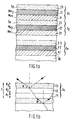
- a mirror operating in the X-UV field for example between 1 and 20nm is formed of a periodic stack of said layer systems, S1, S2, ... S n .
- Each layer system for example S1, comprises, as shown in FIG. 1b, a lower layer 11, of thickness d1 in a first heavy material, which has a high electron density, reflecting in the wavelength range ⁇ of use of the mirror, an intermediate layer 12, of thickness d2 in a second heavy material also reflecting in this range of wavelength ⁇ , and an upper layer 13 of thickness d3, in a light material designated under the spacer name.
- Heavy materials are then understood to mean materials formed from an element whose atomic number Z is high in Mendeleieff's table, and light materials are understood to mean materials formed from an element whose atomic number Z is low. Light materials will be found in particular in the first two columns of Mendeleieff's table and heavy materials in the other columns. For light materials the indices ⁇ and ⁇ of the relation (1) have low values.
- FIG. 2a the real index ⁇ , respectively of the carbon in broken lines, and of rhodium in solid lines; and in FIG. 2b, the complex index ⁇ of the carbon in broken lines respectively, and of rhodium in solid lines.
- This condition imposes very small thicknesses, of the order of a few nanometers for wavelengths of use ⁇ located in the range from 1 to 100 nm.
- Sources that require mirrors working in this wavelength range are new sources of X-UV radiation (such as synchrotrons, storage rings, etc.).
- the various fields of application are, for example, spectroscopy, X-ray lithography, X-ray telescopes etc., which require mirrors with a high reflection coefficient.
- the reflectivity and selectivity of the mirrors depend on a certain number of parameters among which we count: the choice of materials, the regularity in thickness throughout the stack, the roughness of the layers at the interfaces , and the purity of the materials.
- bilayers as known either two technologically compatible materials but forming a bilayer with low theoretical reflectivity, or two materials with high theoretical reflectivity but forming a technologically unfavorable bilayer.
- ⁇ is the complex index defined by the relation (1);
- R max is the maximum theoretical reflectivity that can be expected from a pair of given materials, as described in the state of the art, that is to say comprising a lower layer of heavy material, and a upper layer formed of carbon as a spacer;
- N opt is the theoretical optimal number of layers to obtain R max under normal incidence.
- the reflectivity of a solid material is therefore very low, that is to say of the order of 10 ⁇ 4, apart from very grazing incidences. This is why it is essential to produce the mirrors used in the wavelength range by means of multilayer systems, in order to be able to work at non-grazing angles.
- a multilayer mirror with bilayer systems already makes it possible to obtain a gain in reflectivity of around 103 compared to a mirror made of a solid material. We will seek, according to the invention, to optimize these performances.
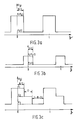
- the dielectric susceptibility ⁇ (Z) is periodic in the direction Z perpendicular to the layers.
- the profile of complex index is represented by FIG. 3c.
- the Z dependence of the dielectric susceptibility can be represented as the sum of two dependencies plotted in FIGS. 3a and 3b.
- the profile of Figure 3c is then the sum of the profiles of Figures 3a and 3b.
- the calculations are carried out on three-layer systems, completely asymmetrical, therefore mathematically more difficult to study.
- a digital simulation program was therefore used to calculate the theoretical reflectivity of a mirror composed of three-layer systems.
- the materials of the three-layer system can be characterized by two absorption contrasts ⁇ 1 and ⁇ 2 given by relations (8) and (9).
- ⁇ 1 Im ⁇ 1 Im ⁇ 3 - 1
- ⁇ 2 Im ⁇ 2 Im ⁇ 3 - 1 (9) and by two contrast ratios of real and imaginary indices T1 and T2 given by:
- T1 Re ( ⁇ 1 - ⁇ 3) Im ( ⁇ 1 - ⁇ 3) (10);
- T2 Re ( ⁇ 2 - ⁇ 3) Im ( ⁇ 2 - ⁇ 3) (11)
- the method for making this selection comprises the following series of steps:
- the person skilled in the art will first seek the light material to constitute the upper layer 13 or spacer of the three-layer system.
- This layer must be produced by means of an element from the Mendeleieff table which has a minimum of absorption for the given wavelength.
- a spacer will preferably be chosen which will comprise boron, such as for example the boron carbide B4C and which will have a minimum absorption at this wavelength.
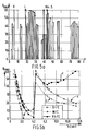
- FIG. 4a represents these maximum isoreflectivity curves R max , the absorption contrast ⁇ being plotted on the abscissa and the index contrast ratio T being plotted on the ordinate. These layers are plotted with an increment of 5%. They show that the maximum reflectivities are obtained when the Me-Sp couple has both a high contrast ratio of index T and a low absorption contrast ⁇ . They also show that the same reflectivity (for example 50%) can be obtained if the Me-Sp couple has a low contrast ratio of index T and a strong absorption contrast ⁇ .
- the first case is for example concretized by the point M2 of figure 4a, and the second case by the point M1 of this same figure.
- the point M3, also on the 50% isoreflectivity curve corresponds to intermediate values of ⁇ and T.
- Figure 4b shows the position in the plane ( ⁇ , T) of some real Me-Sp couples where the spacer is carbon, and for the wavelength of the line K ⁇ of carbon.
- T and ⁇ have mean values corresponding to Me chosen from among others nickel (Ni), cobalt (Co) etc ...
- the maximum achievable increase in reflectivity is established by stacking two heavy materials, a first heavy material Me1 for the layer 11, a second heavy material Me2 for the layer 12, and a light spacer material Sp for the layer 13 forming the three-layer system according to the invention.
- Me-Sp pair corresponds to a pair ( ⁇ , T). So at (Me1 - SP) corresponds ( ⁇ 1, T1) (Me2 - SP) corresponds ( ⁇ 2, T2)
- the determination of the increase in reflectivity is made by using on the one hand the relations (8) and (9) giving ⁇ 1 and ⁇ 2, and on the other hand the relations (10) and (11) giving T1 and T2.
- the point M1 of this example is on the line of isoreflectivity 50% with: ⁇ 1 strong T1 weak
- FIG. 6a shows lines of increase in isoreflectivity with respect to the line of isoreflectivity 50%, by considering this reflectivity as the maximum reflectivity with the best of cases using two materials. This representation is made with an increment of 1% compared to 50%, that is to say 2% compared to 100% of maximum reflectivity.
- the point M2 is on the line of isoreflectivity 50% with, in general. You strong ⁇ 2 low
- FIG. 6b shows lines of increase in isoreflectivity compared to the line of isoreflectivity 50% considering the best of cases with 2 materials. This representation is made as in FIG. 6a with an increment of 1% compared to 50%.
- Table II gives the theoretical results which can be approached by associating suitable heavy materials stacked in the right direction, with the Rh-C couple.
- a person skilled in the art is able to determine, with the aid of the teaching of the present invention, numerous three-layer systems suitable for producing mirrors multilayer of a wavelength, or in a determined wavelength range.
- FIG. 7a which represents the reflectivity (on the ordinate) as a function of the angle of incidence ⁇ that the peak obtained is wider than for a two-layer system. This is very favorable for certain applications, since the amount of integrated light is greater.
- FIGS. 8a to 8d make it possible to understand physically the origin of the increase in reflectivity in a three-layer system compared to the best of the two couples which can form a bilayer, which composes it.
- FIG. 8a shows the evolution of the energy E in a real multilayer mirror formed from tungsten-carbon bilayer systems (WC), as well as the ratio ⁇ / ⁇ 1 of the real indices of the two materials as a function of the thickness Z traversed by the light.
- Figure 8b shows the same evolution when the bilayer system is rhodium-carbon (Rh-C).
- the absorption contrast ⁇ 75 is greater in the WC system than in the Rh-C system ( ⁇ 12). It follows that the index profile is optimal when in these systems the thickness d W of the layer of W is significantly smaller than that d Rh of the layer of Rh, d ′ representing the thickness of the layer of carbon .
- FIG. 8c shows the same evolution when the system is a three-layer, in which the layers are stacked in the direction recommended by the teaching of the invention: the energy maxima are found in the reflective layer and the minima in the absorbent layer.
- Figure 8d shows the same evolution in a three-layer system in which the two heavy materials are instead stacked in "the wrong way", as the profile of the real indices that have been superimposed on the energy curve.
- the energy maxima are found outside the reflective layer and the reflectivity is considerably reduced.
- An embodiment method for forming the multilayer mirrors described above can include radio frequency sputtering (rf sputtering) of the chosen materials, on a substrate.
- RF sputtering involves applying an alternating voltage to a target in order to spray the material onto a substrate. This method makes it possible to work with very varied growth rates of layers 0.001nm / s to 10nm / s.
- the sample is placed alternately under each target, for example by rotations carried out in a few seconds.
- a flap system can cover or uncover the sample to subject it or shield it from the spraying of a material. Such a system makes it possible to control the deposition times and therefore the thicknesses with great precision.
- boron carbide C4B which has a density slightly lower than that of carbon, and therefore more advantageous potential performance near the absorption thresholds of boron and carbon.
- W tungsten
- the optimized stacking direction according to the invention is W / Rh / B4C and we observe an interesting increase in reflectivity in the range: 6.76nm ⁇ ⁇ 11.4nm
- Rh-B4C interfaces are practically ideal.
- the Rh-B4C interfaces are a little worse, but the performance of the mirror with three-layer systems is nevertheless better than that obtained with the best bilayer which is Rh / B4C.
Landscapes
- Physics & Mathematics (AREA)
- General Physics & Mathematics (AREA)
- Optics & Photonics (AREA)
- Optical Elements Other Than Lenses (AREA)
Claims (8)
- Spiegeleinrichtung für den Bereich der UV- und Röntgenstrahlen, die auf einem Träger (10) den periodischen Stapel (S₁, S₂...Sn) eines sog. Systems überlagerter Schichten enthält, das eine untere Schicht (11; 21; ...n1) eines ersten Elements der Mendeleeff-Tafel mit höherer Atomzahl Z mit der Bezeichnung des ersten Schwerelements umfaßt, das auf den Wellenlängen bei Anwendung des Spiegels reflektiert, und eine obere Schicht (13; 23; ...n3) eines Elements der Mendeleeff-Tafel mit niedrigerer Atomzahl Z mit der Bezeichnung des leichten Distanzelements umfaßt, das bei diesen Wellenlängen eine niedrige optische Absorption aufweist, dadurch gekennzeichnet, daß das System der überlagerten Schichten (11, 13) zwischen der unteren Schicht (11) und der oberen Schicht (13) eine Zwischenschicht (12) aus einem sog. zweiten schweren Element (Me₂) enthält, das auf den Anwendungswellenlängen zur Bildung eines Dreischichtensystems (11, 12, 13) retlektiert, und daß die ersten und zweiten schweren Elemente (Me₁, Me₂) der unteren (11) und Zwischenschichten (12) mit dem leichteren Distanzelement (Sp) der oberen Schicht (13) ein erstes bzw. ein zweites Paar (Me1-Sp; Me2-Sp) derart bilden, daß das erste Paar (Me1-Sp) einen höheren Absorptionskontrast α1 > α2 besitzt und ein niedrigeres Kontrastverhältnis der Indizes T₁ > T₂ als das zweite Paar (Me2-Sp) hat,- die Absorptionskontraste α1 und α2 der ersten und zweiten Paare ausgehend von imaginären Anteilen Imε₁, Imε₂ und Imε₃ der elektrischen Suszeptibilitäten ε₁, ε₂ und ε₃ durch folgende Gleichungen definiert werden
 - und die Kontrastverhältnisse der Indizes T₁ und T₂ des ersten schweren Elements, des zweiten schweren Elements bzw. des leichten Elements ausgehend von den imaginären Anteilen Imε₁, Imε₂ und Imε₃ und von den Realanteilen Reε₁, Reε₂ und Reε₃ dieser elektrischen Suszeptibilitäten durch folgende Gleichungen definiert werden:
- Spiegeleinrichtung nach Anspruch 1, dadurch gekennzeichnet, daß die schweren Elemente und das leichte Element derart beschaffen sind, daß die potentiellen Reflexionskräfte der Dreischichtensystempaare gleichwertig sind.
- Spiegeleinrichtung nach einem der Ansprüche 1 oder 2, dadurch gekenn zeichnet, daß das schwere Element der Zwischenschicht derart beschaffen ist, daß es mit dem schweren Element der oberen Schicht und mit dem leichten Element der oberen Schicht die schwächste Interdiffusion und eine minimale Grenzflächenrauheit aufweist.
- Spiegeleinrichtung nach einem oder mehreren der vorangehenden Ansprüche, dadurch gekennzeichnet, daß das leichte Element der Kohlenstoff C oder das Borkarbid B₄C ist.
- Spiegeleinrichtung nach Anspruch 4, dadurch gekennzeichnet, daß das Dreischichtensystem aus der Stapelung W-Rh-C in dieser Reihenfolge besteht.
- Spiegeleinrichtung nach Anspruch 4, dadurch gekennzeichnet, daß das Dreischichtensystem aus der Stapelung Os-Sb-C in dieser Reihenfolge besteht.
- Spiegeleinrichtung nach Anspruch 4, dadurch gekennzeichnet, daß das Dreischichtensystem aus einem der folgenden Stapel besteht:
Cr - Li - C
Ti - Cr - C
Ni - Cr - C
W - Cr - C
Pt - Cr - C
Au - Cr - C
Os - Cr - C,
wobei die Werkstoffe in dieser Reihenfolge gestapelt sind. - Spiegeleinrichtung nach Anspruch 4, dadurch gekennzeichnet, daß das Dreischichtensystem aus der Stapelung von W-Rh-B₄-C in dieser Reihenfolge besteht.
Applications Claiming Priority (2)
| Application Number | Priority Date | Filing Date | Title |
|---|---|---|---|
| FR8913423 | 1989-10-13 | ||
| FR8913423A FR2653234A1 (fr) | 1989-10-13 | 1989-10-13 | Dispositif du type miroir dans le domaine des rayons x-uv. |
Publications (2)
| Publication Number | Publication Date |
|---|---|
| EP0422736A1 EP0422736A1 (de) | 1991-04-17 |
| EP0422736B1 true EP0422736B1 (de) | 1995-01-11 |
Family
ID=9386382
Family Applications (1)
| Application Number | Title | Priority Date | Filing Date |
|---|---|---|---|
| EP90202672A Expired - Lifetime EP0422736B1 (de) | 1989-10-13 | 1990-10-08 | Spiegeleinrichtung für den Bereich der UV- und Röntgenstrahlen |
Country Status (6)
| Country | Link |
|---|---|
| US (1) | US5216539A (de) |
| EP (1) | EP0422736B1 (de) |
| JP (1) | JP2962487B2 (de) |
| DE (1) | DE69015952T2 (de) |
| FR (1) | FR2653234A1 (de) |
| WO (1) | WO1991006021A1 (de) |
Families Citing this family (39)
| Publication number | Priority date | Publication date | Assignee | Title |
|---|---|---|---|---|
| JPH075296A (ja) * | 1993-06-14 | 1995-01-10 | Canon Inc | 軟x線用多層膜 |
| BE1007607A3 (nl) * | 1993-10-08 | 1995-08-22 | Philips Electronics Nv | Multilaagspiegel met verlopende brekingsindex. |
| US5485499A (en) * | 1994-08-05 | 1996-01-16 | Moxtek, Inc. | High throughput reflectivity and resolution x-ray dispersive and reflective structures for the 100 eV to 5000 eV energy range and method of making the devices |
| DE19826259A1 (de) * | 1997-06-16 | 1998-12-17 | Bosch Gmbh Robert | Verfahren und Einrichtung zum Vakuumbeschichten eines Substrates |
| US6108131A (en) | 1998-05-14 | 2000-08-22 | Moxtek | Polarizer apparatus for producing a generally polarized beam of light |
| US7306338B2 (en) | 1999-07-28 | 2007-12-11 | Moxtek, Inc | Image projection system with a polarizing beam splitter |
| US6666556B2 (en) | 1999-07-28 | 2003-12-23 | Moxtek, Inc | Image projection system with a polarizing beam splitter |
| US6447120B2 (en) | 1999-07-28 | 2002-09-10 | Moxtex | Image projection system with a polarizing beam splitter |
| JP2001057328A (ja) * | 1999-08-18 | 2001-02-27 | Nikon Corp | 反射マスク、露光装置および集積回路の製造方法 |
| US6413268B1 (en) | 2000-08-11 | 2002-07-02 | Raymond A. Hartman | Apparatus and method for targeted UV phototherapy of skin disorders |
| US6389099B1 (en) | 2000-11-13 | 2002-05-14 | Rad Source Technologies Inc. | Irradiation system and method using X-ray and gamma-ray reflector |
| US7375887B2 (en) | 2001-03-27 | 2008-05-20 | Moxtek, Inc. | Method and apparatus for correcting a visible light beam using a wire-grid polarizer |
| DE10134266C2 (de) * | 2001-07-18 | 2003-09-18 | Geesthacht Gkss Forschung | Einrichtung und Verfahren zur Analyse atomarer und/oder molekularer Elemente mittels wellenlängendispersiver, röntgenspektrometrischer Einrichtungen |
| US7061561B2 (en) | 2002-01-07 | 2006-06-13 | Moxtek, Inc. | System for creating a patterned polarization compensator |
| US6909473B2 (en) | 2002-01-07 | 2005-06-21 | Eastman Kodak Company | Display apparatus and method |
| US6785050B2 (en) | 2002-05-09 | 2004-08-31 | Moxtek, Inc. | Corrosion resistant wire-grid polarizer and method of fabrication |
| EP1369744A1 (de) * | 2002-06-06 | 2003-12-10 | ASML Netherlands B.V. | Lithographischer Apparat und Verfahren zur Herstellung einer Vorrichtung |
| TWI227380B (en) * | 2002-06-06 | 2005-02-01 | Asml Netherlands Bv | Lithographic apparatus and device manufacturing method |
| TWI237733B (en) * | 2003-06-27 | 2005-08-11 | Asml Netherlands Bv | Laser produced plasma radiation system with foil trap |
| WO2005019881A1 (en) * | 2003-08-12 | 2005-03-03 | Massachusetts Institute Of Technology | Process for fabrication of high reflectors by reversal of layer sequence and application thereof |
| JP4566791B2 (ja) * | 2004-03-26 | 2010-10-20 | キヤノン株式会社 | 軟x線多層膜反射鏡 |
| US7800823B2 (en) | 2004-12-06 | 2010-09-21 | Moxtek, Inc. | Polarization device to polarize and further control light |
| US7570424B2 (en) * | 2004-12-06 | 2009-08-04 | Moxtek, Inc. | Multilayer wire-grid polarizer |
| US7630133B2 (en) | 2004-12-06 | 2009-12-08 | Moxtek, Inc. | Inorganic, dielectric, grid polarizer and non-zero order diffraction grating |
| US7961393B2 (en) | 2004-12-06 | 2011-06-14 | Moxtek, Inc. | Selectively absorptive wire-grid polarizer |
| JP2006258650A (ja) * | 2005-03-17 | 2006-09-28 | Nikon Corp | 多層膜反射鏡および露光装置 |
| US8755113B2 (en) | 2006-08-31 | 2014-06-17 | Moxtek, Inc. | Durable, inorganic, absorptive, ultra-violet, grid polarizer |
| US7789515B2 (en) | 2007-05-17 | 2010-09-07 | Moxtek, Inc. | Projection device with a folded optical path and wire-grid polarizer |
| US7848483B2 (en) * | 2008-03-07 | 2010-12-07 | Rigaku Innovative Technologies | Magnesium silicide-based multilayer x-ray fluorescence analyzers |
| US8248696B2 (en) | 2009-06-25 | 2012-08-21 | Moxtek, Inc. | Nano fractal diffuser |
| US8913321B2 (en) | 2010-09-21 | 2014-12-16 | Moxtek, Inc. | Fine pitch grid polarizer |
| US8611007B2 (en) | 2010-09-21 | 2013-12-17 | Moxtek, Inc. | Fine pitch wire grid polarizer |
| US8873144B2 (en) | 2011-05-17 | 2014-10-28 | Moxtek, Inc. | Wire grid polarizer with multiple functionality sections |
| US8913320B2 (en) | 2011-05-17 | 2014-12-16 | Moxtek, Inc. | Wire grid polarizer with bordered sections |
| US8922890B2 (en) | 2012-03-21 | 2014-12-30 | Moxtek, Inc. | Polarizer edge rib modification |
| US9354374B2 (en) | 2013-10-24 | 2016-05-31 | Moxtek, Inc. | Polarizer with wire pair over rib |
| WO2015161934A1 (en) * | 2014-04-23 | 2015-10-29 | Asml Netherlands B.V. | A lithographic apparatus, radiation source, and lithographic system |
| CN109637691B (zh) * | 2018-12-13 | 2020-10-30 | 中国工程物理研究院激光聚变研究中心 | 一种二值化x光选能器件及其制备方法 |
| WO2026069912A1 (ja) * | 2024-09-27 | 2026-04-02 | 株式会社島津製作所 | 軟x線・極端紫外線用回折格子 |
Family Cites Families (9)
| Publication number | Priority date | Publication date | Assignee | Title |
|---|---|---|---|---|
| US4317043A (en) * | 1979-10-26 | 1982-02-23 | The University Of Rochester | Normal incidence x-ray reflectors and resonant cavities for supporting laser action using the same |
| US4693933A (en) * | 1983-06-06 | 1987-09-15 | Ovonic Synthetic Materials Company, Inc. | X-ray dispersive and reflective structures and method of making the structures |
| US4785470A (en) * | 1983-10-31 | 1988-11-15 | Ovonic Synthetic Materials Company, Inc. | Reflectivity and resolution X-ray dispersive and reflective structures for carbon, beryllium and boron analysis |
| US4684565A (en) * | 1984-11-20 | 1987-08-04 | Exxon Research And Engineering Company | X-ray mirrors made from multi-layered material |
| JPH07113679B2 (ja) * | 1986-03-28 | 1995-12-06 | 日本電信電話株式会社 | 多層膜反射鏡 |
| US4969175A (en) * | 1986-08-15 | 1990-11-06 | Nelson Robert S | Apparatus for narrow bandwidth and multiple energy x-ray imaging |
| US4786128A (en) * | 1986-12-02 | 1988-11-22 | Quantum Diagnostics, Ltd. | Device for modulating and reflecting electromagnetic radiation employing electro-optic layer having a variable index of refraction |
| DE3856054T2 (de) * | 1987-02-18 | 1998-03-19 | Canon K.K., Tokio/Tokyo | Reflexionsmaske |
| DE68923890T2 (de) * | 1988-02-25 | 1996-02-22 | Japan Res Dev Corp | Strahlenoptische Elemente mit Graphit-Schichten. |
-
1989
- 1989-10-13 FR FR8913423A patent/FR2653234A1/fr active Pending
-
1990
- 1990-10-08 DE DE69015952T patent/DE69015952T2/de not_active Expired - Lifetime
- 1990-10-08 EP EP90202672A patent/EP0422736B1/de not_active Expired - Lifetime
- 1990-10-10 WO PCT/NL1990/000147 patent/WO1991006021A1/fr not_active Ceased
- 1990-10-10 US US07/688,621 patent/US5216539A/en not_active Expired - Lifetime
- 1990-10-10 JP JP2514297A patent/JP2962487B2/ja not_active Expired - Fee Related
Also Published As
| Publication number | Publication date |
|---|---|
| EP0422736A1 (de) | 1991-04-17 |
| WO1991006021A1 (fr) | 1991-05-02 |
| US5216539A (en) | 1993-06-01 |
| FR2653234A1 (fr) | 1991-04-19 |
| JPH04502213A (ja) | 1992-04-16 |
| DE69015952T2 (de) | 1995-08-24 |
| JP2962487B2 (ja) | 1999-10-12 |
| DE69015952D1 (de) | 1995-02-23 |
Similar Documents
| Publication | Publication Date | Title |
|---|---|---|
| EP0422736B1 (de) | Spiegeleinrichtung für den Bereich der UV- und Röntgenstrahlen | |
| EP2005245B1 (de) | Extrem-ultraviolett-fotolithographiemaske mit resonanzbarrierenschicht | |
| EP1468428B1 (de) | Optische anordnung und verfahren dazu | |
| EP0021993B1 (de) | Integrierte Fresnel-Linse | |
| Tarrio et al. | Optical constants of in situ-deposited films of important extreme-ultraviolet multilayer mirror materials | |
| EP2513688A1 (de) | Optimiertes dielektrisches reflexionsbeugungsgitter | |
| EP1700141B1 (de) | Zweidimensionales beugungsgitter mit alternierenden mehrschichtstapeln und spektroskopische einrichtung mit dem gitter | |
| EP1955110B1 (de) | Extrem-ultraviolett-fotolithografiemaske mit absorbierenden hohlräumen | |
| EP1464993B1 (de) | EUV optische Vorrichtung mit verstärkter mechanischer Stabilität und lithographische Maske mit dieser Vorrichtung | |
| FR2712990A1 (fr) | Miroir à large bande et à haute réflectivité et procédé de réalisation d'un tel miroir. | |
| US20020113974A1 (en) | System of beam narrowing for resolution enhancement and method therefor | |
| EP1842209B1 (de) | Röntgen- oder neutronen-monochromatisierer | |
| JP2014119616A (ja) | マイクロデバイス及び光偏向器並びに光学デバイス | |
| FR2658619A1 (fr) | Miroirs interferentiels multifractals de dimensions fractales entre 0 et 1. | |
| EP0534535A1 (de) | Vorrichtung mit Spiegel der in Röntgenstrahlung- oder Neutronenbereich arbeitet | |
| JPH06186403A (ja) | 多層膜光学部材 | |
| WO2007068614A1 (fr) | Masque de lithographie en reflexion et procede de fabrication du masque | |
| Hunter et al. | Thin-film interference mirror to suppress grating harmonics in vacuum-ultraviolet radiation | |
| JP2007163614A (ja) | 多層膜ミラー | |
| WO2007135183A1 (fr) | Ensemble optique de coques réflectives et procédé associé | |
| WO1997023789A1 (fr) | Rejecteur spectral grand champ angulaire et procede de fabrication | |
| JP2006308483A (ja) | 多層膜及び多層膜の製造方法 | |
| EP0369277A1 (de) | Halbreflektierende und achromatische optische Komponente | |
| US20080085414A1 (en) | Optical Substrate and Method of Manufacture | |
| FR3079035A1 (fr) | Dispositif optique pour rayons x |
Legal Events
| Date | Code | Title | Description |
|---|---|---|---|
| PUAI | Public reference made under article 153(3) epc to a published international application that has entered the european phase |
Free format text: ORIGINAL CODE: 0009012 |
|
| AK | Designated contracting states |
Kind code of ref document: A1 Designated state(s): DE FR GB NL |
|
| 17P | Request for examination filed |
Effective date: 19911014 |
|
| 17Q | First examination report despatched |
Effective date: 19930831 |
|
| GRAA | (expected) grant |
Free format text: ORIGINAL CODE: 0009210 |
|
| AK | Designated contracting states |
Kind code of ref document: B1 Designated state(s): DE FR GB NL |
|
| PG25 | Lapsed in a contracting state [announced via postgrant information from national office to epo] |
Ref country code: NL Effective date: 19950111 |
|
| REF | Corresponds to: |
Ref document number: 69015952 Country of ref document: DE Date of ref document: 19950223 |
|
| GBT | Gb: translation of ep patent filed (gb section 77(6)(a)/1977) |
Effective date: 19950406 |
|
| NLV1 | Nl: lapsed or annulled due to failure to fulfill the requirements of art. 29p and 29m of the patents act | ||
| PLBE | No opposition filed within time limit |
Free format text: ORIGINAL CODE: 0009261 |
|
| STAA | Information on the status of an ep patent application or granted ep patent |
Free format text: STATUS: NO OPPOSITION FILED WITHIN TIME LIMIT |
|
| 26N | No opposition filed | ||
| REG | Reference to a national code |
Ref country code: FR Ref legal event code: CD Ref country code: FR Ref legal event code: CJ |
|
| PGFP | Annual fee paid to national office [announced via postgrant information from national office to epo] |
Ref country code: FR Payment date: 19961022 Year of fee payment: 7 |
|
| PG25 | Lapsed in a contracting state [announced via postgrant information from national office to epo] |
Ref country code: FR Free format text: THE PATENT HAS BEEN ANNULLED BY A DECISION OF A NATIONAL AUTHORITY Effective date: 19971031 |
|
| REG | Reference to a national code |
Ref country code: FR Ref legal event code: ST |
|
| REG | Reference to a national code |
Ref country code: GB Ref legal event code: IF02 |
|
| REG | Reference to a national code |
Ref country code: GB Ref legal event code: 746 Effective date: 20050519 |
|
| REG | Reference to a national code |
Ref country code: GB Ref legal event code: 732E |
|
| PGFP | Annual fee paid to national office [announced via postgrant information from national office to epo] |
Ref country code: DE Payment date: 20091104 Year of fee payment: 20 |
|
| PGFP | Annual fee paid to national office [announced via postgrant information from national office to epo] |
Ref country code: GB Payment date: 20091007 Year of fee payment: 20 |
|
| REG | Reference to a national code |
Ref country code: GB Ref legal event code: PE20 Expiry date: 20101007 |
|
| PG25 | Lapsed in a contracting state [announced via postgrant information from national office to epo] |
Ref country code: GB Free format text: LAPSE BECAUSE OF EXPIRATION OF PROTECTION Effective date: 20101007 |
|
| PG25 | Lapsed in a contracting state [announced via postgrant information from national office to epo] |
Ref country code: DE Free format text: LAPSE BECAUSE OF EXPIRATION OF PROTECTION Effective date: 20101008 |