EP0423007B1 - Anordnung zur Erzeugung von Mosaikeffekten - Google Patents
Anordnung zur Erzeugung von Mosaikeffekten Download PDFInfo
- Publication number
- EP0423007B1 EP0423007B1 EP90402780A EP90402780A EP0423007B1 EP 0423007 B1 EP0423007 B1 EP 0423007B1 EP 90402780 A EP90402780 A EP 90402780A EP 90402780 A EP90402780 A EP 90402780A EP 0423007 B1 EP0423007 B1 EP 0423007B1
- Authority
- EP
- European Patent Office
- Prior art keywords
- signal
- supplied
- line memory
- video signal
- generating apparatus
- Prior art date
- Legal status (The legal status is an assumption and is not a legal conclusion. Google has not performed a legal analysis and makes no representation as to the accuracy of the status listed.)
- Expired - Lifetime
Links
Images
Classifications
-
- H—ELECTRICITY
- H04—ELECTRIC COMMUNICATION TECHNIQUE
- H04N—PICTORIAL COMMUNICATION, e.g. TELEVISION
- H04N5/00—Details of television systems
- H04N5/222—Studio circuitry; Studio devices; Studio equipment
- H04N5/262—Studio circuits, e.g. for mixing, switching-over, change of character of image, other special effects ; Cameras specially adapted for the electronic generation of special effects
Definitions
- the present invention generally relates to a mosaic effect generating apparatus and, more particularly, to a mosaic effect generating apparatus which utilizes a one line memory.
- U.S. Pat. US-A-4,888,643 describes an apparatus for generating a mosaic effect which is arranged in such a manner that, when a video signal of one field period is formed of pixel signals of X number in the horizontal direction and of Y number in the vertical direction, that is, pixel signals of X x Y number, pixel information of adjacent pixel signals of x number (2 ⁇ x ⁇ X) in the horizontal direction and of y number (2 ⁇ y ⁇ Y) in the vertical direction, that is, adjacent pixel signals of x x y number become the same.
- a digital video signal of one field period is written in a field memory (i.e., random access memory (RAM)) wherein, for its x number of addresses in the horizontal direction of the field memory and its y number of addresses in the vertical direction, that is, addresses of X x Y number, one address is accessed at every pixel signal (x in total) in the horizontal direction and one address is accessed at every pixel signal (y in total) in the vertical direction to read pixel signals stored in the addresses, thereby obtaining a mosaicked digital video signal.
- a field memory i.e., random access memory (RAM)
- RAM random access memory
- Such a prior-art mosaic effect generating apparatus requires the field memory and an address control circuit for accessing the address such that proper addresses are selected and other addresses are discarded. Therefore, the conventional mosaic effect generating apparatus becomes complicated in arrangement and becomes expensive. Further, the power consumption thereof is increased.
- Another object of the present invention is to provide a mosaic effect generating apparatus which can be manufactured at low cost.
- a further object of the present invention is to provide a mosaic effect generating apparatus which can be operated at small power.
- a mosaic effect generating apparatus is comprised of a one line memory supplied with an incoming video signal, a clock signal generating circuit for generating a clock signal of a predetermined frequency and for supplying the clock signal to the one line memory as a write clock signal and a read clock signal, and a write control circuit for enabling the incoming video signal to be written in the one line memory only during one horizontal cycle period at every plural multiple of one horizontal cycle of the incoming video signal.
- the frequency is a frequency of 1/N (N is an integer > 1) of a sampling frequency of the incoming digital signal.
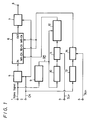
- Fig. 1 shows an overall arrangement of the embodiment of the present invention
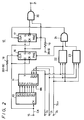
- Figs. 2 and 4 show specific examples of one portion of the embodiment, respectively
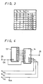
- Fig. 3 is a truth table used to explain the arrangement of Fig. 2.
- a video signal applied to an input terminal 1 is supplied to an analog-to-digital (A/D) converting circuit 5, in which it is converted into a digital video signal by a clock signal (i.e., sampling clock signal) CK supplied thereto from an input terminal 2.
- the frequency of the clock signal CK is, for example, 13.5 MHz.
- the digital video signal from the A/D converting circuit 5 is written in a line memory 6.
- the line memory 6 might be a first-in and first-out (FIFO) type line memory and can store a video signal of 1H where H represents one horizontal cycle period.
- the line memory 6 incorporates therein a read address counter and a write address counter, though not shown.
- a digital-to-analog (D/A) converter 7 is connected to the line memory 6 and converts a read-out output of the line memory 6 into an analog video signal, and this analog video signal is fed to an output terminal 8.
- the aforenoted clock signal CK is also supplied to the D/A converting circuit 7.
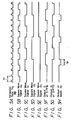
- the video signal applied to the input terminal 1 is supplied to a synchronizing (i.e., sync.) separating circuit 9, and a horizontal synchronizing signal HD ⁇ (see Fig. 5A) separated from the video signal by the circuit 9 is supplied to a counter 10 as a clock signal and is thereby counted.
- a synchronizing i.e., sync.
- the counter 10 is formed of, for example, an 8-bit counter and generates square wave signals Q 0 , Q 1 , Q 2 , ..., Q 7 which result from dividing the horizontal synchronizing signal HD ⁇ from an input terminal 15 by 2, 4, 8, 16, 32, 64 and 128.
- square wave signals Q 0 , Q 1 , Q 2 , ..., Q 7 only the waveforms of the square wave signals Q 0 , Q 1 , Q 2 and Q 3 are illustrated in Figs. 5B, 5C, 5D and 5E, respectively.
- Fig. 3 shows a truth table of logic values of these vertical selecting signals S 0 , S 1 and S 2 of 3 bits and corresponding contents of output signals Y selected from the input signals I 0 , I 1 , I 2 , ...
- the output signal from the data selector 11 is supplied to a pulse width changing circuit 12 and the pulse width thereof is changed to 1H.
- the pulse width changing circuit 12 is supplied with the horizontal synchronizing signal HD ⁇ from the synchronizing separating circuit 9.
- the pulse width changing circuit 11 is comprised of D flip-flop circuits 16, 17, decoders 22, 23, an AND gate 24 and a NAND gate 20.
- the horizontal synchronizing signal HD ⁇ from the input terminal 15 is supplied to clock input terminals of the D flip-flop circuits 16 and 17.
- the output signal Y from the data selector 11 is supplied to a D-input terminal of the D flip-flop circuit 16.
- a clear signal input terminal CLR of the D flip-flop circuit 16 is connected through a resistor 15 to a terminal 30 to which a positive voltage + B (5 Volts) is applied.
- An output Q of the D flip-flop circuit 16 is supplied to a D-input terminal of the D flip-flop circuit 17 of the next stage.
- a preset input terminal PRE of the D flip-flop circuit 17 is connected through a resistor 19 to a terminal 31 to which a positive voltage + B is applied.
- An output Q of the D flip-flop circuit 16 and an output Q ⁇ of the D flip-flop circuit 17 are supplied to the NAND gate 20, and an output terminal 21 is led out from the output side of the NAND gate 20.
- An output developed at the output terminal 21 is supplied to the line memory 6 as a write enable signal (WR-EN).
- the selecting signals S 0 , S 1 and S 2 applied to the input terminal 3 are supplied to decoders 22 and 23.
- a decoded output from the decoder 22 is supplied to the preset input terminal PRE of the D flip-flop circuit 16 and to the AND gate 24, whereas a decoded output from the decoder 23 is supplied to the AND gate 24 whose output is supplied to the clear input terminal CLR of the D flip-flop circuit 17.
- the clock signal CK applied to the input terminal 2 is supplied to and counted by a counter 13.
- the counter 13 is a counter of, for example, 8 bits and generates square wave signals Q 0 , Q 1 , Q 2 , ..., Q 7 which result from dividing the clock signal CK applied to an input terminal 25 by 2, 4, 8, 16, 32, 64, 128 and 256.
- the clock signal CK applied to the input terminal 2 is supplied to and counted by a counter 13.
- the counter 13 is a counter of, for example, 8 bits and generates square wave signals Q 0 , Q 1 , Q 2 , ..., Q 7 which result from dividing the clock signal CK applied to an input terminal 25 by 2, 4, 8, 16, 32, 64, 128 and 256.
- seven square wave signals except the square wave signal Q 7 are supplied to a data selector 14 as input signals I 1 , I 2 , ..., I 7 .
- the input signal I 0 of the data selector 14 becomes the clock signal CK from the input terminal
- the data selector 14 is supplied with horizontal selecting signals SLh (S 0 , S 1 , S 2 ) of 3 bits from an input terminal 4 (i.e., input terminals 4 0 , 4 1 and 4 2 ).
- the output signal Y from the data selector 14 is supplied through an output terminal 26 to the read address counter and to the write address counter incorporated within the line memory 6 of Fig. 1 as read (RD-CK) and write (WR-CK) clock signals.
- the D flip-flop circuit 16 latches the square wave signal Q 1 in response to the leading edge of the horizontal synchronizing signal HD ⁇ (see Fig. 5A) and generates the output Q in which the square wave signal Q 1 is delayed by 90 degrees as shown in Fig. 5F.
- the output Q from the D flip-flop circuit 16 is supplied to the D-input terminal of the D flip-flop circuit 17 and is thereby latched in response to the leading edge of the horizontal synchronizing signal HD ⁇ .
- the D flip-flop circuit 17 generates the output Q ⁇ in which the square wave signal Q of Fig. 5F is delayed by 90 degrees and is inverted in phase as shown in Fig. 5G.
- the output Q of the D flip-flop circuit 16 and the output Q ⁇ of the D flip-flop circuit 17 are supplied to the NAND gate 20, from which there is derived a square wave signal which is opposite in phase to the square wave signal Q 1 and whose pulse width is 1H as shown in Fig. 5H.
- This square wave signal is supplied to the write enable terminal WR-EN of the line memory 6 so that the line memory 6 is set in the write enable mode during a period corresponding to once every 4H periods, thus the incoming digital video signal thus being mosaicked in its vertical direction.
- the output signal Y is presented as the input signals I 2 to I 7 , that is, the outputs Q 1 to Q 6 of the counter 10, the outputs of the decoders 22 and 23 both go “1", accordingly, the output of the AND gate 24 goes “1" so that the D flip-flop circuit 16 is supplied at its preset input terminal PRE with the signal "1” and the D flip-flop circuit 17 is supplied at its clear input terminal CLR with the signal "1".
- the D flip-flop circuits 16 and 17 are inhibited from being preset and cleared, respectively.
- the clock signal CK or one of the outputs Q 0 , Q 1 to Q 6 of the counter 13 is supplied from the data selector 14 to the read and write address counters of the line memory 6 as the write and read clock signals. Consequently, when the line memory 6 is in the writable mode and is supplied with the outputs Q 0 to Q 6 of the counter 13 as the write and read clock signals, one digital pixel signal of the incoming digital video signal is written in the line memory 6 in response to 2, 4, 8, 16, 32, 64 and 128 clock pulses CK, whereby the incoming digital video signal is mosaicked in its horizontal direction.
- the digital pixel signal of the incoming digital video signal is written in the line memory 6 and in response to each arrival of 2, 4, 8, 16, 32, 64 and 128 clock pulses CK, the next digital pixel signal is read out from the line memory 6. Then, the digital pixel signal is held therein during 2, 4, 8, 16, 32, 64 and 128 clock pulses CK are supplied thereto.
- FIFO memory is utilized as the line memory which stores therein the digital video signal of 1H period in the above-mentioned embodiment
- a pair of line memories which store the digital video signal of 1H period and which can not perform the write and read simultaneously may be provided.
- one line memory is used as a write memory and the other line memory is used as a read memory, and during the next 1H period, the said one line memory is used as the read memory and the other line memory is used as the write memory, which is alternately repeated thereafter.
- the vertical selecting signals and the horizontal selecting signals may be determined so that a mosaic effect is achieved only in a desirable region within one frame period.
- a mosaic effect generating apparatus is obtained, in which the arrangement thereof can be simplified, the manufacturing cost thereof can be reduced and the power consumption thereof can be reduced.
Landscapes
- Engineering & Computer Science (AREA)
- Multimedia (AREA)
- Signal Processing (AREA)
- Studio Circuits (AREA)
Claims (9)
- Mosaikeffekt-Erzeugungsvorrichtung, gekennzeichnet durcheinen Zeilenspeicher (6), dem ein ankommendes Videosignal zugeführt wird;eine Taktsignal-Erzeugungseinrichtung (13, 14) zum Erzeugen eines Taktsignales einer vorbestimmten Frequenz und zum Zuführen des Taktsignales zu dem Zeilenspeicher (6) als Schreib-Taktsignal (WR-CK) und Lese-Taktsignal (RD-CK); undeine Schreib-Steuereinrichtung (9-12), die ermöglicht, daß das ankommende Videosignal nur während einer Horizontalzyklusperiode bei jeder Periode einer Vielfachen eines Horizontalzyklus des ankommenden Videosignales in den Zeilenspeicher (6) eingeschrieben wird;dadurch gekennzeichnet, daß die vorbestimmte Frequenz das 1/N-fache einer Abtastfrequenz des ankommenden digitalen Videosignales ist, wobei N eine ganze Zahl größer als 1 ist.
- Mosaikeffekt-Erzeugungsvorrichtung gemäß Anspruch 1,
wobei die Schreib-Steuereinrichtung (9-12) dem Zeilenspeicher (6) ein Steuersignal (WR-EN) zuführen kann, das ermöglicht, daß das ankommende Videosignal nur während einer Horizontalzyklusperiode bei jeder Periode einer Vielfachen eines Horizontalzyklus des ankommenden Videosignales in den Zeilenspeicher (6) eingeschrieben wird. - Mosaikeffekt-Erzeugungsvorrichtung gemäß Anspruch 1 oder 2,
wobei der Zeilenspeicher (6) ein first-in und first-out (FIFO)-Speicher ist. - Mosaikeffekt-Erzeugungsvorrichtung gemäß einem der Ansprüche 1 bis 3,
wobei die Schreib-Steuereinrichtung (9-12) umfaßt:einen Zähler (10), dem ein von dem ankommenden Videosignal abgetrenntes Horizontal-Synchronisiersignal (HD) zugeführt wird und der mehrere Rechteckwellen durch Frequenzteilung des Horizontal-Synchronisiersignales durch mehrere Frequenzteilungsverhältnisse erzeugt;eine Auswahlvorrichtung (11), der ein Ausgangssignal des Zählers (10) zugeführt wird und die eine der mehreren Rechteckwellen auf der Basis eines Vertikal-Auswahlsignales (SLv) erzeugt, das eine Breite des Mosaiks in seiner vertikalen Richtung bestimmt; undeine Pulsbreiten-Änderungsschaltung (12), der ein Ausgangssignal von der Auswahlvorrichtung (11) zugeführt wird und die ein Steuersignal (WR-EN) bildet, das ein Einschreiben in den Zeilenspeicher (6) ermöglicht. - Mosaikeffekt-Erzeugungsvorrichtung gemäß einem der Ansprüche 1 bis 4,
wobei die Taktsignal-Erzeugungseinrichtung (13, 14) umfaßt:
einen Zähler (13), dem ein Referenztaktsignal (CK) zugeführt wird und der mehrere Rechteckwellen durch Frequenzteilen des Referenztaktsignales (CK) durch mehrere Frequenzteilungsverhältnisse erzeugt. - Mosaikeffekt-Erzeugungsvorrichtung gemäß einem der Ansprüche 1 bis 5,
weiterhin aufweisend:einen Analog/Digital-Umsetzer (5), dem ein ankommendes Videosignal zugeführt wird und der das ankommende Videosignal in ein digitales Videosignal umsetzt; undeinen Digital/Analog-Umsetzer (7), dem ein Ausgangssignal des Zeilenspeichers (6) zugeführt wird und der ein aus diesem ausgelesenes digitales Videosignal in ein analoges Videosignal umsetzt. - Mosaikeffekt-Erzeugungsvorrichtung gemäß Anspruch 1,
wobei die Taktsignal-Erzeugungseinrichtung umfaßt:einen ersten Zähler (13), dem ein Referenztaktsignal (CK) zugeführt wird und der mehrere Rechteckwellen durch Frequenzteilen des Referenztaktsignales durch mehrere Frequenzteilungsverhältnisse erzeugt; undeine erste Auswahlvorrichtung (14), der ein Ausgangssignal des ersten Zählers (13) zugeführt wird und die eine der mehreren Rechteckwellen auf der Basis eines Horizontal-Auswahlsignales erzeugt, das eine Breite des Mosaiks in seiner horizontalen Richtung festlegt, und die diese dem Zeilenspeicher (6) als Schreib-Taktsignal (WR-CK) und als Lese-Taktsignal (RD-CK) zuführt;wobei die Schreib-Steuereinrichtung einen zweiten Zähler (10) umfaßt, dem ein von dem ankommenden Videosignal abgetrenntes Horizontal-Synchronisiersiganl (HD) zugeführt wird und der mehrere Rechteckwellen durch Frequenzteilen der Horizontalteilungsverhältnisse erzeugt;eine zweite Auswahlvorrichtung (11), der ein Ausgangssignal des zweiten Zählers zugeführt wird und die eine der mehreren Rechteckwellen auf der Basis eines Vertikal-Auswahlsignales erzeugt, das eine Breite des Mosaiks in seiner vertikalen Richtung festlegt; undeine Pulsbreiten-Änderungsschaltung (12), der ein Ausgangssignal des zweiten Zählers zugeführt wird und die ein Steuersignal bildet, das ein Einschreiben in den Zeilenspeicher (6) ermöglicht, und die dieses dem Zeilenspeicher (6) zuführt. - Mosaikeffekt-Erzeugungsvorrichtung gemäß Anspruch 7,
wobei dem Analog/Digital-Umsetzer (5) und dem Digital/Analog-Umsetzer (7) jeweils das Referenztaktsignal (CK) zugeführt wird. - Mosaikeffekt-Erzeugungsvorrichtung gemäß einem der Ansprüche 1 bis 8,
weiterhin aufweisend eine Einrichtung zum Festlegen der Vertikal-Auswahlsignale und der Horizontal-Auswahlsignale dergestalt, daß ein Mosaikeffekt innerhalb einer Bildperiode nur in einem gewünschten Bereich erreicht wird.
Applications Claiming Priority (2)
| Application Number | Priority Date | Filing Date | Title |
|---|---|---|---|
| JP1262760A JPH03124174A (ja) | 1989-10-07 | 1989-10-07 | モザイク効果装置 |
| JP262760/89 | 1989-10-07 |
Publications (3)
| Publication Number | Publication Date |
|---|---|
| EP0423007A2 EP0423007A2 (de) | 1991-04-17 |
| EP0423007A3 EP0423007A3 (en) | 1992-09-30 |
| EP0423007B1 true EP0423007B1 (de) | 1997-04-16 |
Family
ID=17380209
Family Applications (1)
| Application Number | Title | Priority Date | Filing Date |
|---|---|---|---|
| EP90402780A Expired - Lifetime EP0423007B1 (de) | 1989-10-07 | 1990-10-05 | Anordnung zur Erzeugung von Mosaikeffekten |
Country Status (5)
| Country | Link |
|---|---|
| US (1) | US5148277A (de) |
| EP (1) | EP0423007B1 (de) |
| JP (1) | JPH03124174A (de) |
| KR (1) | KR100232028B1 (de) |
| DE (1) | DE69030478T2 (de) |
Families Citing this family (3)
| Publication number | Priority date | Publication date | Assignee | Title |
|---|---|---|---|---|
| US6535794B1 (en) | 1993-02-23 | 2003-03-18 | Faro Technologoies Inc. | Method of generating an error map for calibration of a robot or multi-axis machining center |
| US5668604A (en) * | 1996-03-27 | 1997-09-16 | Nec Corporation | Horizontal magnifying circuit for video signals |
| KR100459687B1 (ko) * | 1997-07-09 | 2005-01-17 | 삼성전자주식회사 | 모자이크 및 미러 처리기능을 갖는 줌 처리장치 및방법 |
Family Cites Families (7)
| Publication number | Priority date | Publication date | Assignee | Title |
|---|---|---|---|---|
| US4134128A (en) * | 1976-03-19 | 1979-01-09 | Rca Corporation | Television picture size altering apparatus |
| JPS5646367A (en) * | 1979-09-21 | 1981-04-27 | Toshiba Corp | Picture processor |
| JPS5644957A (en) * | 1979-09-21 | 1981-04-24 | Toshiba Corp | Picture processing unit |
| US4782388A (en) * | 1986-10-24 | 1988-11-01 | The Grass Valley Group, Inc. | Method and apparatus for providing video mosaic effects |
| JP2771809B2 (ja) * | 1987-04-17 | 1998-07-02 | ソニー株式会社 | 特殊効果装置 |
| JPH0683470B2 (ja) * | 1987-10-27 | 1994-10-19 | ヤマハ株式会社 | モザイク画像生成回路 |
| JP2710123B2 (ja) * | 1988-01-29 | 1998-02-10 | キヤノン株式会社 | 画像拡大装置 |
-
1989
- 1989-10-07 JP JP1262760A patent/JPH03124174A/ja active Pending
-
1990
- 1990-09-27 KR KR1019900015342A patent/KR100232028B1/ko not_active Expired - Fee Related
- 1990-10-03 US US07/592,254 patent/US5148277A/en not_active Expired - Fee Related
- 1990-10-05 DE DE69030478T patent/DE69030478T2/de not_active Expired - Fee Related
- 1990-10-05 EP EP90402780A patent/EP0423007B1/de not_active Expired - Lifetime
Also Published As
| Publication number | Publication date |
|---|---|
| KR910009064A (ko) | 1991-05-31 |
| EP0423007A2 (de) | 1991-04-17 |
| DE69030478T2 (de) | 1997-10-02 |
| KR100232028B1 (ko) | 1999-12-01 |
| JPH03124174A (ja) | 1991-05-27 |
| EP0423007A3 (en) | 1992-09-30 |
| US5148277A (en) | 1992-09-15 |
| DE69030478D1 (de) | 1997-05-22 |
Similar Documents
| Publication | Publication Date | Title |
|---|---|---|
| US4745485A (en) | Picture display device | |
| EP0291252A2 (de) | Verfahren und Gerät zur Fernsehwiedergabe | |
| EP0345807B1 (de) | Zeilenspeicher für Geschwindigkeitsumwandlung | |
| US4369504A (en) | Serial-parallel signal converter | |
| JP3016694B2 (ja) | ダブルスキャン回路 | |
| US5153574A (en) | Interface for a thin display | |
| US4677493A (en) | Picture information processing system | |
| US4618859A (en) | Graphic display unit | |
| US5148277A (en) | Mosaic effect generating apparatus | |
| US5055940A (en) | Video memory control apparatus | |
| US4908614A (en) | Image data output apparatus | |
| EP0420281B1 (de) | Wellenformanzeigeschaltung mit Luminanzinterpolation | |
| JPH0761141B2 (ja) | ビデオメモリ | |
| US5216506A (en) | Programmable device for storing digital video lines | |
| JPH0535214A (ja) | 液晶表示装置 | |
| JPH1063219A (ja) | 表示装置及びその駆動方法 | |
| JP3241065B2 (ja) | ラインメモリ | |
| JPS6020680A (ja) | 画像処理装置 | |
| JPS61237539A (ja) | フレ−ム変換回路 | |
| GB2269507A (en) | Coding a video signal to facilitate aspect ratio conversion | |
| JP3311555B2 (ja) | イメージメモリ読み出し回路 | |
| JPS61166278A (ja) | 2画面テレビ受信機 | |
| JPH06233153A (ja) | 同期信号発生回路 | |
| JPS59214087A (ja) | 色彩画像の記憶方式 | |
| JPH08328538A (ja) | 画像表示装置 |
Legal Events
| Date | Code | Title | Description |
|---|---|---|---|
| PUAI | Public reference made under article 153(3) epc to a published international application that has entered the european phase |
Free format text: ORIGINAL CODE: 0009012 |
|
| AK | Designated contracting states |
Kind code of ref document: A2 Designated state(s): DE FR GB |
|
| PUAL | Search report despatched |
Free format text: ORIGINAL CODE: 0009013 |
|
| AK | Designated contracting states |
Kind code of ref document: A3 Designated state(s): DE FR GB |
|
| 17P | Request for examination filed |
Effective date: 19930304 |
|
| 17Q | First examination report despatched |
Effective date: 19950214 |
|
| GRAG | Despatch of communication of intention to grant |
Free format text: ORIGINAL CODE: EPIDOS AGRA |
|
| GRAH | Despatch of communication of intention to grant a patent |
Free format text: ORIGINAL CODE: EPIDOS IGRA |
|
| GRAH | Despatch of communication of intention to grant a patent |
Free format text: ORIGINAL CODE: EPIDOS IGRA |
|
| GRAA | (expected) grant |
Free format text: ORIGINAL CODE: 0009210 |
|
| AK | Designated contracting states |
Kind code of ref document: B1 Designated state(s): DE FR GB |
|
| REF | Corresponds to: |
Ref document number: 69030478 Country of ref document: DE Date of ref document: 19970522 |
|
| ET | Fr: translation filed | ||
| PLBE | No opposition filed within time limit |
Free format text: ORIGINAL CODE: 0009261 |
|
| STAA | Information on the status of an ep patent application or granted ep patent |
Free format text: STATUS: NO OPPOSITION FILED WITHIN TIME LIMIT |
|
| 26N | No opposition filed | ||
| PGFP | Annual fee paid to national office [announced via postgrant information from national office to epo] |
Ref country code: GB Payment date: 20011003 Year of fee payment: 12 |
|
| PGFP | Annual fee paid to national office [announced via postgrant information from national office to epo] |
Ref country code: FR Payment date: 20011010 Year of fee payment: 12 |
|
| PGFP | Annual fee paid to national office [announced via postgrant information from national office to epo] |
Ref country code: DE Payment date: 20011022 Year of fee payment: 12 |
|
| REG | Reference to a national code |
Ref country code: GB Ref legal event code: IF02 |
|
| PG25 | Lapsed in a contracting state [announced via postgrant information from national office to epo] |
Ref country code: GB Free format text: LAPSE BECAUSE OF NON-PAYMENT OF DUE FEES Effective date: 20021005 |
|
| PG25 | Lapsed in a contracting state [announced via postgrant information from national office to epo] |
Ref country code: DE Free format text: LAPSE BECAUSE OF NON-PAYMENT OF DUE FEES Effective date: 20030501 |
|
| GBPC | Gb: european patent ceased through non-payment of renewal fee |
Effective date: 20021005 |
|
| PG25 | Lapsed in a contracting state [announced via postgrant information from national office to epo] |
Ref country code: FR Free format text: LAPSE BECAUSE OF NON-PAYMENT OF DUE FEES Effective date: 20030630 |
|
| REG | Reference to a national code |
Ref country code: FR Ref legal event code: ST |