EP0423730A2 - Dispositif électronique à fonction de transmission de données - Google Patents
Dispositif électronique à fonction de transmission de données Download PDFInfo
- Publication number
- EP0423730A2 EP0423730A2 EP90119845A EP90119845A EP0423730A2 EP 0423730 A2 EP0423730 A2 EP 0423730A2 EP 90119845 A EP90119845 A EP 90119845A EP 90119845 A EP90119845 A EP 90119845A EP 0423730 A2 EP0423730 A2 EP 0423730A2
- Authority
- EP
- European Patent Office
- Prior art keywords
- data
- frame
- communications
- electronic device
- data transmission
- Prior art date
- Legal status (The legal status is an assumption and is not a legal conclusion. Google has not performed a legal analysis and makes no representation as to the accuracy of the status listed.)
- Granted
Links
Images


Classifications
-
- H—ELECTRICITY
- H04—ELECTRIC COMMUNICATION TECHNIQUE
- H04L—TRANSMISSION OF DIGITAL INFORMATION, e.g. TELEGRAPHIC COMMUNICATION
- H04L12/00—Data switching networks
- H04L12/28—Data switching networks characterised by path configuration, e.g. LAN [Local Area Networks] or WAN [Wide Area Networks]
- H04L12/40—Bus networks
- H04L12/403—Bus networks with centralised control, e.g. polling
Definitions
- the present invention relates to an electronic device with a communications function to transmit data by a transmitting means to an audio visual device in a domestic data communications network system.
- a domestic Digital Bus (IEC 84 (Secretariat) 86I,II; Draft-Domestic Digital Bus (D2B)) has been known to communicate data between audio visual devices (referred to as AV devices hereinafter) connected to a common signal transmission path.
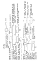
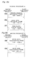
- the AV device provided with such communications means as above has generally worked in the systematic structure illustrated in Fig. 10 through connection via a bus line.
- a frame which is formed in the structure shown in Fig. 11 is used and the data are stored in a data field (DF) 123 of the frame from a master transmitter side to a slave receiver side.
- DF data field
- the structure of the frame shown in Fig. 11 is common to the embodiment of the present invention.
- the master (electronic device (1)) 101 reads out a part of the content stored in a memory unit of the slave (electronic device (2)) 102.
- the master transmits a memory address designating frame 135 shown in Figs. 13a and 13b, then a read data requiring frame 136 and a read slave status frame 137 to the slave 136.
- a preliminarily defined 12-bit address of the master (electronic device (1)) 101 is stored in a master address 115 in Fig.
- a preliminarily-defined 12-bit address of the slave (electronic device (2)) 102 into a slave address 116, a code (b3b2b1b0 '1000'B) indicating a write memory address with lock (WMA+L) shown in Fig. 12 into a control bit 117, and a memory read address preliminarily defined 1:1 corresponding to the content of the memory unit which the master (electronic device (1)) 101 desires to read out from the slave (electronic device (2)) 102 into a data bit 118, respectively.
- the data bit 118 of the memory address designating frame 135 is transferred in a direction of the write action (MS)131 of Fig. 11, while the data bit 118 of the read data requiring frame 136 is transferred in a direction of the read action (SM)132 shown in Fig. 11.
- the data bit 118 of the read slave status frame 137 is transferred in the (SM)132 direction.
- the read slave status frame 137 is used so as to release an indication of the master that the slave be locked.
- the master (electronic device (1)) 101 simply transfers the data to the slave (electronic device (2)) 102 through consecutive transmission of one or a plurality of write data transferring frames 138 and one write data transferring frame 139 of Fig. 13b.
- a preliminarily defined 12-bit address of the master (electronic device (1)) 101 is stored in the master address 115 of each of the write data transferring frames 138 and write data transferring frame 139
- a preliminarily defined 12-bit address of the slave (electronic device (2)) 102 is stored in the slave address 116 of each frame.
- the present invention has been developed with a view to substantially eliminating the above-described disadvantages inherent in the prior art, and has for its essential object to provide an electronic device with a uniform data transmission function adapted to communicate data through memory access, while solving complexities in actual installation and communications process, wherein a communications means is constituted in a manner to realize transmission of both data and command in the communications process.
- a format is defined so that a data field (DF) of a memory access designating frame sent from a master to a slave is provided with a writing unit of data related to the type of access, i.e., reading or writing and a memory storing address. It is so arranged in the electronic device of the present invention that the memory access designating frames are preliminarily transferred commonly before the transmission of a read data requiring frame or a write data transferring frame.
- a device unit of the electronic device of the present invention which unit provides a communications means for executing data transmission is constituted at least of a device controlling part, a data transmission processing part and a communications part.
- the master indicates either writing or reading of data to the slave when the data are to be transmitted between the master electronic device and the slave electronic device
- the type of access and a memory storing address at the slave side are sent from the device controlling part of the master to the data transmission processing part, thereby starting the memory access communications process for the data transmission.
- the data to be transferred are also sent from the device controlling part to the data transmission processing part. Consequently, the data transmission processing part assembles a memory access designating frame based on the transmission informations sent from the master side and sends the same to a data transmission processing part of the slave through a communications part.
- the data transmission processing part at the slave side discriminates the type of access in preparation for every process to receive a write data transferring frame or a read data requiring frame subsequently sent from the master. After the data are completely transferred between the master and slave sides by the write data transferring frame or read data requiring frame, each data transmission processing part of the master and slave sides informs the result of communications, i.e., the content of the data, to the respective device controlling part. In this manner, writing or reading of the data is realized.
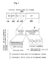
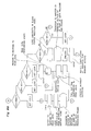
- Fig. 1 there is shown a logical structure of a memory access designating (R) frame/memory access designating (W) frame according to one preferred embodiment of the present invention.
- a format of a data field is shown as well.
- the detailed format and definition of each field constituting the above frame are the same as in the conventional example shown in Figs. 11 and 12 except the definition of DF123 when a control bit 117 represents (WMA+L).
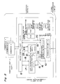
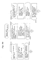
- Fig. 2 illustrates the structure of a device unit which offers a communications means in an electronic device of the present embodiment.
- Figs. 3a and 3b explain the communications sequence in each of reading and writing operations during data transmission between a master electronic device and a slave electronic device.
- Figs. 4a, 4b and 4c taken together shows the transition of the receiving state of the frame in a data transmission processing part of the device unit of Fig. 2 based on SDL description (CCITT, Z series recommendation).
- Figs. 5a and 5b taken together is a diagram showing the transition of the transmitting state of the frame in the data transmission processing part of Fig. 2 on SDL description.
- Figs. 6a, 6b and 6c taken together is a SDL description showing the transition of the receiving state in a communications controlling part within a communications unit in Fig. 2
- Fig. 7 is a SDL description showing the transition of the transmitting state in the communications controlling part within the communications unit of Fig. 2
- Fig. 8 is a SDL description showing the transition of the receiving state in the device controlling part of Fig. 2
- Fig. 9 is a SDL description showing the transition of the transmitting state in the device controlling part of Fig. 2.
- numeral 1 represents a part of the components constituting a data field (DF) 123 in a memory access designating (R) frame/memory access designating (W) frame, and particularly representing the type of access (ATP) to identify whether a frame transferred from the master to the slave subsequent to the memory access designating frame is a read data requiring frame which requires the data to be read out from the slave or a write data transferring frame which requires the data to be written into the slave.
- the type of access 1 designates reading of data
- a read address in a memory area of the slave side which the master reads is stored in a memory storing address (MSA) 2 as an access address.
- MSA memory storing address
- an electronic device 3 is consisted of a device unit 4 and a subdevice unit 11.
- the device units 4 with a data transmission function are connected each other via a common signal transmission path 27.
- the subdevice unit 11 carries out control of the whole device.
- the device unit 4 functions as a communications means, having a communications unit 5, a data transmission processing part 6 and a device controlling part 8.
- the device unit 4 further includes a memory area 7 for use as a storing area of the data transmitted between the master and slave, a frame receiving buffer 12, a frame transmitting buffer 13, a read responding buffer 14, a read data storing buffer 25 and a slave status register 26.
- the device unit 4 works as an interface with the subdevice unit 11.
- the communications unit 5 is provided with a transceiver unit 9 and a communications controlling part 10.
- the data transmission processing part 6 which is a main component of the electronic device of the present embodiment is positioned between the communications controlling part 10 and device controlling part 8, with managing and processing each communications sequence in reading and writing the data between the master and slave through memory access.
- Informations necessary for the communications process are sent and received between the data transmission processing part 6 and communications controlling part 10 via signals 15 and 16 and various kinds of registers 12, 13, 14, 25 and 26.
- informations necessary for transmission of data are sent and received between the data transmission processing part 6 and device controlling part 8 via signals 17 and 18 and memory area 7 where the data to be read or written are transferred between the master and slave.
- the memory area (MEM) 7 stores data to be written by the master into the slave.
- the data are given from the device controlling part 8 at the master side via a signal 24 and sent to the data transmission processing part 6 via a signal 22.
- the memory area (MEM) 7 stores data to be read out by the master from the slave.
- the data read from the slave side extracted from a receiving frame of the data transmission processing part 6 at the master side are stored in MEM 7 via a signal 21 and sent to the device controlling part 8 which indicates reading of the data via a signal 23.
- the master indicates the slave side to read data
- the data to be read are preliminarily stored and retained in MEM 7 before the data transmission processing part 6 at the slave side reads the data via a signal 22.
- the device controlling part (DCP) 8 sends a command generated from a subdevice unit 11 or from itself to a communications controlling part 10 via the frame transmitting buffer 13 and a signal 20 requiring transmission of the command, and at the same time, receives and processes the content of a frame including the command and received by the communications controlling part 10 via the frame receiving buffer 12 and a signal 19 notifying the receipt of the command, while indicating reading of the data from the master to the slave via signals 18, 24 and 22 and memory area 7 when such an indication is generated from the subdevice unit 11 or by itself, or indicating reading of the data via signals 18, 21 and 23 and memory area 7. Furthermore, when the data are written from the master to the slave, DCP 8 is informed of the completion of the writing process at the data transmission processing part 6 to the memory area 7 via a signal 17.
- a transceiver unit 9 is connected to the signal transmission path 27, working as an interface of electrophyscial conditions.
- the communications controlling part (CCP) 10 offers a communications controlling function necessary for transmission of the content of DF 123 of the frame of Fig. 1 between the master and slave in a transparent manner.
- the CCP 10 is connected to the data transmission processing part 6 and device controlling part 8, with making an access to the various kinds of registers, so that CCP 10 functions at least to indicate processing of a receiving frame to the data transmission processing part 6 when the content indicated by a control bit CB 122 of the receiving frame through the signal transmission path 27 is a memory address with lock (WMA+L), a read data with lock (RD+L) or a write data with lock (WD+L), or to indicate processing of the frame directly to the device controlling part 8 when the content indicated by the control bit is a write command with lock (WC+L).
- WMA+L memory address with lock
- R+L read data with lock
- WD+L write data with lock
- the subdevice unit 11 is comprised of various kinds of controlling circuits as subdevices such as a deck controlling circuit, a tuner controlling circuit, audio signal controlling circuit, video signal controlling circuit, input/output manipulation display controlling circuit, etc.
- the controlling circuits are classified for every function common or peculiar to an audio visual device.
- data can be transferred between the master and slave or a command is required to be transmitted or received.
- the frame receiving buffer (RXB) 12 is employed at the communications controlling part 10 and data transmission processing part 6 to temporarily store the content of the frame 124 of Fig. 1 in the event that the frame is to be received.
- the frame transmitting buffer (TXB) 13 is employed at the device controlling part 8 and data transmission processing part 6 to temporarily store the content of the frame 124 of Fig. 1 in the event that the frame is to be transmitted.
- the read responding buffer 14 is used to temporarily store the data to be transferred to the slave at a read action section in DF 123 of a read data requiring frame.
- the read data storing buffer 25 is used, in contrast to the buffer 14, to temporarily store the data of DF 123 of the read data requiring frame transferred from the slave side when the read data requiring frame is transmitted by the master.
- the slave status register 26 sequentially holds and memorizes the state of the frame receiving buffer (RXB) 12 as to whether it is vacant, or the state of the communications controlling part 10 as to whether it is locked or unlocked, with maintaining informations of a predetermined format.
- a plurality of electronic devices 3 are connected each other via the respective communications units 5 through the common signal transmission line 27, so that data are transmitted between the master and slave devices.
- the signal transmission line 27 is identical to the signal transmission line 100 shown in Fig. 10.
- a signal 16 transmits at least five kinds of requirements (requirement of transmission of a memory access designating (W) frame, requirement of transmission of a memory access designating (R) frame, requirement of transmission of a write data transferring frame, requirement of transmission of a read data requiring frame, and requirement of transmission of a lock release RSS frame) when the frame is transmitted from the data transmission processing part (DPT) 6 to the communications controlling part (CCP) 10.
- the signal 16 also transmits a notification of responding to the read data when the frame is received.
- the signal 17 transmits at least two kinds of notifications (notification of completion of transmission of a write data and notification of completion of transmission of a read data requiring frame) when the frame is transmitted from the data transmission processing part (DCP) 6 to the device controlling part (DCP) 8, and at least two kinds of notifications (notification of completion of receipt of a write data and notification of completion of receipt of a read data) when the frame is received.
- the signal 18 is used to transmit at least three kinds of requirements/indications (requirement of indication of a write data, requirement of indication of a read data and indication of completion of requirement of a read data) only when the frame is transmitted from the device controlling part (DCP) 8 to the data transmission processing part (DTP) 6.
- a notification of completion of a read data of at least one frame is issued by the signal 19 when the frame is transmitted from the communications controlling part (CCP) 10 to the device controlling part (DCP) 8. Furthermore, when the frame is received, the signal 19 issues at least a notification of completion of receipt of the command.
- the signal 20 is used so that at least two kinds of requirements (requirement of transmission of a command frame and requirement of transmission of a lock release RSS frame) are issued only when the frame is transmitted from DCP 8 to CCP 10.
- the signal 21 sends informations of a memory storing address and a write data to be written at the slave side which is transferred from the master side, thus allowing the data transmission processing part (DTP) 6 to read/write data to the memory area (MEM) 7.
- DTP data transmission processing part
- MEM memory area
- the signal 22 sends from the memory area (MEM) 7 to the data transmission processing part (DTP) 6 at least a read data to be read which is necessary in preparation for DTP 6 at the slave side to respond at least to the requirement of the read data from the master side.
- MEM memory area
- DTP data transmission processing part
- DCP 8 When the device controlling part (DCP) 8 receives the notification of completion of receiving process of a read data from DTP 6, at least the read data is fed from the memory area (MEM) 7 to DCP 8 by the signal 23.
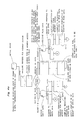
- the memory access designating (R) frame 28 is used first when the master starts to read the content of a specific data preliminarily defined in the memory area (MEM) 7 of Fig. 2 in the slave electronic device.
- the memory storing address (MSA) 2 at the slave side into which the data are read is set succeeding to the ATP 1 in the frame 28.
- the frame 29 is a read data requiring frame in which the control bit 117 of Fig. 11 is (RD+L) of Fig. 12, and which is used when the master reads the data from the slave side using the read action section (SM) 132 of the data field DF 123 in Fig. 11.
- SM read action section
- the lock release RSS frame 30 is used to notify the completion of a series of reading procedures from the master to the slave by the memory access designating (R) frame 28 and read data requiring frame 29 and to indicate release of the locking state of the slave by the master side.
- the frame 31 is first used to transmit the data from the master to the slave when the data are written into a specific storing area preliminarily defined in the memory area (MEM) 7 shown in Fig. 2.
- the memory storing address (MSA) 2 at the slave side into which the data are written is set following the ATP 1.
- the frame 32 which is a write data transferring frame used by the master when the data are written into the slave side using a write action section (MS) 131 of the data field DF 123 of Fig. 11.
- the frame 32 has the control bit 117 of Fig. 11 to represent (WD+L) of Fig. 12.
- the lock release RSS frame 33 in the same format as the frame 30 is used to notify the completion of a series of writing procedures by the master to the slave by the memory access designating (W) frame 31 and write data transmitting frame 32, and to indicate release of the lock of the slave by the master.
- CCP 10 carries out the operation for transition thereof into the receiving state as shown in Figs. 6a, 6b and 6c when a frame is to be received between the master and slave via the transceiver unit 9 through the signal transmission line 27.
- CCP 10 carries out the operation for transition therof into the transmitting state as depicted in Fig. 7.
- the data transmission processing part (DTP) 6 is positioned between the device controlling part (DCP) 8 and communications controlling part (CCP) 10, and is responsible for the whole writing/reading processes including management of the procedures therefor.
- DTP 6 when the frame is to be received, DTP 6 carries out the operation of transition thereof into the receiving state in accordance with a flow of Figs. 4a, 4b and 4c, while performing the operation for transition into the transmitting state shown in Figs. 5a and 5b when the frame is to be transmitted.
- DCP 8 performs the operation for transition into the receiving state as the receiving process in reading or writing the data as indicated in Fig. 8 and the operation for transition into the transmitting state as shown in Fig. 9 as the transmitting process.
- the master side and slave side will operate in compliance with respective flows indicated in Figs. 4 through 9.
- DCP 8 notifies the necessary processing result to the subdevice unit (SDP) 11 by the use of a communications procedure or the like.
- SDP subdevice unit
- DCP device controlling part
- DTP data transmission processing part
- CCP communications controlling part
- Each component is constructed independently of exclusive hardware logic.
- Each component is constituted independently as a software/firmware of a microprocessor of 16 bits, 8 bits, 4 bits, etc.
- Two of the DCP 8, DTP 6 and CCP 10 are constructed based on special hardware logic, and the remaining one is formed of a software/firmware of a microprocessor.
- Two of the DCP 8, DTP 6 and CCP 10 are formed of a hardware/firmware of a special or general-purpose microprocessor, and the remaining one is constructed according to hardware logic.
- All of the DCP 8, DTP 6 and CCP 10 are constituted of a software/firmware of a single special or general-use microprocessor, or based on single special hardware logic.
- the present invention provides a communications means which has a function realizing easy transmission of data.
Landscapes
- Engineering & Computer Science (AREA)
- Computer Networks & Wireless Communication (AREA)
- Signal Processing (AREA)
- Communication Control (AREA)
- Selective Calling Equipment (AREA)
- Multi Processors (AREA)
- Computer And Data Communications (AREA)
- Small-Scale Networks (AREA)
Applications Claiming Priority (2)
| Application Number | Priority Date | Filing Date | Title |
|---|---|---|---|
| JP1269344A JPH0732397B2 (ja) | 1989-10-17 | 1989-10-17 | データ伝送機能付き電子機器 |
| JP269344/89 | 1989-10-17 |
Publications (3)
| Publication Number | Publication Date |
|---|---|
| EP0423730A2 true EP0423730A2 (fr) | 1991-04-24 |
| EP0423730A3 EP0423730A3 (en) | 1993-07-14 |
| EP0423730B1 EP0423730B1 (fr) | 1998-03-04 |
Family
ID=17471073
Family Applications (1)
| Application Number | Title | Priority Date | Filing Date |
|---|---|---|---|
| EP90119845A Expired - Lifetime EP0423730B1 (fr) | 1989-10-17 | 1990-10-16 | Dispositif électronique à fonction de transmission de données |
Country Status (4)
| Country | Link |
|---|---|
| EP (1) | EP0423730B1 (fr) |
| JP (1) | JPH0732397B2 (fr) |
| CA (1) | CA2027740C (fr) |
| DE (1) | DE69032078T2 (fr) |
Cited By (3)
| Publication number | Priority date | Publication date | Assignee | Title |
|---|---|---|---|---|
| EP0651588A3 (fr) * | 1993-10-30 | 1996-06-05 | Sony Corp | Procédé de communication dans un système bus bidirectionnel. |
| WO1997047156A3 (fr) * | 1996-06-07 | 1998-02-19 | Madge Networks Ltd | Systeme de communication comprenant un reseau et un processeur d'appels |
| EP0841791A4 (fr) * | 1996-04-04 | 2000-08-16 | Sony Corp | Controleur de communications et procede de controle des communications |
Families Citing this family (1)
| Publication number | Priority date | Publication date | Assignee | Title |
|---|---|---|---|---|
| JP6988124B2 (ja) * | 2017-03-27 | 2022-01-05 | カシオ計算機株式会社 | 通信装置、電子時計、通信方法、及びプログラム |
Family Cites Families (3)
| Publication number | Priority date | Publication date | Assignee | Title |
|---|---|---|---|---|
| JPS6450152A (en) * | 1987-08-20 | 1989-02-27 | Fujitsu Ltd | Communication controller |
| FR2627039B1 (fr) * | 1988-02-10 | 1994-01-21 | Peugeot Automobiles | |
| NL8800639A (nl) * | 1988-03-16 | 1989-10-16 | Philips Nv | Eenkanaalskommunikatiebussysteem en station voor gebruik in zo een kommunikatiebussysteem. |
-
1989
- 1989-10-17 JP JP1269344A patent/JPH0732397B2/ja not_active Expired - Lifetime
-
1990
- 1990-10-16 CA CA002027740A patent/CA2027740C/fr not_active Expired - Lifetime
- 1990-10-16 DE DE69032078T patent/DE69032078T2/de not_active Expired - Lifetime
- 1990-10-16 EP EP90119845A patent/EP0423730B1/fr not_active Expired - Lifetime
Cited By (3)
| Publication number | Priority date | Publication date | Assignee | Title |
|---|---|---|---|---|
| EP0651588A3 (fr) * | 1993-10-30 | 1996-06-05 | Sony Corp | Procédé de communication dans un système bus bidirectionnel. |
| EP0841791A4 (fr) * | 1996-04-04 | 2000-08-16 | Sony Corp | Controleur de communications et procede de controle des communications |
| WO1997047156A3 (fr) * | 1996-06-07 | 1998-02-19 | Madge Networks Ltd | Systeme de communication comprenant un reseau et un processeur d'appels |
Also Published As
| Publication number | Publication date |
|---|---|
| DE69032078T2 (de) | 1998-08-20 |
| CA2027740A1 (fr) | 1991-04-18 |
| DE69032078D1 (de) | 1998-04-09 |
| EP0423730A3 (en) | 1993-07-14 |
| EP0423730B1 (fr) | 1998-03-04 |
| CA2027740C (fr) | 1994-12-27 |
| JPH0732397B2 (ja) | 1995-04-10 |
| JPH03132126A (ja) | 1991-06-05 |
Similar Documents
| Publication | Publication Date | Title |
|---|---|---|
| US5689244A (en) | Communication system and electronic apparatus | |
| US5132905A (en) | System and method applicable to vehicles for communicating between data processing stations | |
| US6157650A (en) | Method and apparatus for connecting network | |
| US5828656A (en) | Method of controlling communications, and electronic device | |
| JPS6194433A (ja) | シリアルバスの制御方式 | |
| US5313408A (en) | Multistation display system for controlling a display monitor associated with plural audio video devices | |
| EP0390567A2 (fr) | Dispositif électronique avec fonction de communication du type à commande exclusive et son système de communication | |
| JPH03206751A (ja) | ループ式データリンクシステムの局番設定方法 | |
| EP0423730A2 (fr) | Dispositif électronique à fonction de transmission de données | |
| US5214644A (en) | Electronic device with data transmission function | |
| EP0336547B1 (fr) | Réseau ordinateur et méthode pour son opération | |
| US5165032A (en) | Process and device for hierarchized access to a network for transmission of information | |
| JP3380957B2 (ja) | 二重化通信制御装置 | |
| JP2000134277A (ja) | 通信リンク自動識別方法及びそのシステム | |
| EP0482951B1 (fr) | Méthode et système pour la communication de données dans un réseau de communication d'une automobile | |
| JPH01177296A (ja) | 遠方監視制御システム | |
| CA2354102C (fr) | Systeme de communication et appareil electronique | |
| JPH0234518B2 (fr) | ||
| JPS59161952A (ja) | 通信パス確立方式 | |
| JP3178206B2 (ja) | 多重通信装置 | |
| JP2590773B2 (ja) | ファクシミリ通信システム | |
| JPH02250450A (ja) | 監視方式 | |
| JPS6142466B2 (fr) | ||
| JPS61108239A (ja) | 通信主局権利の委譲方法 | |
| JPH0253358A (ja) | Mfc信号監視方式 |
Legal Events
| Date | Code | Title | Description |
|---|---|---|---|
| PUAI | Public reference made under article 153(3) epc to a published international application that has entered the european phase |
Free format text: ORIGINAL CODE: 0009012 |
|
| 17P | Request for examination filed |
Effective date: 19901016 |
|
| AK | Designated contracting states |
Kind code of ref document: A2 Designated state(s): DE FR GB NL |
|
| PUAL | Search report despatched |
Free format text: ORIGINAL CODE: 0009013 |
|
| AK | Designated contracting states |
Kind code of ref document: A3 Designated state(s): DE FR GB NL |
|
| 17Q | First examination report despatched |
Effective date: 19941222 |
|
| GRAG | Despatch of communication of intention to grant |
Free format text: ORIGINAL CODE: EPIDOS AGRA |
|
| GRAG | Despatch of communication of intention to grant |
Free format text: ORIGINAL CODE: EPIDOS AGRA |
|
| GRAH | Despatch of communication of intention to grant a patent |
Free format text: ORIGINAL CODE: EPIDOS IGRA |
|
| GRAH | Despatch of communication of intention to grant a patent |
Free format text: ORIGINAL CODE: EPIDOS IGRA |
|
| GRAA | (expected) grant |
Free format text: ORIGINAL CODE: 0009210 |
|
| AK | Designated contracting states |
Kind code of ref document: B1 Designated state(s): DE FR GB NL |
|
| ET | Fr: translation filed | ||
| REF | Corresponds to: |
Ref document number: 69032078 Country of ref document: DE Date of ref document: 19980409 |
|
| PLBE | No opposition filed within time limit |
Free format text: ORIGINAL CODE: 0009261 |
|
| STAA | Information on the status of an ep patent application or granted ep patent |
Free format text: STATUS: NO OPPOSITION FILED WITHIN TIME LIMIT |
|
| 26N | No opposition filed | ||
| REG | Reference to a national code |
Ref country code: GB Ref legal event code: IF02 |
|
| PGFP | Annual fee paid to national office [announced via postgrant information from national office to epo] |
Ref country code: DE Payment date: 20091008 Year of fee payment: 20 |
|
| PGFP | Annual fee paid to national office [announced via postgrant information from national office to epo] |
Ref country code: NL Payment date: 20091015 Year of fee payment: 20 |
|
| PGFP | Annual fee paid to national office [announced via postgrant information from national office to epo] |
Ref country code: GB Payment date: 20091014 Year of fee payment: 20 Ref country code: FR Payment date: 20091029 Year of fee payment: 20 |
|
| REG | Reference to a national code |
Ref country code: NL Ref legal event code: V4 Effective date: 20101016 |
|
| REG | Reference to a national code |
Ref country code: GB Ref legal event code: PE20 Expiry date: 20101015 |
|
| PG25 | Lapsed in a contracting state [announced via postgrant information from national office to epo] |
Ref country code: NL Free format text: LAPSE BECAUSE OF EXPIRATION OF PROTECTION Effective date: 20101016 |
|
| PG25 | Lapsed in a contracting state [announced via postgrant information from national office to epo] |
Ref country code: GB Free format text: LAPSE BECAUSE OF EXPIRATION OF PROTECTION Effective date: 20101015 |
|
| PG25 | Lapsed in a contracting state [announced via postgrant information from national office to epo] |
Ref country code: DE Free format text: LAPSE BECAUSE OF EXPIRATION OF PROTECTION Effective date: 20101016 |