EP0424485B1 - Vollverdiefte verbindungsstruktur mit titanium/wolfram und selektivem cvd-wolfram - Google Patents
Vollverdiefte verbindungsstruktur mit titanium/wolfram und selektivem cvd-wolfram Download PDFInfo
- Publication number
- EP0424485B1 EP0424485B1 EP90905128A EP90905128A EP0424485B1 EP 0424485 B1 EP0424485 B1 EP 0424485B1 EP 90905128 A EP90905128 A EP 90905128A EP 90905128 A EP90905128 A EP 90905128A EP 0424485 B1 EP0424485 B1 EP 0424485B1
- Authority
- EP
- European Patent Office
- Prior art keywords
- layer
- metal
- adhesion layer
- depositing
- adhesion
- Prior art date
- Legal status (The legal status is an assumption and is not a legal conclusion. Google has not performed a legal analysis and makes no representation as to the accuracy of the status listed.)
- Expired - Lifetime
Links
Images

Classifications
-
- H—ELECTRICITY
- H10—SEMICONDUCTOR DEVICES; ELECTRIC SOLID-STATE DEVICES NOT OTHERWISE PROVIDED FOR
- H10W—GENERIC PACKAGES, INTERCONNECTIONS, CONNECTORS OR OTHER CONSTRUCTIONAL DETAILS OF DEVICES COVERED BY CLASS H10
- H10W20/00—Interconnections in chips, wafers or substrates
- H10W20/01—Manufacture or treatment
- H10W20/031—Manufacture or treatment of conductive parts of the interconnections
- H10W20/056—Manufacture or treatment of conductive parts of the interconnections by filling conductive material into holes, grooves or trenches
- H10W20/057—Manufacture or treatment of conductive parts of the interconnections by filling conductive material into holes, grooves or trenches by selectively depositing, e.g. by using selective CVD or plating
-
- H—ELECTRICITY
- H10—SEMICONDUCTOR DEVICES; ELECTRIC SOLID-STATE DEVICES NOT OTHERWISE PROVIDED FOR
- H10P—GENERIC PROCESSES OR APPARATUS FOR THE MANUFACTURE OR TREATMENT OF DEVICES COVERED BY CLASS H10
- H10P14/00—Formation of materials, e.g. in the shape of layers or pillars
- H10P14/40—Formation of materials, e.g. in the shape of layers or pillars of conductive or resistive materials
- H10P14/412—Deposition of metallic or metal-silicide materials
-
- H—ELECTRICITY
- H10—SEMICONDUCTOR DEVICES; ELECTRIC SOLID-STATE DEVICES NOT OTHERWISE PROVIDED FOR
- H10W—GENERIC PACKAGES, INTERCONNECTIONS, CONNECTORS OR OTHER CONSTRUCTIONAL DETAILS OF DEVICES COVERED BY CLASS H10
- H10W20/00—Interconnections in chips, wafers or substrates
- H10W20/01—Manufacture or treatment
- H10W20/031—Manufacture or treatment of conductive parts of the interconnections
- H10W20/032—Manufacture or treatment of conductive parts of the interconnections of conductive barrier, adhesion or liner layers
- H10W20/033—Manufacture or treatment of conductive parts of the interconnections of conductive barrier, adhesion or liner layers in openings in dielectrics
-
- H—ELECTRICITY
- H10—SEMICONDUCTOR DEVICES; ELECTRIC SOLID-STATE DEVICES NOT OTHERWISE PROVIDED FOR
- H10W—GENERIC PACKAGES, INTERCONNECTIONS, CONNECTORS OR OTHER CONSTRUCTIONAL DETAILS OF DEVICES COVERED BY CLASS H10
- H10W20/00—Interconnections in chips, wafers or substrates
- H10W20/01—Manufacture or treatment
- H10W20/031—Manufacture or treatment of conductive parts of the interconnections
- H10W20/032—Manufacture or treatment of conductive parts of the interconnections of conductive barrier, adhesion or liner layers
- H10W20/042—Manufacture or treatment of conductive parts of the interconnections of conductive barrier, adhesion or liner layers the barrier, adhesion or liner layers being seed or nucleation layers
- H10W20/045—Manufacture or treatment of conductive parts of the interconnections of conductive barrier, adhesion or liner layers the barrier, adhesion or liner layers being seed or nucleation layers for deposition from the gaseous phase, e.g. for chemical vapour deposition [CVD]
-
- H—ELECTRICITY
- H10—SEMICONDUCTOR DEVICES; ELECTRIC SOLID-STATE DEVICES NOT OTHERWISE PROVIDED FOR
- H10W—GENERIC PACKAGES, INTERCONNECTIONS, CONNECTORS OR OTHER CONSTRUCTIONAL DETAILS OF DEVICES COVERED BY CLASS H10
- H10W20/00—Interconnections in chips, wafers or substrates
- H10W20/01—Manufacture or treatment
- H10W20/031—Manufacture or treatment of conductive parts of the interconnections
- H10W20/032—Manufacture or treatment of conductive parts of the interconnections of conductive barrier, adhesion or liner layers
- H10W20/054—Manufacture or treatment of conductive parts of the interconnections of conductive barrier, adhesion or liner layers by selectively removing parts thereof
-
- Y—GENERAL TAGGING OF NEW TECHNOLOGICAL DEVELOPMENTS; GENERAL TAGGING OF CROSS-SECTIONAL TECHNOLOGIES SPANNING OVER SEVERAL SECTIONS OF THE IPC; TECHNICAL SUBJECTS COVERED BY FORMER USPC CROSS-REFERENCE ART COLLECTIONS [XRACs] AND DIGESTS
- Y10—TECHNICAL SUBJECTS COVERED BY FORMER USPC
- Y10S—TECHNICAL SUBJECTS COVERED BY FORMER USPC CROSS-REFERENCE ART COLLECTIONS [XRACs] AND DIGESTS
- Y10S257/00—Active solid-state devices, e.g. transistors, solid-state diodes
- Y10S257/90—MOSFET type gate sidewall insulating spacer
Definitions
- the present invention relates generally to methods of processing multi-level metal semiconductor devices, and more particularly to a method of multi-level metal processing that etches troughs in an oxide layer and selectively deposits metal into the troughs to form the higher-order metal lines.
- a selective chemical vapor deposition method for filling contact holes of various depths is known. After growing studs by first preparing a contact hole for the CVD process by application of a monolayer of bondable linkages on all of the exposed surfaces, a contact hole is reactive ion etched to create nearly vertical walls in an insulator of silicon oxide or boron phosphorous silicon glass through a mask. Next, an appropriate chemisorbed monolayer of organic molecules containing subsequent metal bondable linkages is deposited, followed by an isotropic etch process which produces bondable linkages on the conductor surface, insulator sidewalls and on exposed surface of the mask. After an appropriate mask removal step, a selective CVD metal deposition is performed to completely fill the hole.
- a process for electrically interconnecting electronic devices located on a surface with planar layers of conductors and dielectrics comprising the following steps: depositing a dielectric on the surface of said electronic devices; removing the dielectric at selective locations where the interconnections are to be made; depositing a conductor only where the dielectric was selectively removed in the previous step; and repeating the steps of depositing a dielectric, removing the dielectric deposited in the previous step at selective locations and depositing a conductor where the dielectric was selectively removed.
- the process results in electronic devices having essentially flat layers and thus leads to a high yield of such devices having an improved reliability.
- Conventional multi-level metal semiconductor fabrication processes comprise sputtering blanket aluminum onto a blanket dielectric layer, and patterning and etching these blanket layers to define metal lines.
- the interconnection of the multi-level metal lines is accomplished by the use of contacts and via openings.
- the conventional procedures have several disadvantages.
- the patterning and etching of the metal lines creates corrosion and contaminants which result in yield problems.
- the metal step coverage over via, contact, and the first metal layer requires tight alignment tolerances. It is necessary to planarize the dielectric layer to allow better metal step coverage.
- the dielectric layer has voids and sleeves at closely spaced metal lines.
- Aluminum, a primary metal layer material has electromigration, corrosion, hillock and junction spike problems, as are well known in the art.
- the present invention eliminates the metal etching step by etching the dielectric, and then utilizing a selective metal deposition procedure to form the metal lines.
- the present invention provides for a method, according to claim 1, of multi-level metal integrated circuit fabrication that eliminates metal step coverage problems, provides for full planarization of multi-level metal metalization, provides for self-aligned filling of high aspect ratio contacts, vias and metal grooves, and provides electromigration resistant interconnections.
- the present invention has the advantage of being a simple and practical procedure that produces multi-level integrated circuits.
- the present invention comprises a method of fabricating higher-order metal interconnection layers in a multi-level metal semiconductor device having at least one metal interconnection layer, an oxide layer disposed on the metal interconnection layer, and a metal plug disposed in the oxide layer connected to the metal interconnection layer.
- the method comprises the following steps.
- a reverse photoresist mask is formed on the oxide layer and trenches are formed that define a higher-order metal interconnection layer.
- the step of forming the reverse photoresist mask generally comprises the following steps. A second oxide layer is deposited on top of the oxide layer and metal plug. A photoresist layer is deposited on top of the second oxide layer. The reverse photoresist mask is then defined. The reverse photoresist mask is etched to form the trenches in the oxide layer. An adhesion layer is deposited on top of the photoresist mask that contacts the metal plug. The adhesion layer typically comprises either titanium tungsten alloy or aluminum alloy, or the like. A low viscosity photoresist layer is deposited on top of the adhesion layer.
- the adhesion layer and low viscosity photoresist layer are then anisotropically etched.
- a dip in hot hydrogen peroxide may be employed to remove the adhesion layer, and specifically titanium tungsten, to a point below the oxide layer, to ensure proper growth of the subsequently deposited selective metal.
- the photoresist layers are then removed using a wet stripping procedure to expose the adhesion layer.
- An additional HF buffer wet etching step may be performed on the anisotropically etched adhesion layer and low viscosity photoresist layer to clean the surface of the adhesion layer. This etching step is performed after the anisotropic etching step.
- selective metal such as tungsten or molybdenum, for example, is deposited on top of the adhesion layer in the trench to form the higher-order metal interconnection layer.
- a low temperature oxide layer 18 comprising oxide spacer 18a and oxide layer 18b, which may comprise phosphorous silicate glass, for example, is deposited over the field oxide layer 12 and the polysilicon layer 15 and implanted regions 13. Vias are formed in the low temperature oxide layer 18 in a conventional manner to provide access to the N+/P+ regions 13.
- a first metal interconnection layer comprising metal-1 lines 21 is deposited in the vias as shown. The metal interconnection layer typically comprises aluminum, or the like.
- a portion of the polysilicon layer 15 forms a polysilicon plug in the low temperature oxide layer 18 to provide access to the gate oxide layer 12.
- a second low temperature oxide layer 20 is deposited over the metal-1 lines 21, and metal plugs 23 are formed therein that connect to the metal-1 lines 21.
- the metal plugs 23 may be comprised of tungsten, or aluminum, or the like.
- the present invention provides for the formation of second and higher-order metal interconnection lines 24 that connect to the metal plugs 23. The following methods of fabricating these metal lines may be applied to all other higher-order metal interconnection lines.
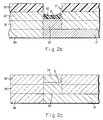
- the metal-1 lines 21, low temperature oxide layer 20 and metal plug 23 are formed in a conventional manner, and then a third low temperature oxide layer 20′ is deposited over the low temperature oxide layer 20 and metal plug 23.
- the metal-1 lines 21 have a thickness the order of 0.65 microns.
- the low temperature oxide layer 20 typically has a thickness of about 1.0 micron.
- the metal plug 23 typically has a thickness of about 1.2 micron.
- a first photoresist layer 30 is deposited over the third oxide layer 20′ and it is masked and etched in a conventional manner to form a trough which defines metal-2 lines which are to be formed.
- the first photoresist layer 30 typically has a thickness of about 1.2 micron, to match the thickness of the metal plug 23.
- a relatively thin adhesion layer 31, or selective metal layer 31, is deposited by means of a sputtering procedure, for example over the etched surface.
- the adhesion layer 31 typically comprises a metal such as titanium tungsten alloy or aluminum alloy, or the like.
- a low viscosity photoresist layer 32 is deposited over the adhesion layer 31 which covers the surfaces and partially fills the trench.
- the low viscosity photoresist layer 32 typically has a thickness of about 3000 Angstroms.
- the integrated circuit 10 is then anisotropically etched in a conventional manner such that the adhesion layer 31 is removed to a point below the edge of the third oxide layer 20′.
- the etching procedure employed is typically an anisotropic dry etching procedure.
- the low viscosity photoresist layer 32 and top-most portion of the adhesion layer 31 are removed during this procedure.
- the circuit 10 may be wet etched in a conventional manner to clean the exposed surfaces. The wet etching step removes the first photoresist layer 30 from the surface of the adhesion layer 31.
- a dip in hydrogen peroxide may be employed to remove the adhesion layer 31 in the area identified by the phantom lined adhesion layer 31′ in Fig. 2b. This ensures that no portion of the adhesion layer protrudes above the oxide layer 20′.
- a preclean treatment may then be performed, if desired using a conventional hydrogen fluoride (100:1) buffer solution, for example.
- second level metal is deposited into the trench by means of a conventional selective metal chemical vapor deposition procedure. This creates selective metal-2 lines 24 on top of the adhesion layer 31. Typically, selective tungsten is used to form the metal-2 lines 24. In addition, other selective metals such as molybdenum, for example, may be employed as the material used as the selective metal-2 lines 24.
- Higher-order metal interconnection lines may also be formed by following the above disclosed procedure.
- the next layer of oxide is deposited over the metal-2 lines 24, and a metal plug is formed therein contacting the metal-2 lines.
- the balance of the processing steps described with reference to Figs. 2a-2c are then performed. As many lines as is required to complete the integrated circuit 10 may be fabricated using the principles of the present invention.
- the metal-2 lines 24 formed in accordance with the principles of the present invention are more electromigration resistant than conventional metal lines.
- the present invention eliminates metal step coverage problems, provides for full planarization of multi-level metal metalization, and provides for self-aligned filling of high aspect ratio contacts, vias and metal grooves.
- the present invention eliminates metal etching steps, and therefore eliminates corrosion and contaminants which result in yield problems.
- the present invention provides for a method of multi-level metal integrated circuit fabrication that eliminates metal step coverage problems, provides for full planarization of multi-level metal metalization, provides for self-aligned filling of high aspect ratio contacts, vias and metal grooves and provides electromigration resistant interconnections.
- the present invention has the advantage of being a simple and practical procedure that produces multi-level integrated circuits.
Landscapes
- Internal Circuitry In Semiconductor Integrated Circuit Devices (AREA)
Claims (8)
- Verfahren zur Herstellung von Metallzwischenverbindungsschichten höherer Ordnung in einer Mehrschichten-Metallhalbleitervorrichtung, welche zumindest eine Metallzwischenverbindungsschicht (21), die auf einer ersten Oxidschicht (18) und in Vias, die in der Oxidschicht (18) gebildet sind, abgeschieden ist, eine zweite Oxidschicht (20), die auf der Metallzwischenverbindungsschicht (21) angeordnet ist, und einen Metallstopfen (23), der in der zweiten Oxidschicht, die mit der Metallzwischenverbindungsschicht verbunden ist, angeordnet ist, aufweist, wobei das Verfahren die Schritte aufweist:
Abscheiden einer dritten Oxidschicht (20′) oberhalb der zweiten Oxidschicht (20) und des Metallstopfens (23);
Abscheiden einer Photolackschicht (30) oberhalb der dritten Oxidschicht (20′), die eine umgekehrte Photolackmaske auf der dritten Oxidschicht mit Gräben darin definiert, die eine Metallzwischenverbindungsschicht höherer Ordnung definiert, wobei zumindest ein Graben oberhalb des Metallstopfens (23) angeordnet ist;
Ätzen über die umgekehrte Photolackmaske zur Bildung der Gräben in der dritten Oxidschicht (20′);
Abscheiden einer Haftschicht (31) oberhalb der Photolackmaske und innerhalb der Gräben, dadurch Bilden einer Grabenlinie, die den Metallstopfen (23) kontaktiert;
Abscheiden einer Photolackschicht (32) geringer Viskosität auf der Haftschicht (30);
anisotropes Ätzen der Haftschicht (31) und der Photolackschicht (32) geringer Viskosität beginnend von der oberen Oberfläche des Photolackes (30) und von den Gräben zur Sicherstellunng, daß kein Abschnitt der Schicht (32) geringer Viskosität und der Haftschicht (31) oberhalb der dritten Oxidschicht (20′) auf den Grabenseitenwänden hervorsteht;
Entfernen der verbleibenden Photolackschicht geringer Viskosität, um die Haftschicht freizulegen;
und Abscheiden von selektivem Metall oberhalb der Haftschicht zur Bildung der Metallzwischenverbindungsschicht höherer Ordnung. - Verfahren nach Anspruch 1, welches des weiteren den Schritt aufweist:
Naßätzen der anisotrop geätzten Haftschicht (31) und der Photolackschicht (32) geringer Viskosität aufeinanderfolgend, um die Oberfläche der Haftschicht (31) zu reinigen. - Verfahren nach Anspruch 1 oder 2, bei dem der Schritt des Abscheidens der Haftschicht (31) den Schritt aufweist:
Abscheiden einer Haftschicht, welche eine Titan-Wolfram-Legierung aufweist. - Verfahren nach Anspruch 1 oder 2, bei dem der Schritt des Abscheidens der Haftschicht den Schritt aufweist:
Abscheiden einer Haftschicht, welche eine Aluminium-Legierung aufweist. - Verfahren nach Anspruch 1, 2 oder 3, bei dem der Schritt des Abscheidens der Haftschicht den Schritt aufweist:
Sputtern einer Haftschicht, welche eine Titan-Wolfram-Legierung aufweist. - Verfahren nach Anspruch 1, 2 oder 4, bei dem der Schritt des Abscheidens der Haftschicht den Schritt aufweist:
Sputtern einer Haftschicht, welche eine Aluminium-Legierung aufweist. - Verfahren nach einem der vorhergehenden Ansprüche, bei dem der Schritt des Abscheidens des selektiven Metalls oberhalb der Haftschicht den Schritt aufweist:
chemisches Dampf-Abscheiden von selektivem Wolfram oberhalb der Haftschicht. - Verfahren nach einem der vorhergehenden Ansprüche, bei dem der Schritt des Abscheidens von selektivem Metall oberhalb der Haftschicht den Schritt aufweist:
chemisches Dampf-Abscheiden von Molybdän oberhalb der Haftschicht.
Applications Claiming Priority (3)
| Application Number | Priority Date | Filing Date | Title |
|---|---|---|---|
| US338681 | 1989-04-17 | ||
| US07/338,681 US4961822A (en) | 1989-04-17 | 1989-04-17 | Fully recessed interconnection scheme with titanium-tungsten and selective CVD tungsten |
| PCT/US1990/001283 WO1990013142A1 (en) | 1989-04-17 | 1990-03-12 | Fully recessed interconnection scheme with titanium-tungsten and selective cvd tungsten |
Publications (2)
| Publication Number | Publication Date |
|---|---|
| EP0424485A1 EP0424485A1 (de) | 1991-05-02 |
| EP0424485B1 true EP0424485B1 (de) | 1994-12-28 |
Family
ID=23325699
Family Applications (1)
| Application Number | Title | Priority Date | Filing Date |
|---|---|---|---|
| EP90905128A Expired - Lifetime EP0424485B1 (de) | 1989-04-17 | 1990-03-12 | Vollverdiefte verbindungsstruktur mit titanium/wolfram und selektivem cvd-wolfram |
Country Status (6)
| Country | Link |
|---|---|
| US (1) | US4961822A (de) |
| EP (1) | EP0424485B1 (de) |
| JP (1) | JPH0685414B2 (de) |
| KR (1) | KR940001395B1 (de) |
| DE (1) | DE69015564T2 (de) |
| WO (1) | WO1990013142A1 (de) |
Families Citing this family (21)
| Publication number | Priority date | Publication date | Assignee | Title |
|---|---|---|---|---|
| US5093710A (en) * | 1989-07-07 | 1992-03-03 | Seiko Epson Corporation | Semiconductor device having a layer of titanium nitride on the side walls of contact holes and method of fabricating same |
| US5198298A (en) * | 1989-10-24 | 1993-03-30 | Advanced Micro Devices, Inc. | Etch stop layer using polymers |
| JPH0682631B2 (ja) * | 1990-03-16 | 1994-10-19 | 株式会社東芝 | 半導体装置の製造方法 |
| US5030587A (en) * | 1990-06-05 | 1991-07-09 | Micron Technology, Inc. | Method of forming substantially planar digit lines |
| US5244538A (en) * | 1991-07-26 | 1993-09-14 | Microelectronics And Computer Technology Corporation | Method of patterning metal on a substrate using direct-write deposition of a mask |
| US5382315A (en) * | 1991-02-11 | 1995-01-17 | Microelectronics And Computer Technology Corporation | Method of forming etch mask using particle beam deposition |
| JPH04320330A (ja) * | 1991-04-19 | 1992-11-11 | Sharp Corp | 半導体装置のコンタクト部の形成方法 |
| DE69220559T2 (de) * | 1991-12-18 | 1997-12-18 | Sgs Thomson Microelectronics | Verfahren zur Herstellung von Kontakten in Löchern in integrierten Schaltungen |
| US5275973A (en) * | 1993-03-01 | 1994-01-04 | Motorola, Inc. | Method for forming metallization in an integrated circuit |
| US6297110B1 (en) | 1994-07-29 | 2001-10-02 | Stmicroelectronics, Inc. | Method of forming a contact in an integrated circuit |
| US5625231A (en) * | 1995-03-10 | 1997-04-29 | Advanced Micro Devices, Inc. | Low cost solution to high aspect ratio contact/via adhesion layer application for deep sub-half micrometer back-end-of line technology |
| TW381331B (en) * | 1996-06-17 | 2000-02-01 | Winbond Electronic Corp | Manufacturing method for integrated circuit conductive plugs avoiding the generation of voids |
| JP3285509B2 (ja) * | 1997-03-18 | 2002-05-27 | 三菱電機株式会社 | 半導体装置 |
| JP2002093811A (ja) * | 2000-09-11 | 2002-03-29 | Sony Corp | 電極および半導体装置の製造方法 |
| US6383920B1 (en) | 2001-01-10 | 2002-05-07 | International Business Machines Corporation | Process of enclosing via for improved reliability in dual damascene interconnects |
| US6770566B1 (en) | 2002-03-06 | 2004-08-03 | Cypress Semiconductor Corporation | Methods of forming semiconductor structures, and articles and devices formed thereby |
| US6753248B1 (en) * | 2003-01-27 | 2004-06-22 | Applied Materials, Inc. | Post metal barrier/adhesion film |
| KR101061296B1 (ko) * | 2010-07-01 | 2011-08-31 | 주식회사 하이닉스반도체 | 반도체 소자 및 그 형성 방법 |
| TWI403235B (zh) * | 2010-07-14 | 2013-07-21 | 台灣創新記憶體股份有限公司 | 埋藏式電路結構之製作方法 |
| US8772155B2 (en) | 2010-11-18 | 2014-07-08 | Micron Technology, Inc. | Filling cavities in semiconductor structures having adhesion promoting layer in the cavities |
| US8859417B2 (en) | 2013-01-03 | 2014-10-14 | Globalfoundries Inc. | Gate electrode(s) and contact structure(s), and methods of fabrication thereof |
Family Cites Families (13)
| Publication number | Priority date | Publication date | Assignee | Title |
|---|---|---|---|---|
| JPS5815250A (ja) * | 1981-07-21 | 1983-01-28 | Fujitsu Ltd | 半導体装置の製造方法 |
| FR2566181B1 (fr) * | 1984-06-14 | 1986-08-22 | Commissariat Energie Atomique | Procede d'autopositionnement d'une ligne d'interconnexion sur un trou de contact electrique d'un circuit integre |
| US4708767A (en) * | 1984-10-05 | 1987-11-24 | Signetics Corporation | Method for providing a semiconductor device with planarized contacts |
| DE3650077T2 (de) * | 1985-03-15 | 1995-02-23 | Hewlett Packard Co | Metallisches Verbindungssystem mit einer ebenen Fläche. |
| US4666737A (en) * | 1986-02-11 | 1987-05-19 | Harris Corporation | Via metallization using metal fillets |
| KR910006975B1 (ko) * | 1986-12-19 | 1991-09-14 | 휴우즈 에어크라프트 캄파니 | 도전성 플러그로 집적 회로 상의 접점 및 비아를 충전하는 방법 |
| JPH0670999B2 (ja) * | 1986-12-27 | 1994-09-07 | 日本電気株式会社 | 半導体装置の層間接続方法 |
| JPS63257268A (ja) * | 1987-04-14 | 1988-10-25 | Nec Corp | 半導体集積回路 |
| US4808545A (en) * | 1987-04-20 | 1989-02-28 | International Business Machines Corporation | High speed GaAs MESFET having refractory contacts and a self-aligned cold gate fabrication process |
| JPS6441240A (en) * | 1987-08-07 | 1989-02-13 | Nec Corp | Semiconductor integrated circuit device |
| JPS6455861A (en) * | 1987-08-27 | 1989-03-02 | Mitsubishi Electric Corp | Semiconductor device |
| JPH01225336A (ja) * | 1988-03-04 | 1989-09-08 | Mitsubishi Electric Corp | 半導体装置の製造方法 |
| JPH0234957A (ja) * | 1988-07-25 | 1990-02-05 | Matsushita Electron Corp | 半導体装置の製造方法 |
-
1989
- 1989-04-17 US US07/338,681 patent/US4961822A/en not_active Expired - Fee Related
-
1990
- 1990-03-12 DE DE69015564T patent/DE69015564T2/de not_active Expired - Fee Related
- 1990-03-12 KR KR1019900702631A patent/KR940001395B1/ko not_active Expired - Fee Related
- 1990-03-12 WO PCT/US1990/001283 patent/WO1990013142A1/en not_active Ceased
- 1990-03-12 JP JP2505072A patent/JPH0685414B2/ja not_active Expired - Lifetime
- 1990-03-12 EP EP90905128A patent/EP0424485B1/de not_active Expired - Lifetime
Also Published As
| Publication number | Publication date |
|---|---|
| JPH03505507A (ja) | 1991-11-28 |
| DE69015564T2 (de) | 1995-08-10 |
| KR920700475A (ko) | 1992-02-19 |
| WO1990013142A1 (en) | 1990-11-01 |
| JPH0685414B2 (ja) | 1994-10-26 |
| EP0424485A1 (de) | 1991-05-02 |
| US4961822A (en) | 1990-10-09 |
| DE69015564D1 (de) | 1995-02-09 |
| KR940001395B1 (ko) | 1994-02-21 |
Similar Documents
| Publication | Publication Date | Title |
|---|---|---|
| EP0424485B1 (de) | Vollverdiefte verbindungsstruktur mit titanium/wolfram und selektivem cvd-wolfram | |
| US5795823A (en) | Self aligned via dual damascene | |
| US6090700A (en) | Metallization method for forming interconnects in an integrated circuit | |
| EP0435388B1 (de) | Verfahren zum teilweisen Anfüllen von Kontakten oder Durchführungen verschiedener Tiefe | |
| US6352917B1 (en) | Reversed damascene process for multiple level metal interconnects | |
| US6011311A (en) | Multilevel interconnect structure for integrated circuits | |
| US6180531B1 (en) | Semiconductor manufacturing method | |
| US5227335A (en) | Tungsten metallization | |
| JP2587857B2 (ja) | 埋込み多重レベル間相互接続体装置 | |
| US5504038A (en) | Method for selective tungsten sidewall and bottom contact formation | |
| KR20060015515A (ko) | 멀티레벨 상호접속 구조를 제조하기 위한 방법 | |
| JPH10189733A (ja) | 多孔性誘電体の金属被覆法 | |
| US5429987A (en) | Method for profile control of selective metallization | |
| US6939812B2 (en) | Method of forming an etch stop layer in a semiconductor device | |
| US5801096A (en) | Self-aligned tungsen etch back process to minimize seams in tungsten plugs | |
| US6027994A (en) | Method to fabricate a dual metal-damascene structure in a substrate | |
| KR100342639B1 (ko) | 반도체 구조물의 제조 방법 | |
| EP0665589B1 (de) | Herstellungsverfahren für eine integrierte Halbleiterschaltung mit einem Verbundungsleiter, der in einer Schutzschicht auf der integriertere Halbleiterschaltung eingebettet ist | |
| US5607878A (en) | Contact plug forming method | |
| US6277739B1 (en) | Method of forming a barrier layer underlying a tungsten plug structure in a high aspect ratio contact hole | |
| EP0324198B1 (de) | Verfahren zum Herstellen von elektrischen Kontakten in integrierten Schaltungen | |
| WO1991010261A1 (en) | Semiconductor interconnect structure utilizing a polyimide insulator | |
| US6340638B1 (en) | Method for forming a passivation layer on copper conductive elements | |
| KR100340860B1 (ko) | 반도체 소자의 콘택 플러그 제조 방법 | |
| KR100338092B1 (ko) | 반도체소자의제조방법 |
Legal Events
| Date | Code | Title | Description |
|---|---|---|---|
| PUAI | Public reference made under article 153(3) epc to a published international application that has entered the european phase |
Free format text: ORIGINAL CODE: 0009012 |
|
| AK | Designated contracting states |
Kind code of ref document: A1 Designated state(s): DE FR GB |
|
| 17P | Request for examination filed |
Effective date: 19910502 |
|
| 17Q | First examination report despatched |
Effective date: 19930118 |
|
| GRAA | (expected) grant |
Free format text: ORIGINAL CODE: 0009210 |
|
| REF | Corresponds to: |
Ref document number: 69015564 Country of ref document: DE Date of ref document: 19950209 |
|
| ET | Fr: translation filed | ||
| PLBE | No opposition filed within time limit |
Free format text: ORIGINAL CODE: 0009261 |
|
| STAA | Information on the status of an ep patent application or granted ep patent |
Free format text: STATUS: NO OPPOSITION FILED WITHIN TIME LIMIT |
|
| 26N | No opposition filed | ||
| REG | Reference to a national code |
Ref country code: GB Ref legal event code: 732E |
|
| REG | Reference to a national code |
Ref country code: FR Ref legal event code: TP Ref country code: FR Ref legal event code: CD Ref country code: FR Ref legal event code: CA |
|
| REG | Reference to a national code |
Ref country code: GB Ref legal event code: IF02 |
|
| PGFP | Annual fee paid to national office [announced via postgrant information from national office to epo] |
Ref country code: FR Payment date: 20020211 Year of fee payment: 13 |
|
| PGFP | Annual fee paid to national office [announced via postgrant information from national office to epo] |
Ref country code: GB Payment date: 20020220 Year of fee payment: 13 |
|
| PGFP | Annual fee paid to national office [announced via postgrant information from national office to epo] |
Ref country code: DE Payment date: 20020221 Year of fee payment: 13 |
|
| PG25 | Lapsed in a contracting state [announced via postgrant information from national office to epo] |
Ref country code: GB Free format text: LAPSE BECAUSE OF NON-PAYMENT OF DUE FEES Effective date: 20030312 |
|
| PG25 | Lapsed in a contracting state [announced via postgrant information from national office to epo] |
Ref country code: DE Free format text: LAPSE BECAUSE OF NON-PAYMENT OF DUE FEES Effective date: 20031001 |
|
| GBPC | Gb: european patent ceased through non-payment of renewal fee |
Effective date: 20030312 |
|
| PG25 | Lapsed in a contracting state [announced via postgrant information from national office to epo] |
Ref country code: FR Free format text: LAPSE BECAUSE OF NON-PAYMENT OF DUE FEES Effective date: 20031127 |
|
| REG | Reference to a national code |
Ref country code: FR Ref legal event code: ST |