EP0424838A2 - Arithmetische Schaltung zur Berechnung und Akkumulation von Absolutwerten der Differenz zwischen zwei numerischen Werten - Google Patents
Arithmetische Schaltung zur Berechnung und Akkumulation von Absolutwerten der Differenz zwischen zwei numerischen Werten Download PDFInfo
- Publication number
- EP0424838A2 EP0424838A2 EP90120197A EP90120197A EP0424838A2 EP 0424838 A2 EP0424838 A2 EP 0424838A2 EP 90120197 A EP90120197 A EP 90120197A EP 90120197 A EP90120197 A EP 90120197A EP 0424838 A2 EP0424838 A2 EP 0424838A2
- Authority
- EP
- European Patent Office
- Prior art keywords
- addition result
- value
- result
- inverted
- sum
- Prior art date
- Legal status (The legal status is an assumption and is not a legal conclusion. Google has not performed a legal analysis and makes no representation as to the accuracy of the status listed.)
- Withdrawn
Links
Images


Classifications
-
- G—PHYSICS
- G06—COMPUTING OR CALCULATING; COUNTING
- G06F—ELECTRIC DIGITAL DATA PROCESSING
- G06F7/00—Methods or arrangements for processing data by operating upon the order or content of the data handled
- G06F7/38—Methods or arrangements for performing computations using exclusively denominational number representation, e.g. using binary, ternary, decimal representation
- G06F7/48—Methods or arrangements for performing computations using exclusively denominational number representation, e.g. using binary, ternary, decimal representation using non-contact-making devices, e.g. tube, solid state device; using unspecified devices
- G06F7/544—Methods or arrangements for performing computations using exclusively denominational number representation, e.g. using binary, ternary, decimal representation using non-contact-making devices, e.g. tube, solid state device; using unspecified devices for evaluating functions by calculation
-
- G—PHYSICS
- G06—COMPUTING OR CALCULATING; COUNTING
- G06F—ELECTRIC DIGITAL DATA PROCESSING
- G06F2207/00—Indexing scheme relating to methods or arrangements for processing data by operating upon the order or content of the data handled
- G06F2207/544—Indexing scheme relating to group G06F7/544
- G06F2207/5442—Absolute difference
Definitions
- the present invention relates to an arithmetic circuit and, more particularly, to an arithmetic circuit for calculating and accumulating the absolute values of the difference between two numerical values.
- Calculating and accumulating the absolute values of the difference between two numerical values is commonly practiced to, for example, search for an optimum block in the event of coding a video signal using motion compensation.
- An arithmetic circuit for implementing this kind of operation has customarily been made up of an absolute value calculating section and an accumulating section.
- the absolute v-lue calculating section or calculator inverts one of two n-bit numerical values represented by 2's compliment notation, adds the inverted numerical value to the other numerical value, and processes the sum on the basis of the sign so as to produce the absolute value of the difference.
- the accumulating section or accumulator sequentially accumulates the resulting absolute values of the difference.
- the absolute value calculator may be implemented with an absolute value calculating circuit which is disclosed in European patent application EP 0328063 A2 laid open for public inspection on August 16, 1989.
- the accumulator may be constituted by the combination of an adder and a delay circuit.
- Such a conventional arithmetic circuit is advantageous in that the absolute value calculator needs only a single adder.
- the conventional circuit cannot avoid large circuit scale which not only slows down the operation due to the delay in data propagation but also aggravates power consumption.
- a first adder produces a sum of the first numerical value and inverted value and outputs the sum as a first addition result.
- a second inverter inverts the first addition result to output an inverted addition result.
- a selector selects either one of the inverted addition result and first addition result on the basis of the sign of the first addition result and outputs the one result as a selected value.
- a correcting value generating circuit outputs a correcting value on the basis of the sign of the first addition result.
- a second adder produces a sum of the selected value, the correcting value and a delayed addition result and outputs the sum as a second addition result.
- a first delay circuit delays the second addition result by a predetermined delay to produce the delayed addition result while outputting the delayed addition result as the operation result.
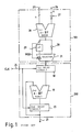
- the prior art arithmetic circuit has an absolute value calculator 100 and an accumulator 200.
- the absolute value calculator 100 is constructed and arranged as taught in previously mentioned European application.
- Fig. 1 two numerical values x and y represented by 2's complement notation and having the same predetermined bit length, e.g., n bits, are applied to input terminals 25 and 26.
- the numerical value x is directly fed to a first n-bit adder 28 while the numerical value y is fed to the adder 28 via a first inverter 27.
- the numerical value x and the inverted numerical value y from the first inverter 27 are added, x + y , by the first adder 28.
- the value (x - y - 1) is delivered to a second inverter 30 and an increment circuit 29 while the most significant bit (MSB) indicative of the sign of the value is fed to a select terminal of a selector 31.
- the second inverter 30 inverts (x - y - 1) to produce an output (y - x).
- a first delay circuit 18 delays the output of the selector 31, i.e., the absolute value
- the second adder 19 adds the delayed absoulte value from the first delay circuit 18 to an accumulated value from a second delay circuit 20, the resulting sum being fed to the delay circuit 20.
- the second delay circuit 20 delays the sum fed thereto from the adder 19 by one clock and feeds the delayed sum via an output terminal 21 as an operation result while delivering it to the second adder 19. Such a procedure is repeated to accumulate the absolute values of the difference.
- a problem with the circuitry of Fig. 1 is that the operation speed is low and the power consumption is great, as stated earlier.
- the arithmetic circuit has an absolute value calculating section or calculator 300 and an accumulating section or accumulator 400.
- the absolute value calculator 300 is made up of a first and a second inverter 1 and 3, a first adder 2, and a selector 4.
- the accumulator 400 is constituted by a first to a third delay circuit 5, 6 and 9, a second adder 7, and a third inverter 8.
- the first result is fed on one hand directly to the selector 4 and on the other hand to the selector 4 via the second inverter 3.
- MSB of the first addition result, or sum is delivered to the select terminal of the selector 4 and the second delay circuit 6.
- the selector 4 selects either one of the two inputs depending on the value of MSB, i.e., the sign of (x - y - 1), as in the prior art circuitry. Specifically, if MSB is ONE, the selector 4 selects the output of the second inverter 3 since x - y - 1 ⁇ 0. Conversely, if MSB is ZERO, the selector 4 selects non-inverted (x - y - 1) since x - y ⁇ 0.
- the illustrative embodiment does not include the conventional increment circuit, so that the output of the selector 4 is (x - y -1) when MSB is ZERO. This particular embodiment assigns the role of the increment circuit 29, Fig.
- the absolute value outputted by the selector 4 is delayed by the first delay circuit 5 by one period of a clock signal which is applied to a clock input terminal 24.
- the delayed absolute value is fed to the second adder 7.
- MSB of the output (x - y - 1) of the first adder 2 is delayed by the second delay circuit 6 by one clock and then fed out as delayed MSB.
- the third inverter 8 inverts the delayed MSB and feeds the inverted delayed MSB to the carry input terminal CY of the second adder 7.
- the second adder 7 adds the delayed absolute value from the first delay circuit 5, the immediately preceding accumulation result fed from the third delay circuit 9, and the value applied to the carry input terminal CY.
- the delay circuit 9 has the same construction and function as the second delay circuit 20, Fig. 1.
- the delay circuit 9 delays the second addition result from the second adder 7 by one period of the clock signal and feeds the delayed sum to the second adder 7 as an immediately preceding result of accumulation while feeding it out as an operation result via an output terminal 10.
- the result of operation is outputted via the third delay circuit 9 and not directly from the second adder 7, as shown and described. This is to synchronize the operation result to the clock signal.
- the illustrative embodiment implements the same function as the prior art circuity of Fig. 1.
- Fig. 3 shows an alternative embodiment of the present invention which is essentially the same in construction and operation as the previous embodiment except for an accumulator 500.
- the accumulator 500 shown in Fig. 3 does not have the first and the second delay circuits of Fig. 2.
- the first and second delay circuits 5 and 6 of the previous embodiment serve to match the speeds of the outputs of the selector 4 and third delay circuit 9 by considering the low operation speed of the second adder 7.
- Such speed matching delay circuits are omissible if the second adder 7 is implemented with a bipolar element or similar element operable at high speed.
- the present invention provides an arithmetic circuit which eliminates the need for the conventional increment circuit by inverting MSB of the output of a first adder and feeding the inverted MSB to the carry input of a second adder.
- the serial connection of the first adder and increment circuit is omitted to enhance high speed arithmetic operations, miniature circuit arrangement, and cut-down of power consumption.
Landscapes
- Engineering & Computer Science (AREA)
- Physics & Mathematics (AREA)
- General Physics & Mathematics (AREA)
- Theoretical Computer Science (AREA)
- Computational Mathematics (AREA)
- Computing Systems (AREA)
- Mathematical Analysis (AREA)
- Mathematical Optimization (AREA)
- Pure & Applied Mathematics (AREA)
- General Engineering & Computer Science (AREA)
- Complex Calculations (AREA)
Applications Claiming Priority (2)
| Application Number | Priority Date | Filing Date | Title |
|---|---|---|---|
| JP1276872A JPH03136166A (ja) | 1989-10-23 | 1989-10-23 | 演算回路 |
| JP276872/89 | 1989-10-23 |
Publications (2)
| Publication Number | Publication Date |
|---|---|
| EP0424838A2 true EP0424838A2 (de) | 1991-05-02 |
| EP0424838A3 EP0424838A3 (en) | 1992-09-02 |
Family
ID=17575585
Family Applications (1)
| Application Number | Title | Priority Date | Filing Date |
|---|---|---|---|
| EP19900120197 Withdrawn EP0424838A3 (en) | 1989-10-23 | 1990-10-22 | Arithmetic circuit for calculating and accumulating absolute values of the difference between two numerical values |
Country Status (4)
| Country | Link |
|---|---|
| US (1) | US5040136A (de) |
| EP (1) | EP0424838A3 (de) |
| JP (1) | JPH03136166A (de) |
| CA (1) | CA2028230C (de) |
Cited By (1)
| Publication number | Priority date | Publication date | Assignee | Title |
|---|---|---|---|---|
| RU2112271C1 (ru) * | 1996-12-17 | 1998-05-27 | Игорь Олегович Анишкин | Устройство для вычисления функции близости текущих и эталонных признаков объектов с адаптацией к условиям обстановки |
Families Citing this family (6)
| Publication number | Priority date | Publication date | Assignee | Title |
|---|---|---|---|---|
| JP3304971B2 (ja) * | 1990-07-23 | 2002-07-22 | 沖電気工業株式会社 | 絶対値演算回路 |
| JP2601960B2 (ja) * | 1990-11-15 | 1997-04-23 | インターナショナル・ビジネス・マシーンズ・コーポレイション | データ処理方法及びその装置 |
| JPH05216624A (ja) * | 1992-02-03 | 1993-08-27 | Mitsubishi Electric Corp | 演算装置 |
| US5610850A (en) * | 1992-06-01 | 1997-03-11 | Sharp Kabushiki Kaisha | Absolute difference accumulator circuit |
| US5563813A (en) * | 1994-06-01 | 1996-10-08 | Industrial Technology Research Institute | Area/time-efficient motion estimation micro core |
| US6377970B1 (en) * | 1998-03-31 | 2002-04-23 | Intel Corporation | Method and apparatus for computing a sum of packed data elements using SIMD multiply circuitry |
Family Cites Families (7)
| Publication number | Priority date | Publication date | Assignee | Title |
|---|---|---|---|---|
| US3829671A (en) * | 1973-04-25 | 1974-08-13 | Westinghouse Electric Corp | Method and circuit for calculating the square root of the sum of two squares |
| JPS61214025A (ja) * | 1985-03-20 | 1986-09-22 | Mitsubishi Electric Corp | 差の絶対値比較回路 |
| CA1257003A (en) * | 1985-06-19 | 1989-07-04 | Tadayoshi Enomoto | Arithmetic circuit |
| US4825400A (en) * | 1986-01-13 | 1989-04-25 | General Electric Company | Floating point accumulator circuit |
| JPH0650462B2 (ja) * | 1986-02-18 | 1994-06-29 | 日本電気株式会社 | シフト数制御回路 |
| JPS6395533A (ja) * | 1986-10-09 | 1988-04-26 | Mitsubishi Electric Corp | 論理回路 |
| JPH01204138A (ja) * | 1988-02-09 | 1989-08-16 | Nec Corp | 演算回路 |
-
1989
- 1989-10-23 JP JP1276872A patent/JPH03136166A/ja active Pending
-
1990
- 1990-10-22 EP EP19900120197 patent/EP0424838A3/en not_active Withdrawn
- 1990-10-22 CA CA002028230A patent/CA2028230C/en not_active Expired - Fee Related
- 1990-10-23 US US07/601,628 patent/US5040136A/en not_active Expired - Fee Related
Cited By (1)
| Publication number | Priority date | Publication date | Assignee | Title |
|---|---|---|---|---|
| RU2112271C1 (ru) * | 1996-12-17 | 1998-05-27 | Игорь Олегович Анишкин | Устройство для вычисления функции близости текущих и эталонных признаков объектов с адаптацией к условиям обстановки |
Also Published As
| Publication number | Publication date |
|---|---|
| CA2028230C (en) | 1994-07-05 |
| EP0424838A3 (en) | 1992-09-02 |
| CA2028230A1 (en) | 1991-04-24 |
| JPH03136166A (ja) | 1991-06-10 |
| US5040136A (en) | 1991-08-13 |
Similar Documents
| Publication | Publication Date | Title |
|---|---|---|
| EP0161089B1 (de) | Multiplizierer mit doppelter Genauigkeit | |
| US6069487A (en) | Programmable logic device circuitry for improving multiplier speed and/or efficiency | |
| US4953115A (en) | Absolute value calculating circuit having a single adder | |
| EP0007729B1 (de) | Digitales, Mittelwert bildendes TiefpaBfilter und Verfahren zum Herausfiltern einer niederfrequenten Komponente aus einer zusammengesetzten Wellenform | |
| EP0146963A2 (de) | Rekursives digitales Filter | |
| EP0372566A2 (de) | Arithmetische Reziprokwertschaltung mit Festwertspeichertabelle | |
| EP0424838A2 (de) | Arithmetische Schaltung zur Berechnung und Akkumulation von Absolutwerten der Differenz zwischen zwei numerischen Werten | |
| KR100302093B1 (ko) | 교차형디지탈유한임펄스응답필터에서이진입력신호를탭계수와승산시키는방법및회로배열과교차형디지탈필터의설계방법 | |
| EP0168787A2 (de) | Abrundungseinheit zum Gebrauch bei der arithmetischen Verarbeitung von Gleitkommadaten | |
| EP0164451B1 (de) | Arithmetische Verarbeitungseinheit zum Ausführen einer Gleitkommaoperation | |
| US5177703A (en) | Division circuit using higher radices | |
| JPH0640301B2 (ja) | 並列乗算回路 | |
| EP0312370B1 (de) | Digitaloszillator | |
| EP0637797A1 (de) | Kalkulationsgerät | |
| US6127863A (en) | Efficient fractional divider | |
| TW425526B (en) | Carry increment adder using clock phase | |
| EP0304841B1 (de) | Bit-serielle Integratorschaltung | |
| EP0281094A2 (de) | Zähler | |
| EP0479562A2 (de) | Berechnungsverfahren für Gleitkommadaten | |
| JPH0519170B2 (de) | ||
| US6542539B1 (en) | Multiported register file for coefficient use in filters | |
| JP2629737B2 (ja) | アキュムレータ | |
| JPH06152330A (ja) | ディジタルフィルター | |
| KR940007925B1 (ko) | 부호처리 기능을 가진 누산기 | |
| US5615141A (en) | Multiplying apparatus |
Legal Events
| Date | Code | Title | Description |
|---|---|---|---|
| PUAI | Public reference made under article 153(3) epc to a published international application that has entered the european phase |
Free format text: ORIGINAL CODE: 0009012 |
|
| 17P | Request for examination filed |
Effective date: 19901120 |
|
| AK | Designated contracting states |
Kind code of ref document: A2 Designated state(s): DE FR GB |
|
| PUAL | Search report despatched |
Free format text: ORIGINAL CODE: 0009013 |
|
| AK | Designated contracting states |
Kind code of ref document: A3 Designated state(s): DE FR GB |
|
| 17Q | First examination report despatched |
Effective date: 19950804 |
|
| STAA | Information on the status of an ep patent application or granted ep patent |
Free format text: STATUS: THE APPLICATION IS DEEMED TO BE WITHDRAWN |
|
| 18D | Application deemed to be withdrawn |
Effective date: 19960416 |