EP0007729B1 - Digitales, Mittelwert bildendes TiefpaBfilter und Verfahren zum Herausfiltern einer niederfrequenten Komponente aus einer zusammengesetzten Wellenform - Google Patents
Digitales, Mittelwert bildendes TiefpaBfilter und Verfahren zum Herausfiltern einer niederfrequenten Komponente aus einer zusammengesetzten Wellenform Download PDFInfo
- Publication number
- EP0007729B1 EP0007729B1 EP79301328A EP79301328A EP0007729B1 EP 0007729 B1 EP0007729 B1 EP 0007729B1 EP 79301328 A EP79301328 A EP 79301328A EP 79301328 A EP79301328 A EP 79301328A EP 0007729 B1 EP0007729 B1 EP 0007729B1
- Authority
- EP
- European Patent Office
- Prior art keywords
- digital
- during
- sample
- analog
- signal
- Prior art date
- Legal status (The legal status is an assumption and is not a legal conclusion. Google has not performed a legal analysis and makes no representation as to the accuracy of the status listed.)
- Expired
Links
Images

Classifications
-
- G—PHYSICS
- G06—COMPUTING OR CALCULATING; COUNTING
- G06F—ELECTRIC DIGITAL DATA PROCESSING
- G06F17/00—Digital computing or data processing equipment or methods, specially adapted for specific functions
- G06F17/10—Complex mathematical operations
- G06F17/18—Complex mathematical operations for evaluating statistical data, e.g. average values, frequency distributions, probability functions, regression analysis
-
- H—ELECTRICITY
- H03—ELECTRONIC CIRCUITRY
- H03H—IMPEDANCE NETWORKS, e.g. RESONANT CIRCUITS; RESONATORS
- H03H17/00—Networks using digital techniques
- H03H17/02—Frequency selective networks
- H03H17/04—Recursive filters
Definitions
- This invention relates generally to low pass filters and more particularly to a low pass filter and a method employing analog to digital conversion and digital averaging techniques.
- Low pass filters for recovering low frequency components of a signal spectrum are well known in the art.
- Analog techniques utilizing linear R-C networks are often employed to filter an analog signal.
- R-C networks do not lend themselves to practical implementation with complex IC technology.
- the stability of linear filters is a function of the resistor and capacitor component parameters, which may vary with age and temperature and which vary from one component to another, thereby requiring alignment in the factory.
- linear R-C type filters are not ideal filters in that the signal passed by such a filter includes small contributions from signals received in the past.
- Digital filtering techniques have also been used in the past, but these techniques often require high speed multipliers, shift registers, read-only memories (ROM's), and a plurality of adders. These prior art digital filters require large amounts of chip area when fabricated as an integrated circuit, thereby reducing wafer yields and resulting in higher cost.
- U.S. Patent No. 3,487,405 describes a radar system density zone suppressor having two multistage registers, three adders, four subtractors, two dividers, one multiplier, two accumulators, and one comparator.
- the suppressor averages a succession of digital inputs for modifying amplitudes of video signals applied to a radar screen.
- An object of the present invention is to provide a low pass filter which may easily be implemented within an integrated circuit.
- a low pass averaging filter for providing a low frequency component of an analog input signal, including an analog to digital converter having an input terminal for receiving the analog input signal and having output terminals for providing a digital representation of the received analog input signal; timing circuitry for providing at least one timing signal which defines sequential sample periods; storage circuitry responsive to the at least one timing signal for storing an average digital signal during each sample period; and a sample register in the form of delay circuitry coupled to the analog to digital converter and responsive to the at least one timing signal for storing a digital representation provided by the output terminals during a present sample period and for providing the stored digital representation as an output digital signal during a sample period which occurs a predetermined number of sample periods subsequent to the present sample period characterised by an arithmetic circuit having a multiplexer and an adder- subtractor circuit, the multiplexer being for coupling the input digital signal received during the present sample period from the analog to digital converter to the adder-subtractor circuit during a first portion of the present sample period and coup
- a method of recovering a low frequency component of a composite analog waveform including the steps of converting the analog waveform to a digital representation during periodic sample intervals, storing an average digital signal and storing a digital representation provided by the converting step characterised by providing the stored digital representation as a delayed representation a predetermined number of sample intervals following the sample intervals during which the digital representation was stored; and updating the average digital signal during each sample interval, the updating step including the steps of adding the digital representation provided by the converting step to the average digital signal and subtracting the delayed representation from the average digital signal.
- an analog to digital converter receives an analog input signal and is a source of the input digital signals.
- the running average of the input digital signals corresponds to the low frequency component of the analog signal received by the digital to analog converter.
- Fig. 1 illustrates a low pass digital averaging filter according to a preferred embodiment of the invention.
- An analog to digital converter 2 has an input terminal 4 for receiving a composite analog input signal.
- the output of analog to digital converter 2 is coupled to node 6, and node 6 is coupled to conductors 8 and 10.
- the output of analog to digital converter 2 consists of a plurality of binary bits, each of which is typically associated with a particular binary weighting so that the plurality of binary bits corresponds to the magnitude of the received analog signal.
- the output of the analog to digital converter 2 may also include a sign bit for indicating positive and negative magnitudes.
- conductors 8 and 10 are shown as single lines in Fig. 1.
- Analog to digital converters are well known in the art and will not be further described herein. For a more detailed description of analog to digital conversion, see Digital Electronics with Engineering Applications by Sifferlen and Vartanian, Prentiss-Hall Inc., 1970.
- Conductor 10 couples the output of analog to digital converter 2 to the input of sample register 12.
- sample register 12 is a shift register having a predetermined number of storage locations for storing a predetermined number of digital words. Each of the stored digital words has as many binary bits as are provided by the output of analog to digital converter 2.
- Sample register 12 has an output coupled to conductor 14.
- a timing signal or clock, T I is coupled to sample register 12 by conductor 16.
- Timing signal T is pulsed at a periodic rate so as to define a plurality of sample periods.
- timing signal T is pulsed, and the digital signal currently being output by analog to digital converter 2 is shifted into sample register 12 via conductor 10. If it is assumed that sample register 12 contains eight storage locations, for example, then sample register 12 will be filled with eight digital values after the first eight sample periods.
- timing signal T will again be pulsed, and a new digital value will be shifted into sample register 12. Simultaneously the digital value shifted into sample register 12 during the first sample period will be shifted out onto conductor 14 as an output value.
- sample register 12 acts as a delay element to provide the digital value received eight sample periods prior to the present sample period.
- sample register 12 has been characterized in this preferred embodiment as a shift register, it will be obvious to those skilled in the art that various other storage means may be used to implement sample register 12.
- Conductors 8 and 14 are coupled to first and second inputs, respectively, of adder/subtractor block 18.
- Adder/subtractor block 18 is coupled to storage register 20 by conductor 22.
- conductor 22 symbolizes a group of conductors sufficient to transmit a digital value having a number of binary bits corresponding to the number of binary bits provided by the output of analog to digital converter 2.
- Timing signal T 2 is coupled to storage register 20 by conductor 24 and, when pulsed, causes storage register 20 to store the digital value presented by conductor 22.
- Storage register 20 provides an output coupled to conductor 26 for providing the digital value currently being stored.
- the output of storage register 20 is also coupled to output terminal 28 such that other circuitry (not shown) can access the digital value being stored by storage register 20.
- the output of storage register 20 is fed back by conductor 26 to a third input of adder/subtractor block 1 8.
- sample register 12 contains eight storage locations for storing eight digital values, it being understood that the number eight is chosen only as an example.
- Sample register 12 is initialized to contain eight digital values, each equal to a zero value, and storage register 20 is initialized to contain a zero value.
- timing signal T is pulsed, and the first digital value is shifted into sample register 12.
- a zero value is shifted out of sample register 12 onto conductor 14.
- Adder/ subtractor block 18 adds the first digital value presented by conductor 8 to the zero vaiue presented by conductor 26 and subtracts the zero value presented by conductor 14 such that the output provided to conductor 22 is equal to the digital value provided by conductor 8.
- Timing signal T 2 is then pulsed, and storage register 20 stores this initial digital value.
- a second digital value is output by analog to digital converter 2 and timing signal T 1 is again pulsed so as to shift this second digital value into sample register 12.
- a zero value is again shifted out onto conductor 14.
- adder/subtractor block 18 adds the second digital value on conductor 8 to the first digital value stored by storage register 20 and presented by conductor 26, and subtracts the zero value provided by conductor 14 such that the output provided to conductor 22 is equal to the sum of the first and second digital values.
- Timing signal T z is then pulsed to store this sum into storage register 20. This sequence of events is repeated up to and including the eighth sample period, after which time storage register 20 contains the sum of the first eight sampled digital values. The sum stored by storage register 20 is thus proportional to the average of the first eight digital values.
- a new digital value is provided by analog to digital converter 2 which is shifted into sample register 12. Simultaneously sample register 12 causes the first digital value which was received during the first sample period to be shifted out onto conductor 14.
- adder/subtractor block 18 adds the new digital value on conductor 8 to the sum previously stored by storage register 20 and provided by conductor 26.
- Adder/subtractor block 18 is also operative to subtract the digital value received during the first sample period such that the output provided to conductor 22 equals the sum of the digital values received during the second through ninth sample periods.
- Timing signal T 2 is again pulsed to store this result in storage register 20.
- the value now stored by storage register 20 is proportional to the average of the digital values received during the most recent eight sample periods. In this manner, storage register 20 maintains a running average of only those digital values received during the most recent eight sample periods.
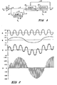
- Waveform A illustrates a high frequency component of a signal and waveform B illustrates a low frequency component of the same signal.
- Waveform C illustrates the composite signal formed by combining the high frequency and low frequency components illustrated in waveforms A and B, respectively.
- the composite analog waveform C is presented to input terminal 4 of analog to digital converter 2 (Fig. 1).
- the points at which the analog composite waveform are sampled by analog to digital converter 2 are indicated by the dots which intersect the composite voltage waveform.
- Waveform D is a plot of the sign and magnitude of the digital value, represented by the direction and length of each line segment, stored by storage register 20 (Fig. 1) during each sample period. It will be appreciated that waveform D effectively recovers the low frequency component shown in waveform B from composite voltage waveform C.
- An adder block 30 receives the previous average digital value stored by storage register 20 via conductor 26 and receives a new digital value from analog to digital converter 2 via conductor 8. The digital values are added and the result of the addition is output on conductor 32 which is coupled to a first input of subtractor block 34. A second input of subtractor 34 is coupled by conductor 14 to the output of the sample register 12. Subtractor block 34 causes the digital value presented by conductor 14 to be subtracted from the digital value provided by conductor 32 and provides an output to conductor 22 to allow the result of the subtraction to be stored in storage register 20. As circuitry for implementing adder block 30 and subtractor block 34 is well known in the art, this circuitry will not be further described.
- a second embodiment of adder/ subtractor block 18 is shown in greater detail.
- the embodiment illustrated by Fig. 4 employs a multiplexing technique whereby a first portion of the sample period is used to add the new digital value output from the analog to digital converter to the previously stored average value, and the result of this addition is temporarily stored in storage register 20. During a second portion of the sample period, the output from the sample register 12 is subtracted from the temporarily stored value to form the updated average value, which is then stored in storage register 20.
- Conductor 36 is an add/subtract control line which is a logic "0" level to select the addition operation and which is a logic "1 " level to select the subtraction operation. In this embodiment, it is assumed that digital values are represented in two's-complement notation. Conductor 36 is coupled to the input of inverter 38 which has an output coupled to a first input of logic AND gate 40. A second input of AND gate 40 receives the digital value output by analog to digital converter 2 via conductor 8. It should be realized that in reality there are a plurality of logic gates corresponding to gate 40 corresponding to the number of binary bits output by analog to digital converter 2. A single AND gate 40 is shown for the ease of illustration only.
- the output of AND gate 40 is coupled to a first input of logic OR gate 42 which has a second input coupled to the output of logic AND gate 44.
- Conductor 36 is coupled to a first input of gate 44 while a second input of gate 44 is coupled to the output of inverter gate 46.
- Inverter gate 46 receives at its input the digital value provided by the output of sample register 12 via conductor 14.
- the output of OR gate 42 is coupled by conductor 48 to a first input of adder circuit 50.
- a second input of adder 50 is coupled to conductor 26 which provides the digital value output from the storage register 20.
- Conductor 36 is also coupled to a carry-in C IN input of adder 50 for causing the result of the addition to be incremented.
- the output of adder 50 is coupled by conductor 22 to the input of storage register 20.
- inverter gate 38 When conductor 36 is at a logic "0" level, the output of inverter gate 38 will be a high level and gate 40 will be enabled while gate 44 will be disabled.
- the new digital value provided by conductor 8 will be passed to conductor 48 to be added within adder block 50 with the previously stored average value provided by conductor 26. The result of the addition is not incremented, and the result is temporarily stored in storage register 20.
- Conductor 36 is then switched to a logic "1" level which causes gate 44 to be enabled and gate 40 to be disabled.
- the digital value provided by the sample register is complemented (one's-complement) by inverter 46, and the complemented value is passed to conductor 48 to be added to the value temporarily stored in storage register 20 during the previous portion of the sample period.
- the result of the addition is incremented such that adder circuit 50 adds the two's-complement of the digital value provided from the sample register which is the same as subtracting the digital value provided from the sample register.
- the result of the two's-complement addition is then stored in storage register 20 and corresponds to the updated average value. It will be obvious to those skilled in the art that the order of the addition and subtraction operations can be reversed without materially affecting the performance of the low pass averaging filter.
Landscapes
- Engineering & Computer Science (AREA)
- Physics & Mathematics (AREA)
- Data Mining & Analysis (AREA)
- Mathematical Physics (AREA)
- General Physics & Mathematics (AREA)
- Pure & Applied Mathematics (AREA)
- Mathematical Analysis (AREA)
- Computational Mathematics (AREA)
- Theoretical Computer Science (AREA)
- Mathematical Optimization (AREA)
- Probability & Statistics with Applications (AREA)
- Life Sciences & Earth Sciences (AREA)
- Evolutionary Biology (AREA)
- Operations Research (AREA)
- Bioinformatics & Computational Biology (AREA)
- Computer Hardware Design (AREA)
- Algebra (AREA)
- Databases & Information Systems (AREA)
- Software Systems (AREA)
- General Engineering & Computer Science (AREA)
- Bioinformatics & Cheminformatics (AREA)
- Analogue/Digital Conversion (AREA)
Claims (2)
Applications Claiming Priority (2)
| Application Number | Priority Date | Filing Date | Title |
|---|---|---|---|
| US05/925,719 US4193118A (en) | 1978-07-18 | 1978-07-18 | Low pass digital averaging filter |
| US925719 | 1978-07-18 |
Publications (2)
| Publication Number | Publication Date |
|---|---|
| EP0007729A1 EP0007729A1 (de) | 1980-02-06 |
| EP0007729B1 true EP0007729B1 (de) | 1983-06-08 |
Family
ID=25452132
Family Applications (1)
| Application Number | Title | Priority Date | Filing Date |
|---|---|---|---|
| EP79301328A Expired EP0007729B1 (de) | 1978-07-18 | 1979-07-09 | Digitales, Mittelwert bildendes TiefpaBfilter und Verfahren zum Herausfiltern einer niederfrequenten Komponente aus einer zusammengesetzten Wellenform |
Country Status (5)
| Country | Link |
|---|---|
| US (1) | US4193118A (de) |
| EP (1) | EP0007729B1 (de) |
| DE (1) | DE2965612D1 (de) |
| HK (1) | HK80588A (de) |
| MY (1) | MY8700013A (de) |
Families Citing this family (32)
| Publication number | Priority date | Publication date | Assignee | Title |
|---|---|---|---|---|
| JPS5574467A (en) * | 1978-11-30 | 1980-06-05 | Olympus Optical Co Ltd | Method of eliminating noise from known frequency |
| JPS55116101A (en) * | 1979-03-01 | 1980-09-06 | Nissan Motor Co Ltd | Signal processor |
| US4375081A (en) * | 1980-12-05 | 1983-02-22 | Pencept, Inc. | Multistage digital filtering utilizing several criteria |
| US4388691A (en) * | 1981-01-23 | 1983-06-14 | The Babcock & Wilcox Company | Velocity pressure averaging system |
| US4558275A (en) * | 1981-04-21 | 1985-12-10 | The Superior Electric Company | Line voltage monitor system |
| JPS58200310A (ja) * | 1982-05-17 | 1983-11-21 | Omron Tateisi Electronics Co | 温度調節器 |
| US4606009A (en) * | 1982-08-20 | 1986-08-12 | John Fluke Mfg. Co., Inc. | Step responsive averaging filter |
| WO1984003769A1 (fr) * | 1983-03-18 | 1984-09-27 | Cosmo Instr Co Ltd | Dispositif d'inspection hydraulique de fuite du type a detection de changement de pression |
| JPS59206737A (ja) * | 1983-05-11 | 1984-11-22 | Cosmo Keiki:Kk | 温度補償機能を有する漏洩検査装置 |
| EP0159314A4 (de) * | 1983-09-26 | 1986-07-23 | Exploration Logging Inc | Geräuschsubtrahierender filter. |
| US4642564A (en) * | 1984-06-15 | 1987-02-10 | Cooper Industries, Inc. | Measuring circuit and method for power distribution equipment |
| FR2575308B1 (fr) * | 1984-12-21 | 1989-03-31 | Bendix Electronics Sa | Procede et chaine de traitement du signal analogique de sortie d'un capteur |
| DE3509762A1 (de) * | 1985-03-19 | 1986-09-25 | Battelle-Institut E.V., 6000 Frankfurt | Schaltungsanordnung zur mittelwertbildung |
| US4714929A (en) * | 1986-09-04 | 1987-12-22 | Davidson Eldon F | Digital averaging filter particularly suited for use with air navigation receivers |
| US6930633B1 (en) | 1988-03-22 | 2005-08-16 | Raytheon Company | Adaptive glint reduction method and system |
| US5000319A (en) * | 1989-06-02 | 1991-03-19 | Leon Mermelstein | Negative storage page with lock-in flaps |
| JP2603134B2 (ja) * | 1989-06-06 | 1997-04-23 | 三菱電機株式会社 | 移動平均処理装置 |
| GB2253102A (en) * | 1991-02-21 | 1992-08-26 | C & I Consultants Limited | Analogue signal monitoring unit |
| EP0615638A1 (de) * | 1991-11-26 | 1994-09-21 | Airtouch Communications | Echtzeit-mittelwertbildungsvorrichtung. |
| JPH0738561B2 (ja) * | 1993-02-15 | 1995-04-26 | 日本電気株式会社 | ディジタルフィルタ回路 |
| US5600318A (en) * | 1995-02-28 | 1997-02-04 | Western Atlas International, Inc. | Seismic data acquisition system |
| US5912825A (en) * | 1997-02-27 | 1999-06-15 | Eg&G Instruments, Inc. | Gated base line restorer system |
| US5889511A (en) * | 1997-01-17 | 1999-03-30 | Tritech Microelectronics International, Ltd. | Method and system for noise reduction for digitizing devices |
| US6081822A (en) * | 1998-03-11 | 2000-06-27 | Agilent Technologies, Inc. | Approximating signal power and noise power in a system |
| US6389441B1 (en) | 1999-05-28 | 2002-05-14 | Eastman Kodak Company | Two dimensional moving average filter |
| ATE386925T1 (de) * | 2002-04-23 | 2008-03-15 | Analytica Of Branford Inc | Vorrichtungen und verfahren zur verringerung von kohärentem rauschen in einem digitalen signalmittler |
| US7053808B2 (en) * | 2003-11-26 | 2006-05-30 | Texas Instruments Incorporated | Suppressing digital-to-analog converter (DAC) error |
| JP4838206B2 (ja) * | 2007-07-18 | 2011-12-14 | ラピスセミコンダクタ株式会社 | フィルタ回路および方法 |
| US9125152B2 (en) * | 2011-08-16 | 2015-09-01 | Utc Fire & Security Corporation | Beacon synchronization in wifi based systems |
| JP5966372B2 (ja) * | 2012-01-17 | 2016-08-10 | セイコーエプソン株式会社 | ロボット制御装置、ロボットシステム、ロボット制御方法及びロボット |
| JP6222425B2 (ja) * | 2013-04-24 | 2017-11-01 | セイコーエプソン株式会社 | 物理量検出回路、物理量検出装置、電子機器及び移動体 |
| WO2022174247A1 (en) * | 2021-02-10 | 2022-08-18 | Microchip Technology Incorporated | Accumulators for reducing frequency of samples and related apparatuses, systems, methods |
Family Cites Families (6)
| Publication number | Priority date | Publication date | Assignee | Title |
|---|---|---|---|---|
| US3441720A (en) * | 1964-12-10 | 1969-04-29 | United Aircraft Corp | Apparatus for providing a digital average of a plurality of analogue input samples |
| GB1104649A (en) * | 1965-12-27 | 1968-02-28 | Ibm | Continuous averaging system |
| FR1527968A (fr) * | 1967-04-12 | 1968-06-07 | Electronique & Radio Ind | Perfectionnements aux dispositifs éliminateurs de zones denses |
| US3704364A (en) * | 1970-11-10 | 1972-11-28 | Us Navy | A digital memory shift register incorporating target data averaging through a digital smoothing loop |
| US4054786A (en) * | 1973-09-24 | 1977-10-18 | The United States Of America As Represented By The Secretary Of The Navy | Running average computer |
| GB1523729A (en) * | 1975-11-20 | 1978-09-06 | Avery Ltd W & T | Digital filtering |
-
1978
- 1978-07-18 US US05/925,719 patent/US4193118A/en not_active Expired - Lifetime
-
1979
- 1979-07-09 DE DE7979301328T patent/DE2965612D1/de not_active Expired
- 1979-07-09 EP EP79301328A patent/EP0007729B1/de not_active Expired
-
1987
- 1987-12-30 MY MY13/87A patent/MY8700013A/xx unknown
-
1988
- 1988-10-06 HK HK805/88A patent/HK80588A/en not_active IP Right Cessation
Also Published As
| Publication number | Publication date |
|---|---|
| MY8700013A (en) | 1987-12-31 |
| DE2965612D1 (en) | 1983-07-14 |
| US4193118A (en) | 1980-03-11 |
| EP0007729A1 (de) | 1980-02-06 |
| HK80588A (en) | 1988-10-14 |
Similar Documents
| Publication | Publication Date | Title |
|---|---|---|
| EP0007729B1 (de) | Digitales, Mittelwert bildendes TiefpaBfilter und Verfahren zum Herausfiltern einer niederfrequenten Komponente aus einer zusammengesetzten Wellenform | |
| US4313173A (en) | Linear interpolator | |
| US4588979A (en) | Analog-to-digital converter | |
| KR930001296B1 (ko) | 보간용 시간이산 필터장치 | |
| EP0099600B1 (de) | Filteranordnung mit Herabsetzung der Abtastfrequenz | |
| US4305133A (en) | Recursive type digital filter | |
| US4223389A (en) | Recursive digital filter having means to prevent overflow oscillation | |
| GB2195848A (en) | Method of reducing effects of electrical noise in an analog-to-digital converter | |
| JPS59112747A (ja) | 2進デ−タ受信機 | |
| EP0146963A2 (de) | Rekursives digitales Filter | |
| GB1461477A (en) | Recursive digital filter | |
| US3959637A (en) | Digital filter | |
| US4192008A (en) | Wave digital filter with multiplexed arithmetic hardware | |
| US4285047A (en) | Digital adder circuit with a plurality of 1-bit adders and improved carry means | |
| US6058404A (en) | Apparatus and method for a class of IIR/FIR filters | |
| US4783756A (en) | Sampled data tone control system | |
| US4454499A (en) | Digital Miller decoder | |
| US4300231A (en) | Digital system error correction arrangement | |
| KR100617388B1 (ko) | 필터에서의계수사용을위한멀티포트레지스터파일 | |
| JPS58162120A (ja) | トランスバ−サルフイルタ | |
| US5561616A (en) | Fir filter based upon squaring | |
| RU2039415C1 (ru) | Устройство для разделения направлений передачи и приема в дуплексных системах связи | |
| US5767706A (en) | Rate generator | |
| SU1056208A1 (ru) | Широтно-импульсный функциональный преобразователь | |
| JPS623517A (ja) | 巡回形デイジタルフイルタ |
Legal Events
| Date | Code | Title | Description |
|---|---|---|---|
| PUAI | Public reference made under article 153(3) epc to a published international application that has entered the european phase |
Free format text: ORIGINAL CODE: 0009012 |
|
| AK | Designated contracting states |
Designated state(s): DE FR GB NL SE |
|
| 17P | Request for examination filed | ||
| GRAA | (expected) grant |
Free format text: ORIGINAL CODE: 0009210 |
|
| AK | Designated contracting states |
Designated state(s): DE FR GB NL SE |
|
| REF | Corresponds to: |
Ref document number: 2965612 Country of ref document: DE Date of ref document: 19830714 |
|
| ET | Fr: translation filed | ||
| PLBI | Opposition filed |
Free format text: ORIGINAL CODE: 0009260 |
|
| 26 | Opposition filed |
Opponent name: DEUTSCHE ITT INDUSTRIES GMBH Effective date: 19840214 |
|
| PGFP | Annual fee paid to national office [announced via postgrant information from national office to epo] |
Ref country code: SE Payment date: 19840930 Year of fee payment: 6 |
|
| PGFP | Annual fee paid to national office [announced via postgrant information from national office to epo] |
Ref country code: NL Payment date: 19860731 Year of fee payment: 8 |
|
| PLBN | Opposition rejected |
Free format text: ORIGINAL CODE: 0009273 |
|
| STAA | Information on the status of an ep patent application or granted ep patent |
Free format text: STATUS: OPPOSITION REJECTED |
|
| PG25 | Lapsed in a contracting state [announced via postgrant information from national office to epo] |
Ref country code: SE Effective date: 19870710 |
|
| 27O | Opposition rejected |
Effective date: 19870410 |
|
| NLR2 | Nl: decision of opposition | ||
| PG25 | Lapsed in a contracting state [announced via postgrant information from national office to epo] |
Ref country code: NL Effective date: 19880201 |
|
| NLV4 | Nl: lapsed or anulled due to non-payment of the annual fee | ||
| EUG | Se: european patent has lapsed |
Ref document number: 79301328.5 Effective date: 19880831 |
|
| PGFP | Annual fee paid to national office [announced via postgrant information from national office to epo] |
Ref country code: GB Payment date: 19980630 Year of fee payment: 20 |
|
| PGFP | Annual fee paid to national office [announced via postgrant information from national office to epo] |
Ref country code: FR Payment date: 19980707 Year of fee payment: 20 |
|
| PGFP | Annual fee paid to national office [announced via postgrant information from national office to epo] |
Ref country code: DE Payment date: 19980727 Year of fee payment: 20 |
|
| PG25 | Lapsed in a contracting state [announced via postgrant information from national office to epo] |
Ref country code: GB Free format text: LAPSE BECAUSE OF NON-PAYMENT OF DUE FEES Effective date: 19990708 |
|
| REG | Reference to a national code |
Ref country code: GB Ref legal event code: PE20 Effective date: 19990708 |