EP0424926A2 - Circuit intégré du type BiCMOS - Google Patents
Circuit intégré du type BiCMOS Download PDFInfo
- Publication number
- EP0424926A2 EP0424926A2 EP90120433A EP90120433A EP0424926A2 EP 0424926 A2 EP0424926 A2 EP 0424926A2 EP 90120433 A EP90120433 A EP 90120433A EP 90120433 A EP90120433 A EP 90120433A EP 0424926 A2 EP0424926 A2 EP 0424926A2
- Authority
- EP
- European Patent Office
- Prior art keywords
- type
- mos transistor
- region
- integrated circuit
- substrate
- Prior art date
- Legal status (The legal status is an assumption and is not a legal conclusion. Google has not performed a legal analysis and makes no representation as to the accuracy of the status listed.)
- Withdrawn
Links
Images
Classifications
-
- H—ELECTRICITY
- H10—SEMICONDUCTOR DEVICES; ELECTRIC SOLID-STATE DEVICES NOT OTHERWISE PROVIDED FOR
- H10D—INORGANIC ELECTRIC SEMICONDUCTOR DEVICES
- H10D84/00—Integrated devices formed in or on semiconductor substrates that comprise only semiconducting layers, e.g. on Si wafers or on GaAs-on-Si wafers
- H10D84/40—Integrated devices formed in or on semiconductor substrates that comprise only semiconducting layers, e.g. on Si wafers or on GaAs-on-Si wafers characterised by the integration of at least one component covered by groups H10D12/00 or H10D30/00 with at least one component covered by groups H10D10/00 or H10D18/00, e.g. integration of IGFETs with BJTs
- H10D84/401—Combinations of FETs or IGBTs with BJTs
-
- H—ELECTRICITY
- H10—SEMICONDUCTOR DEVICES; ELECTRIC SOLID-STATE DEVICES NOT OTHERWISE PROVIDED FOR
- H10D—INORGANIC ELECTRIC SEMICONDUCTOR DEVICES
- H10D84/00—Integrated devices formed in or on semiconductor substrates that comprise only semiconducting layers, e.g. on Si wafers or on GaAs-on-Si wafers
- H10D84/01—Manufacture or treatment
- H10D84/0107—Integrating at least one component covered by H10D12/00 or H10D30/00 with at least one component covered by H10D8/00, H10D10/00 or H10D18/00, e.g. integrating IGFETs with BJTs
- H10D84/0109—Integrating at least one component covered by H10D12/00 or H10D30/00 with at least one component covered by H10D8/00, H10D10/00 or H10D18/00, e.g. integrating IGFETs with BJTs the at least one component covered by H10D12/00 or H10D30/00 being a MOS device
Definitions
- This invention relates to a Bi-CMOS integrated circuit in which a bipolar transistor and a CMOS transistor are formed on the same substrate.
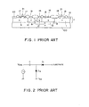
- FIG. 1 A conventional Bi-CMOS integrated circuit including an NPN-type bipolar transistor and a CMOS transistor formed on the same substrate is shown in FIG. 1.
- This Bi-CMOS integrated circuit is formed as follows. An N-type buried layer 6 is formed in a predetermined region on the P-type substrate 100. An N-type layer 7 is then formed by epitaxial growth on the entire surface. Subsequently, an N well 8 serving as the collector region of the NPN type transistor is formed in the layer 7 on the N-type buried layer 6, and an N well 9 for a P-channel MOS transistor region, a P well 10 for isolation which isolates these N wells 9 and 8, and a P well 11 for an N-channel MOS transistor region are formed in respective predetermined regions of the layer 7.
- an N-type layer 12 is formed within the N well 8 so as to reach the buried layer 6.
- an N-type diffused layer 14 serving as the collector electrode is formed within the N-type layer 12, and a P-type diffused layer 15 serving as the base is formed within the N-channel 8 for the collector region.
- an N-type diffused layer 16 serving as the emitter is formed by implantation/diffusion process within the P-type diffused layer 15.
- An NPN transistor is thus formed.
- polysilicon is used to form a gate 21 within the N well 9 for the P-channel MOS transistor.
- a P-type diffused layer 17 serving as a drain/source region is formed. A P-MOS transistor is thus completed.
- CMOS transistor section biases the N well region 9 of the P-channel MOS transistor so that it has a power supply level, and biases the P well region 11 of the N-channel MOS transistor so that it has a ground level.
- an approach is employed to biases the P well region 11 of the N-MOS transistor so that it has a level corresponding to an output from the substrate bias circuit comprised of a capacitor C and rectifier elements Di and D 2 as shown in FIG. 2 in place of the ground level.
- the substrate bias circuit comprised of a capacitor C and rectifier elements Di and D 2 as shown in FIG. 2 in place of the ground level.
- an object of this invention is to provide a Bi-CMOS integrated circuit which can realize a high speed operation of the N-channel MOS transistor.
- a Bi-CMOS integrated circuit comprising: an NPN transistor formed on a substrate surface, a CMOS transistor comprised of a P-channel MOS transistor and an N-channel MOS transistor, formed on said substrate surface, and an N-type region for isolation for electrically isolating a P-type region for isolation between bipolar/CMOS adjoining a N-type region serving as the collector of said NPN transistor and a P-type region of said P-channel MOS transistor.
- the N-type isolation region is formed in a manner to be electrically isolated from the P-type region for the N-channel MOS transistor. Since there is employed a scheme such that potentials are delivered from bias circuits different from each other to the P-type isolation region and the P-type region, respectively, high speed operation can be attained without causing an erroneous operation.
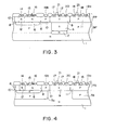
- a first embodiment of a Bi-CMOS integrated circuit according to this invention will now be described with reference to FIG. 3.
- the Bi-CMOS integrated circuit of the first embodiment will be formed as follows.
- an N-type buried layer 2 is formed on an N-type substrate 1.
- a P-type layer 3 is then formed by epitaxial growth on the entire surface.
- An N well 4 is formed in the region of the P-type layer 3 on the buried layer 2 so that it is connected to the buried layer 2.
- an N-type buried layer 6 is formed in the region on the P-type layer 3 where an NPN-type bipolar transistor is formed.
- a P-type layer 7 is formed by epitaxial growth on the entire surface for a second time.
- an N well 9 for the P-MOS transistor is formed in the region of the P-type layer 7 on the N well 4 so that it is connected to the N well 4.
- an N well 8 for the NPN type bipolar transistor is formed in the region of the P-type layer 7 on the buried layer 6 so that it is connected to the buried layer 6.
- an isolation region 10 corresponding to the P-type region or the P well region for separating the P-MOS transistor and the NPN-type bipolar transistor.
- a P well 11 for the N-MOS transistor is formed in the region of the P-type layer 7 adjoining the N well 9 by a process similar to the process for manufacturing the conventional Bi-CMOS integrated circuit.
- an N-type layer 12 is formed within the N well 8 so as to reach the buried layer 6.
- an N-type diffused layer 14 serving as the collector electrode is formed within the N-type layer 12, and a P-type diffused layer 15 serving as the base is formed within the N well 8 for the collector region. Further, an N-type layer 16 serving as the emitter is formed by implantation/diffusion process, etc. within the P-type diffused layer 15. An NPN transistor is thus formed. Subsequently, polysilicon is used to form a gate 21 within the N-well 9 for the P-MOS transistor. Further, a P-type diffused layer 17 serving as the drain/source region is formed. A P-MOS transistor is thus completed. Similarly, polysilicon is used to form a gate 21 within the P well 11.
- an N-type diffused layer 18 serving as the drain/source region is formed to thereby form an N-MOS transistor.
- P-type diffused layers 19a and 19b for bias are formed within the regions of the P well 11 and the P well 10 for isolation, and an N-type diffused layer 20 for bias is formed within the region of the N well 9.
- a Bi-CMOS integrated circuit is thus formed.
- the P well 11 for the N-MOS transistor and the P well 10 for isolation are completely electrically isolated from each other by the N well 9 for the P-MOS transistor, the N well 4, the N-type buried layer 2, and the N-type substrate 1, it is possible to bias individually the P well 10 for isolation and the P well 11 for the N-MOS transistor.
- the P well 10 for separation so that it has a ground level
- biasing the P well 11 for the N-MOS transistor so that it has a corresponding to an output from the substrate bias circuit, e.g., as shown in FIG. 2
- high speed operation can be attained without causing an erroneous operation.
- the N well 9 for the P-MOS transistor is biased so that it has a power supply level.
- the N-type buried layer 2 completely ensures an electrical connection of the N well 4 and the N-type substrate 1. However, if an electrical connection of the N well 4 and the N-type substrate 1 is completely established, the N-type buried layer 2 may be omitted. Furthermore, while the P wells 10 and 11 are formed within the P-type epitaxial layer 7 in the above-described embodiment, it is not necessarily required to form these P wells 10 and 11. In addition, an N-type epitaxial layer 7 may be formed in place of the P-type epitaxial layer 7. At this time, it is not necessarily required to form N wells 8 and 9.
- FIG. 4 A second embodiment of a Bi-CMOS integrated circuit according to this invention is shown in FIG. 4.
- the Bi-CMOS integrated circuit of this embodiment is formed as follows. Initially, P wells 5a and 5b for separation are formed in predetermined regions on an N-type substrate 1, respectively. Further, an N-type buried layer 6 is formed in a region where an NPN-type bipolar transistor is formed within the P well 5a for separation. An N-type epitaxial layer 7 is then formed. Subsequently, a process similar to that of the first embodiment is used to form an NPN-type bipolar transistor and a MOS transistor. Thus, a Bi-CMOS integrated circuit is completed.
- the P wells 5a and 10 for separation and P wells 11 and 5b for the N-channel MOS transistor are electrically isolated from each other by the N well 9 for the P-channel MOS transistor and the N-type substrate 1, it is possible to individually bias the P wells 5a and 10 for separation and the P wells 11 and 5b for the N-channel MOS transistor, respectively.
- high speed operation can be attained without causing an erroneous operation.
- N wells may be formed at the same time in regions except for the regions where these P wells 5a and 5b are formed.
- N wells 8 and 9 are formed within the N-type epitaxial layer 7 in the second embodiment, it is not necessarily required to form N wells 8 and 9.
- a P-type epitaxial layer may be formed in place of the N-type epitaxial layer 7. At this time, it is not necessarily required to form P wells 10 and 11.
- FIG. 5 is a cross sectional view showing respective components of a third embodiment according to this invention, wherein the same or similar reference numerals are attached to portions equivalent or similar to those of the embodiments shown in FIGS. 3 and 4, respectively, and the detailed description will be omitted.
- a Bi-CMOS integrated circuit of FIG. 5 has a structure similar to the structure of FIG. 4, wherein a trench-shaped N-type isolation layer 30 is provided in place of the N well 9 for the P-channel transistor. Trenching is carried out by a well known method. The depth of the trench thus formed is set to a value larger than the thickness of the epitaxial layer 7.
- the P wells 5a and 10 for isolation and the P well 11 for the N-channelf MOS transistor are electrically isolated by the trench 30 and the N-type substrate 1, it is possible to individually apply bias voltages thereto, respectively. Thus, high speed operation can be attained while preventing an erroneous operation.
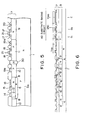
- FIG. 6 shows a fourth embodiment of this invention.
- a substrate bias circuit 40 composed of a plurality of transistors are formed on the surface of the epitaxial layer 7.
- the substrate bias circuit By forming the substrate bias circuit on the chip in this way, the quantity of draw-out wires to the external can be reduced.
Landscapes
- Metal-Oxide And Bipolar Metal-Oxide Semiconductor Integrated Circuits (AREA)
Applications Claiming Priority (2)
| Application Number | Priority Date | Filing Date | Title |
|---|---|---|---|
| JP276896/89 | 1989-10-24 | ||
| JP1276896A JPH03138974A (ja) | 1989-10-24 | 1989-10-24 | Bi―CMOS集積回路 |
Publications (2)
| Publication Number | Publication Date |
|---|---|
| EP0424926A2 true EP0424926A2 (fr) | 1991-05-02 |
| EP0424926A3 EP0424926A3 (en) | 1992-04-15 |
Family
ID=17575904
Family Applications (1)
| Application Number | Title | Priority Date | Filing Date |
|---|---|---|---|
| EP19900120433 Withdrawn EP0424926A3 (en) | 1989-10-24 | 1990-10-24 | Bi-cmos integrated circuit |
Country Status (3)
| Country | Link |
|---|---|
| EP (1) | EP0424926A3 (fr) |
| JP (1) | JPH03138974A (fr) |
| KR (1) | KR910008858A (fr) |
Cited By (6)
| Publication number | Priority date | Publication date | Assignee | Title |
|---|---|---|---|---|
| DE4223272A1 (de) * | 1991-07-17 | 1993-01-21 | Mitsubishi Electric Corp | Halbleitervorrichtung und verfahren zu deren herstellung |
| DE4411869A1 (de) * | 1994-04-06 | 1995-10-12 | Siemens Ag | Integrierte Schaltungsanordnung zum Treiben einer induktiven Last |
| US5517820A (en) * | 1993-03-17 | 1996-05-21 | Hitachi, Ltd. | Exhaust gas purifying apparatus and method for internal combustion engine |
| WO2004032201A3 (fr) * | 2002-09-17 | 2004-06-10 | Infineon Technologies Ag | Procede de fabrication de contacts ohmiques a faible resistance entre substrats et puits dans des circuits integres cmos |
| WO2006055486A3 (fr) * | 2004-11-16 | 2006-07-27 | Transmeta Corp | Systemes et procedes de distribution de tension via des couches epitaxiales |
| US7598573B2 (en) | 2004-11-16 | 2009-10-06 | Robert Paul Masleid | Systems and methods for voltage distribution via multiple epitaxial layers |
Families Citing this family (4)
| Publication number | Priority date | Publication date | Assignee | Title |
|---|---|---|---|---|
| FR2736920B1 (fr) * | 1995-07-21 | 1997-08-22 | Atochem Elf Sa | Compositions thermoplastiques a tenue au feu amelioree |
| JP4784739B2 (ja) * | 2005-10-21 | 2011-10-05 | セイコーエプソン株式会社 | 半導体装置 |
| JP4784738B2 (ja) * | 2005-10-21 | 2011-10-05 | セイコーエプソン株式会社 | 半導体装置 |
| KR20230116572A (ko) * | 2022-01-28 | 2023-08-04 | 롯데케미칼 주식회사 | 열가소성 수지 조성물 및 이를 이용한 성형품 |
Family Cites Families (5)
| Publication number | Priority date | Publication date | Assignee | Title |
|---|---|---|---|---|
| JPS4842685A (fr) * | 1971-09-30 | 1973-06-21 | ||
| US4566914A (en) * | 1983-05-13 | 1986-01-28 | Micro Power Systems, Inc. | Method of forming localized epitaxy and devices formed therein |
| JPS61115349A (ja) * | 1984-11-09 | 1986-06-02 | Mitsubishi Electric Corp | 半導体集積回路装置 |
| JPS63161658A (ja) * | 1986-12-25 | 1988-07-05 | Nec Corp | 半導体集積回路装置 |
| US4825275A (en) * | 1987-05-28 | 1989-04-25 | Texas Instruments Incorporated | Integrated bipolar-CMOS circuit isolation for providing different backgate and substrate bias |
-
1989
- 1989-10-24 JP JP1276896A patent/JPH03138974A/ja active Pending
-
1990
- 1990-10-23 KR KR1019900016940A patent/KR910008858A/ko not_active Abandoned
- 1990-10-24 EP EP19900120433 patent/EP0424926A3/en not_active Withdrawn
Cited By (9)
| Publication number | Priority date | Publication date | Assignee | Title |
|---|---|---|---|---|
| DE4223272A1 (de) * | 1991-07-17 | 1993-01-21 | Mitsubishi Electric Corp | Halbleitervorrichtung und verfahren zu deren herstellung |
| US5517820A (en) * | 1993-03-17 | 1996-05-21 | Hitachi, Ltd. | Exhaust gas purifying apparatus and method for internal combustion engine |
| DE4411869A1 (de) * | 1994-04-06 | 1995-10-12 | Siemens Ag | Integrierte Schaltungsanordnung zum Treiben einer induktiven Last |
| US5719431A (en) * | 1994-04-06 | 1998-02-17 | Siemens Aktiengesellschaft | Integrated driver circuit configuration for an inductive load element |
| WO2004032201A3 (fr) * | 2002-09-17 | 2004-06-10 | Infineon Technologies Ag | Procede de fabrication de contacts ohmiques a faible resistance entre substrats et puits dans des circuits integres cmos |
| WO2006055486A3 (fr) * | 2004-11-16 | 2006-07-27 | Transmeta Corp | Systemes et procedes de distribution de tension via des couches epitaxiales |
| US7598573B2 (en) | 2004-11-16 | 2009-10-06 | Robert Paul Masleid | Systems and methods for voltage distribution via multiple epitaxial layers |
| US7667288B2 (en) | 2004-11-16 | 2010-02-23 | Masleid Robert P | Systems and methods for voltage distribution via epitaxial layers |
| TWI418029B (zh) * | 2004-11-16 | 2013-12-01 | 智慧投資基金有限責任公司 | 藉由磊晶層用於電壓分佈的系統與方法 |
Also Published As
| Publication number | Publication date |
|---|---|
| JPH03138974A (ja) | 1991-06-13 |
| EP0424926A3 (en) | 1992-04-15 |
| KR910008858A (ko) | 1991-05-31 |
Similar Documents
| Publication | Publication Date | Title |
|---|---|---|
| US4825275A (en) | Integrated bipolar-CMOS circuit isolation for providing different backgate and substrate bias | |
| US5376816A (en) | Bi-cmos integrated circuit device having buried region use in common for bipolar and mos transistors | |
| US5087579A (en) | Method for fabricating an integrated bipolar-CMOS circuit isolation for providing different backgate and substrate bias | |
| EP0009782B1 (fr) | Dispositif semi-conducteur du type CMOS | |
| US6054344A (en) | OTP (open trigger path) latchup scheme using buried-diode for sub-quarter micron transistors | |
| US4912054A (en) | Integrated bipolar-CMOS circuit isolation process for providing different backgate and substrate bias | |
| US5060044A (en) | Integrated bipolar-CMOS circuit isolation for providing different backgate and substrate bias | |
| JP3120447B2 (ja) | 集積回路の動的分離用回路 | |
| JPS6250985B2 (fr) | ||
| US6033947A (en) | Driving circuit for electronic semiconductor devices including at least a power transistor | |
| EP0424926A2 (fr) | Circuit intégré du type BiCMOS | |
| US5583363A (en) | Inverter gate circuit of a bi-CMOS structure having common layers between fets and bipolar transistors | |
| US5859562A (en) | Programming circuit for antifuses using bipolar and SCR devices | |
| EP0703620B1 (fr) | Circuit pour prévenir l'amorçage de composants parasites dans des circuits intégrés comprenant un étage de puissance et un circuit de commande basse tension | |
| US5168341A (en) | Bipolar-cmos integrated circuit having a structure suitable for high integration | |
| JPS6197858A (ja) | 半導体装置 | |
| US5371023A (en) | Gate circuit, semiconductor integrated circuit device and method of fabrication thereof, semiconductor memory and microprocessor | |
| US5773864A (en) | CMOS interface circuit formed in silicon-on-insulator substrate | |
| US5172209A (en) | Integral Bi-CMOS logic circuit | |
| JPS63252464A (ja) | 半導体装置 | |
| JPH11251447A (ja) | 半導体装置及びその製造方法 | |
| JP4025474B2 (ja) | 半導体増幅回路 | |
| JP2523506B2 (ja) | 半導体装置 | |
| JP2730450B2 (ja) | 半導体装置 | |
| US6275095B1 (en) | Semiconductor amplifier circuit |
Legal Events
| Date | Code | Title | Description |
|---|---|---|---|
| PUAI | Public reference made under article 153(3) epc to a published international application that has entered the european phase |
Free format text: ORIGINAL CODE: 0009012 |
|
| 17P | Request for examination filed |
Effective date: 19901024 |
|
| AK | Designated contracting states |
Kind code of ref document: A2 Designated state(s): DE FR GB |
|
| PUAL | Search report despatched |
Free format text: ORIGINAL CODE: 0009013 |
|
| AK | Designated contracting states |
Kind code of ref document: A3 Designated state(s): DE FR GB |
|
| STAA | Information on the status of an ep patent application or granted ep patent |
Free format text: STATUS: THE APPLICATION HAS BEEN WITHDRAWN |
|
| 18W | Application withdrawn |
Withdrawal date: 19931013 |