EP0425084A1 - Verfahren zur Abscheidung von einem Film mittels eines Alkylaluminiumhydrids - Google Patents
Verfahren zur Abscheidung von einem Film mittels eines Alkylaluminiumhydrids Download PDFInfo
- Publication number
- EP0425084A1 EP0425084A1 EP90309800A EP90309800A EP0425084A1 EP 0425084 A1 EP0425084 A1 EP 0425084A1 EP 90309800 A EP90309800 A EP 90309800A EP 90309800 A EP90309800 A EP 90309800A EP 0425084 A1 EP0425084 A1 EP 0425084A1
- Authority
- EP
- European Patent Office
- Prior art keywords
- film
- substrate
- process according
- electron
- deposited
- Prior art date
- Legal status (The legal status is an assumption and is not a legal conclusion. Google has not performed a legal analysis and makes no representation as to the accuracy of the status listed.)
- Granted
Links
Images





Classifications
-
- H—ELECTRICITY
- H10—SEMICONDUCTOR DEVICES; ELECTRIC SOLID-STATE DEVICES NOT OTHERWISE PROVIDED FOR
- H10P—GENERIC PROCESSES OR APPARATUS FOR THE MANUFACTURE OR TREATMENT OF DEVICES COVERED BY CLASS H10
- H10P14/00—Formation of materials, e.g. in the shape of layers or pillars
- H10P14/40—Formation of materials, e.g. in the shape of layers or pillars of conductive or resistive materials
- H10P14/42—Formation of materials, e.g. in the shape of layers or pillars of conductive or resistive materials using a gas or vapour
- H10P14/43—Chemical deposition, e.g. chemical vapour deposition [CVD]
- H10P14/432—Chemical deposition, e.g. chemical vapour deposition [CVD] using selective deposition
-
- C—CHEMISTRY; METALLURGY
- C23—COATING METALLIC MATERIAL; COATING MATERIAL WITH METALLIC MATERIAL; CHEMICAL SURFACE TREATMENT; DIFFUSION TREATMENT OF METALLIC MATERIAL; COATING BY VACUUM EVAPORATION, BY SPUTTERING, BY ION IMPLANTATION OR BY CHEMICAL VAPOUR DEPOSITION, IN GENERAL; INHIBITING CORROSION OF METALLIC MATERIAL OR INCRUSTATION IN GENERAL
- C23C—COATING METALLIC MATERIAL; COATING MATERIAL WITH METALLIC MATERIAL; SURFACE TREATMENT OF METALLIC MATERIAL BY DIFFUSION INTO THE SURFACE, BY CHEMICAL CONVERSION OR SUBSTITUTION; COATING BY VACUUM EVAPORATION, BY SPUTTERING, BY ION IMPLANTATION OR BY CHEMICAL VAPOUR DEPOSITION, IN GENERAL
- C23C16/00—Chemical coating by decomposition of gaseous compounds, without leaving reaction products of surface material in the coating, i.e. chemical vapour deposition [CVD] processes
- C23C16/06—Chemical coating by decomposition of gaseous compounds, without leaving reaction products of surface material in the coating, i.e. chemical vapour deposition [CVD] processes characterised by the deposition of metallic material
- C23C16/18—Chemical coating by decomposition of gaseous compounds, without leaving reaction products of surface material in the coating, i.e. chemical vapour deposition [CVD] processes characterised by the deposition of metallic material from metallo-organic compounds
- C23C16/20—Deposition of aluminium only
-
- Y—GENERAL TAGGING OF NEW TECHNOLOGICAL DEVELOPMENTS; GENERAL TAGGING OF CROSS-SECTIONAL TECHNOLOGIES SPANNING OVER SEVERAL SECTIONS OF THE IPC; TECHNICAL SUBJECTS COVERED BY FORMER USPC CROSS-REFERENCE ART COLLECTIONS [XRACs] AND DIGESTS
- Y10—TECHNICAL SUBJECTS COVERED BY FORMER USPC
- Y10S—TECHNICAL SUBJECTS COVERED BY FORMER USPC CROSS-REFERENCE ART COLLECTIONS [XRACs] AND DIGESTS
- Y10S438/00—Semiconductor device manufacturing: process
- Y10S438/937—Hillock prevention
Definitions
- This invention relates to a process for forming a deposited film, particularly a process for forming an Al deposited film which can be preferably applied to electrodes or wiring of a semiconductor integrated circuit device, etc.
- Al aluminum
- Al has many advantages such that it is inexpensive and high in electroconductivity, that it can be also internally chemically protected because a dense oxidized film can be formed on the surface, and that it has good adhesion to Si, etc.
- the aspect ratio (via-hole depth/via-hole diameter) of via-hole in which a metal composed mainly of Al such as Al, Al-Si, etc. is to be deposited is 1.0 or more, and the via-hole diameter itself also becomes 1 ⁇ m or less. Therefore, even for a via-hole with large aspect ratio, the technique which can deposit a metal is required.
- Al is required to be deposited so as to embed only the via-hole of the device.
- a method of depositing Al only on Si or metal surface and not depositing it on an insulating film such as SiO2, etc. is required.
- the sputtering method is a physical deposition method based on flying of the particles sputtered from the target in vacuum, the film thickness at the stepped portion or the insulating film side wall becomes extremely thin, leading even to wire breaking in an extreme case. And, nonuniformity of the film thickness and wire breaking will markedly lower reliability of LSI.
- the bias sputtering method in which a bias is applied on a substrate and deposition is performed so as to embed Al or an Al alloy only in the via-hole by utilizing the sputter etching action and the deposition action on the substrate surface.
- the bias voltage of some 100 V or higher is applied on the substrate, deleterious influence on the device occurs because of charged particle damaging such as change in threshold of MOS FET, etc.
- the deposition speed cannot be essentially improved.
- CVD Chemical Vapor Deposition
- plasma CVD or optical CVD decomposition of the starting gas occurs in gas phase, and the active species formed there further reacts on the substrate to give rise to film formation.
- plasma CVD or optical CVD due to the reaction in gas phase, surface coverage on unevenness on the substrate surface is good.
- carbon atoms contained in the starting gas molecule are incorporated into the film.
- plasma CVD the problem remained that there was damage by charged particles (so called plasma damage) as in the case of the sputtering method.
- the thermal CVD method in which the film grows through the surface reaction primarily on the substrate surface, is good in surface coverage on unevenness such as stepped portion of the surface, etc. Also, it can be expected that deposition within via-hole will readily occur. Further, wire breaking at the stepped portion can be avoided.
- the thermal CVD method has been variously studied.
- As the formation method of Al film according to general thermal CVD there is used a method of transporting an organic aluminum dispersed in carrier gas to a heated substrate and pyrolyzing the gas molecules on the substrate to form a film.
- a method of transporting an organic aluminum dispersed in carrier gas to a heated substrate and pyrolyzing the gas molecules on the substrate to form a film.
- TIBA triisobutyl aluminum
- film formation is effected at a film formation temperature of 260 o C and a reaction tube pressure of 0.5 torr to form a film of 3.4 ⁇ ohm ⁇ cm.
- Japanese Laid-open Patent Application No. 63-33569 describes a method of forming a film by using no TiCl4, but using in place thereof organic aluminum such as TIBA and heating it in the vicinity of the substrate. According to this method, Al can be deposited selectively only on the metal or semiconductor surface from which the naturally oxidized film has been removed.
- the present invention has been accomplished in view of the technical tasks as described above, and an object of the present invention is to provide a process for forming a deposited film which can form an Al film (hereinafter referring comprehensively to pure Al and a metal composed mainly of Al) of good quality as the electroconductive material at a desired position with good controllability.
- Another object of the present invention is to provide a process for forming a deposited film which can obtain an Al film which has extremely broad general purpose utility and yet is of good quality, without requiring particularly no complicated and expensive deposited film forming device.
- Still another object of the present invention is to provide a process for forming a deposited film which can form an Al film excellent in surface characteristic, electrical characteristics, purity, etc. according to the CVD method utilizing alkyl aluminum hydride and hydrogen.
- Still another object of the present invenion is to provide a process for forming a deposited film of an Al film which is extremely broad in general purpose utility and excellent in selectivity, without requiring particularly a complicated and expensive deposited film forming device.
- Still another object of the present invention is to provide a process for forming a deposited film which can form an Al film under good selectivity according to the CVD method utilizing alkyl aluminum hydride and hydrogen.
- Another preferred embodiment of the present invention is a process for forming a deposited film comprising the steps of:
- the decomposition reaction of an organic metal and hence the thin film deposition reaction will vary greatly depending on the kind of the metal atom, the kind of the alkyl bonded to the metal atom, the means of causing the decomposition reaction to occur, the atmospheric gas, etc.
- trimethyl gallium: in thermal decomposition undergoes radical cleavage wherein Ga-CH3 bond is cleaved
- triethyl gallium: in thermal decomposition is decomposed through ⁇ -elimination into: and C2H4.
- triethyl aluminum attached with the same ethyl group: in thermal decomposition undergoes radical decomposition in which Al-C2H5 is cleaved.
- tri-iso-butyl aluminum having ic4H9 bonded therein: is subject to ⁇ -elimination.
- Trimethyl aluminum (TMA) comprising CH3 groups and Al has a dimer structure at room temperature: and thermal decomposition is radical decomposition in which Al-CH3 group is cleaved, and at a temperature of 150 o C or lower, it reacts with atmospheric H2 to form CH4, and forms finally Al.
- C2H6 will be formed by the bridging CH3 between two Al's.
- the excitation decomposition means for deposition of a metal atom from an organic metal on a desired substrate
- the decomposition reaction must be strictly controlled.
- Al is to be deposited from triisobutyl aluminum: in the low pressure CVD method comprising mainly thermal reaction, unevenness of um order is formed on the surface, whereby the surface morphology is inferior.
- hillock generation by heat treatment, Si surface roughening through Si diffusion at the interface between Al and Si occur, and also migration resistance is inferior, whereby it can be utilized for ultra-LSI process with difficulty.
- the device is complicated, and the method is of the sheet treatment type in which deposition can be effected only on one wafer by one deposition process. Besides, since the deposition speed is 500 A/min. at the highest, the throughput necessary for bulk production cannot be realized.
- Dimethyl aluminum hydride (DMAH) as the alkyl aluminum hydride to be utilized in the present invention is a substance known as alkyl metal, but it could not be estimated at all what Al thin film could be deposited depending on what reaction mode, unless deposited films are formed under all the conditions.
- DMAH Dimethyl aluminum hydride
- the surface morphology is inferior, and the resistivity value was greater than the bulk value (2.7 ⁇ ohm ⁇ cm) as several ⁇ ohm to 10 ⁇ ohm ⁇ cm, thus being inferior in film quality.
- the CVD method for depositing selectively an Al film of good quality as the electroconductive deposition film on a substrate, the CVD method is used.
- DMAH dimethyl aluminum hydride
- MMAH2 monomethyl aluminum hydride
- a material having an electron donative surface may be employed.
- the electron donative material is described in detail below.
- the electron donative material refers to one having free electrons existing or free electrons intentionally formed in the substrate, for example, a material having a surface on which the chemical reaction is promoted through give-and-take of electrons with the starting gas molecules attached on the substrate surface.
- a material having a surface on which the chemical reaction is promoted through give-and-take of electrons with the starting gas molecules attached on the substrate surface For example, generally metals and semiconductors correspond to such material. Those having very thin oxidized film on the metal or semiconductor surface are also included. For, with such thin film, the chemical reaction can occur between the substrate and the attached starting molecules.
- semiconductors such as monocrystalline silicon, polycrystalline silicon, amorphous silicon, etc., binary system or ternary system or quaternary system III-V compound semiconductors comprising combinations of Ga, In, Al as the group III element and P, As, N as the group V element, or II-IV compound semiconducters, or metals themselves such as tungsten, molybdenum, tantalum, aluminum, titanium, copper, etc., or silicides of the above metals such as tungsten silicide, molybdenum silicide, tantalum silicide, aluminum silicide, titanium silicide, etc., further metals containing either one of the constituent of the above metals such as aluminum silicon, aluminum titanium, aluminum copper, aluminum tantalum, aluminum silicon copper, aluminum silicon titanium, aluminum palladium, titanium nitride, etc.
- semiconductors such as monocrystalline silicon, polycrystalline silicon, amorphous silicon, etc., binary system or ternary system or quaternary system III-V compound semiconductors comprising combinations of Ga,
- the thermal reaction in the reaction system between DMAH and H2 may be basically considered as follows: DMAH assumes a dimer structure at room temperature. Also, with MMAH2, a high quality Al film could be formed by thermal reaction as shown below in Examples.
- MMAH2 has low vapor pressure as 0.01 to 0.1 Torr at room temperature, a large amount of the starting material can be transported with difficulty, and the upper limit value of the deposition speed is several hundred ⁇ /min. in the present embodiment, and preferably, it is most desirable to use DMAH of which vapor pressure is 1 Torr at room temperature.
- the CVD method is used for selective deposition of a good Al film as the electroconductive deposition film on the substrate.
- DMAH dimethyl aluminum hydride
- MMAH2 monomethyl aluminum hydride
- the substrate applicable in the present invention has a first substrate surface material for formation of the surface on which Al is deposited, and a second substrate surface material on which no Al is deposited. And, as the first substrate surface material, a material having the electron donative surface is used.
- the material for forming the surface on which Al is not deposited selectively namely the material for forming the electron non-donative surface
- conventional insulating materials oxidized silicon formed by thermal oxidation, CVD, etc., glass or oxidized film such as BSG, PSG, BPSG, etc., thermally nitrided film, silicon nitrided film by plasma CVD, low pressure CVD, ECR-CVD method, etc.
- Fig. 1 is a schematic view showing a preferable deposition film forming device for applying the present invention.
- 1 is a substrate for forming an Al film.
- the substrate 1 is mounted on a substrate holder 3 provided internally of the reaction tube 2 for forming a space for formation of a deposited film which is substantially closed to Fig. 1.
- quartz is preferable, but it may be also made of a metal. In this case, it is preferable to cool the reaction tube.
- the substrate holder 3 is made of a metal, and is provided with a heater 4 so that the substrate mounted thereon can be heated. And, the constitution is made so that the substrate temperature can be controlled by controlling the heat generation temperature of the heater 4.
- the feeding system of gases is constituted as described below.
- 5 is a gas mixer, in which the starting gas and the reaction gas are mixed, and the mixture is fed into the reaciton tube 2.
- 6 is a starting gas gasifier provided for gasification of an organic metal as the starting gas.
- the organic metal to be used in the present invention is liquid at room temperature, and is formed into saturated vapor by passing a carrier gas through the liquid of the organic metal within the gasifier 6, which is in turn introduced into the mixer 5.
- the evacuation is constituted as described below.
- a gate valve which is opened when performing evacuation of a large volume such as during evacuation internally of the reaction tube 2 before formation of the deposited film.
- 8 is a slow leak valve, which is used when performing evacuation of a small volume such as in controlling the pressure internally of the reaction tube 2 during formation of the deposited film.
- 9 is an evacuation unit, which is constituted of a pump for evacuation such as turbo molecular pump, etc.
- the conveying system of the substrate 1 is constituted as described below.
- 10 is a substrate conveying chamber which can house the substrate before and after formation of the deposited film, which is evacuated by opening the valve 11.
- 12 is an evacuation unit for evacuating the conveying chamber, which is constituted of a pump for evacuation such as turbo molecular pump, etc.
- the valve 13 is opened only when the substrate 1 is transferred between the reaction chamber and the conveying space.
- the liquid DMAH maintained at room temperature is bubbled with H2 or Ar (or other inert gas) as the carrier gas to form gaseous DMAH, which is transported to the mixer 5.
- H2 gas as the reaction gas is transported through another route into the mixer 5.
- the gases are controlled in flow rates so that the respective partial pressures may become desired values.
- the starting gas may be of course MMAH2, but DMAH with a vapor pressure enough to become 1 Torr at room temperature is the most preferred. Also, DMAH and MMAH2 may be used in a mixture.
- the deposited film formed at a substrate temperature of 160 o C to 450 o C by use of such starting gas and reaction gas, with a thickness of for example 400 ⁇ has a resistivity at room temperature of 2.7 - 3.0 ⁇ ohm ⁇ cm which is substantially equal to Al bulk resistivity, and is a continuous and flat film.
- the pressure during film formation can be chosen within the range from 10 ⁇ 3 Torr to 760 Torr.
- the film thickness may be 1 ⁇ m
- its resistivity is ca. 2.7 - 3.0 ⁇ ohm ⁇ cm, and a sufficiently dense film can be formed also with a relatively thicker film.
- the reflectance in the visible light wavelength region is approximately 80 %, whereby a thin film excellent in surface flatness can be deposited.
- the substrate temperature is desirably the decomposition temperature of the starting gas containing Al or higher, and 450 o C or lower as described above, but specifically the substrate temperature of 200 to 450 o C is more desirable, and when deposition is carried out under this condition, by making the DMAH partial pressure 10 ⁇ 4 to 10 ⁇ 3 Torr, the deposition speed becomes very great as 100 ⁇ /min. to 800 ⁇ /min., whereby sufficient great deposition speed corresponding to the cost as the Al deposition technique for ultra-LSI can be obtained.
- a more preferable substrate temperature condition is 270 o C to 350 o C, and the Al film deposited under this condition is also strongly orientatable and, even when subjected to the heat treatment at 450 o C for 1 hour, the Al film on the Si monocrystalline or Si polycrystalline substrate becomes a good Al film without generation of hillock, spike as seen in the film forming method of the prior art. Also, such Al film is excellent in electromigration resistance.
- Al can be deposited on only one sheet of substrate in deposition for one time. Although a deposition speed of ca. 800 ⁇ /min. can be obtained, it is still insufficient for performing deposition of a large number of sheets within a short time.
- the deposition film forming device for improving this point there is the low pressure CVD device which can deposit Al by simultaneous mounting of a large number of sheets of wafer. Since the Al film formation according to the present embodiment utilizes the surface reaction on the electron donative substrate surface, in the hot wall type low pressure CVD method wherein only the substrate is heated, Al can be deposited on the substrate by use of DMAH and H2.
- the reaction tube pressure may be 0.05 to 760 Torr, desirably 0.1 to 0.8 Torr, the substrate temperature 160 o C to 450 o C, desirably 200 o C to 400 o C, the DMAH partial pressure 1 x 10 ⁇ 5-fold to 1.3 x 10 ⁇ 3-fold of the pressure in the reaction tube, and under such conditions, Al can be well deposited on the electron donative substrate.
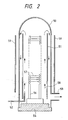
- Fig. 2 is a schematic illustration showing a deposited film forming device to which such present invention is applicable.
- 57 is a substrate for formation of Al film.
- 50 is an outside reaction tube made of quartz for forming a space for formation of deposited film substantially closed to the surrounding, 51 an innerside reaction tube made of quartz located for separating the flow of gas within the outside reaction tube 50, 54 a flange made of a metal for opening and closing of the opening of the outside reaction tube 50, and the substrate 57 is located within the substrate holding member 56 provided internally of the innerside reaction tube 51.
- the substrate holding member 56 should be preferably made of quartz.
- the substrate temperature can be controlled by the heater portion 59.
- the pressure internally of the reaction tube 50 is constituted so as to be controllable by the evacuation system connected through the gas evacuation outlet 53.
- the gas feeding system is constituted to have a first gas system, a second gas system and a mixer (none are shown) similarly as the device shown by the symbols 5 and 6 in Fig. 1, and the starting gas and the reaction gas are introduced into the reaction tube 50 through the starting gas inlet 52. These gases react on the surface of the substrate 57 during passage internally of the innerside reaction tube 51 as shown by the arrowhead 58 in Fig. 2 to deposit Al on the substrate surface. The gases after the reaction pass through the gap formed between the innerside reaction tube 51 and the outside reaction tube 50, and evacuated through the gas evacuation outlet 53.
- the flange 54 made of a metal is permitted to fall by an elevator (not shown) together with the substrate holding member 56 and the substrate 57 to be moved to a predetermined position where the substrate is mounted and detached.
- Al films of good quality can be formed in all the wafers within the device.
- the film obtained according to the Al film formation process based on the embodiment of the present invention is dense with little content of impurity such as carbon, etc. and resistivity which is similar to bulk, and also has high surface smoothness, and therefore remarkable effects as described below can be obtained.
- Hillock is occurrence of concavities on the Al surface due to partial migration of Al when inner stress during film formation is released in the heat treatment step. Also, similar phenomenon occurs by local migration by current passage.
- the Al film formed by the present invention has little inner stress and is under the state of monocrystal or approximate to that. For this reason, in the heat treatment at 450 o C for one hour, as contrasted to formation of 104 - 106/cm2 of hillocks in the Al film of the prior art, the hillock number could be greatly improved as 0 to 10/cm2.
- the resist film thickness and the interlayer insulating film can be made thin to be advantageous for making it finer and more flat.
- Electro-migration is the phenomenon that the wiring atoms move by passage of a current of high density. By this phenomenon, voids are generated and grown along the grain boundary, whereby as accompanied with reduction of the cross-sectional area, the wiring generates heat to be broken.
- Migration resistance is generally evaluated by average wiring life.
- the wiring formed by the sputtering method or the CVD method of the prior art has obtained an average wiring life of 1 x 10² to 103 hours (in the case of a wiring cross-sectional area of 1 ⁇ m2) under the current passage test conditions of 250 o C, 1 x 10⁶ A/cm2.
- the Al film obtained by the Al film formation method based on the embodiment of the present invention could obtain an average wiring life of 103 to 104 hours with a wiring having a cross-sectional area of 1 ⁇ m2.
- a wiring layer thickness of 0.3 ⁇ m can sufficiently stand practical application. That is, since the wiring layer thickness can be made thinner, unevenness on the semiconductor surface after arrangement of wiring can be suppressed minimum, and also high reliability in passing ordinary current can be obtained. Also, this is possible by a very simple process.
- the surface morphology of Al film to be formed is markedly improved to cancell all the drawbacks described above.
- the contact resistivity can attain 1 x 10 ⁇ 6 ohm ⁇ cm2 at an area of 0.6 ⁇ m x 0.6 ⁇ m when the Si portion has an impurity of 1020 cm ⁇ 3.
- the yield can be improved, and reduction of cost can be promoted to great extent as compared with Al wiring of the prior art.
- Figs. 3A - 3E show how the Al film according to the present invention is selectively grown.
- Fig. 3A is an illustration showing schematically the cross-section of the substrate before formation of the Al deposited film according to the present invention.
- 90 is the substrate comprising an electron donative material, and 91 a thin film comprising an electron non-donative material.
- the pressure within the reaction tube 2 should be desirably 10 ⁇ 3 to 760 Torr, and the DMAH partial pressure preferably 1.5 x 10 ⁇ 5 to 1.3 x 10 ⁇ 3-fold of the pressure within the above reaction tube.
- the Al film grows to the level of the uppermost portion of the thin film 91 as shown in Fig. 3D. Further, when grown under the same conditions, as shown in Fig. 3E, the Al film can grow to 5000 ⁇ substantially without growth in the lateral direction. This is the most characteristic point of the deposited film obtained by the present invention, and it will be understood how a film of good quality can be formed under good selectivity.
- the deposited film thus formed has a resistivity of, for example, with a film thickness of 400 ⁇ , 2.7 - 3.0 ⁇ ohm ⁇ cm at room temperature which is substantially equal to the bulk resistivity of Al, and becomes continuous and flat film. Also, even with a film thickness of 1 ⁇ m, its resistance at room temperature is approximately 2.7 - 3.0 ⁇ ohm ⁇ cm and a sufficiently dense film is formed with a relatively thicker film. The reflectance in the visible wavelength region is approximately 80 %, and a thin film with excellent surface flatness can be deposited.
- the substrate temperature in performing such selective deposition should be desirably the decomposition temperature of the starting gas containing Al or higher and 450 o C or lower as mentioned above, but specifically a substrate temperature of 200 to 450 o C is desirable, and when deposition is performed under such condition, the deposition speed is sufficiently great as 100 ⁇ /min. to 800 ⁇ /min. when DMAH partial pressure is 10 ⁇ 4 to 10 ⁇ 3 Torr. Thus a sufficiently great deposition speed can be obtained as the Al deposition technique for ultra-LSI.
- a more preferable substrate temperature condition is 270 o C to 350 o C, and the Al film deposited under this condition is also strongly orientatable and, even when subjected to the heat treatment at 450 o C for 1 hour, the Al film on the Si monocrystalline or Si polycrystalline substrate becomes a good Al film without generation of hillock, spike. Also, such Al film is excellent in electro-migration resistance.
- Al can be deposited on only one sheet of substrate in deposition for one time. Although a deposition speed of ca. 800 ⁇ /min. can be obtained, it is still insufficient for performing deposition of a large number of sheets within a short time.
- the deposition film forming device for improving this point there is the low pressure CVD device which can deposit Al by simultaneous mounting of a large number of sheets of wafer. Since the Al film formation according to the present embodiment utilizes the surface reaction of the electron donative substrate surface, in the hot wall type low pressure CVD method wherein only the substrate is heated, Al can be deposited on the substrate by use of DMAH and H2.
- the reaction tube pressure may be 0.05 to 760 Torr, desirably 0.1 to 0.8 Torr, the substrate temperature 160 o C to 450 o C, desirably 200 o C to 400 o C, the DMAH partial pressure 1 x 10 ⁇ 5-fold to 1.3 x 10 ⁇ 3-fold of the pressure in the reaction tube, and under such conditions, Al can be selectively deposited on only the electron donative substrate.
- the deposited film forming device to which such present invention is applicable is the same as in Fig. 2 as described above, and therefore its detailed description is omitted here.
- Al films of good quality can be formed selectively and simultaneously in all the wafers within the device.
- the film obtained according to the Al film selective formation process based on the embodiment of the present invention is dense with very little content of impurity such as carbon, etc. and resistivity which is similar to bulk, and also has high surface smoothness, and therefore remarkable effects as described below can be obtained.
- the Al film formed according to the present invention has little internal stress and is under the state of monocrystal or approximate to that. For this reason, in the heat treatment at 450 o C for one hour, as contrasted to formation of 104 - 106/cm2 of hillrocks in the Al film of the prior art, the hillrock number could be greatly improved as 0 to 10/cm2.
- the wiring formed by the method of the prior art has obtained an average wiring life of 1 x 10² to 103 hours (in the case of a wiring cross-sectional area of 1 ⁇ m2) under the current passage test conditions of 250 o C, 1 x 10⁶ ⁇ /cm2.
- the Al film obtained by the Al film selective formation method based on the embodiment of the present invention could obtain an average wiring life of 103 to 104 hours with a wiring having a cross-sectional area of 1 ⁇ m2.
- the Al selectively formed according to the present invention can suppress generation of alloy pit at the contact portion with the substrate crystal even by the heat treatment during wiring step, and also a wiring with good contact characteristic can be obtained. That is, even when the junction is made shallow to the extent of 0.1 ⁇ m, the junction will not be destroyed with only the Al material.
- the surface morphology of the Al film to be formed can be improved epoch-makingly, whereby all of the problems of the prior art can be improved.
- the contact resistivity can attain 1 x 10 ⁇ 6 ohm ⁇ cm2 in the case where the Si portion has an impurity of 1020cm3 in a hole of 0.6 ⁇ m x 0.6 ⁇ m.
- the wiring material can be completely embedded only in the minute opening, and also good contact with the substrate can be obtained. Therefore, the present invention can contribute greatly to improvement of resistance within hole and contact resistance which have been the greatest problems in the fine process of 1 ⁇ m or less.
- the yield can be improved, and reduction of cost can be promoted to great extent as compared with Al wiring of the prior art.
- the procedure for Al film formation is as follows.
- the reaction tube 2 is internally evacuated to ca. 1 x 10 ⁇ 8 Torr by the evacuation unit 9.
- Al film can be also formed if the vacuum degree within the reaction tube 2 may be higher than 1 x 10 ⁇ 8 Torr.
- the conveying chamber 10 After washing of Si wafer, the conveying chamber 10 is released to atmospheric pressure and Si wafer is mounted in the conveying chamber.
- the conveying chamber is evacuated to ca. 1 x 10 ⁇ 6 Torr, and then the gate valve 13 is opened and the wafer is mounted on the wafer holder 3.
- the gate valve 13 is closed, and the reaction chamber 2 is evacuated to a vacuum degree of ca. 1 x 10 ⁇ 8 Torr.
- DMAH is fed through the first gas line.
- the second gas line is used for H2.
- the pressure within the reaction tube 2 is made a predetermined value by controlling the opening of the slow leak valve 8.
- a typical pressure in this Example is made approximately 1.5 Torr.
- the wafer is heated by current passage through the heater 4.
- DMAH is introduced into the reaction tube through the DMAH line.
- the whole pressure is ca. 1.5 Torr, and the DMAH partial pressure is made ca. 1.5 x 10 ⁇ 4 Torr.
- DMAH is introduced into the reaction tube 2
- Al is deposited.
- feeding of DMAH is stopped.
- heating of the heater 4 is stopped to cool the wafer. Feeding of H2 gas is stopped, and after evacuation internally of the reaction tube, the wafer is transferred to the conveying chamber, and only the conveying chamber is made atmospheric pressure before taking out the wafer.
- the outline of Al film formation is as described above.
- Sheets of samples of monocrystalline Si substrates (N type, 1 - 2 ohm ⁇ cm) were prepared, the substrate temperatures were set at 13 levels, and Al films were deposited at the respective temperatures each for 10 sheets according to the procedure as described above under the following conditions: whole pressure: 1.5 Torr DMAH partial pressure: 1.5 x 10 ⁇ 4 Torr.
- Al films of very good quality were obtained at a temperature range of 160 o C to 450 o C, more preferably 200 o C to 400 o C, optimally 270 o C to 350 o C.
- the procedure of Al film formation is as follows.
- the evacuation unit 9 the reaction tube 2 is evacuated internally to ca. 1 x 10 ⁇ 8 Torr.
- Al film can be formed even if the vacuum degree in the reaction tube 2 may be higher than 1 x 10 ⁇ 8 Torr.
- the conveying chamber 10 After washing of the Si wafer, the conveying chamber 10 is released to atmospheric pressure and the Si wafer is mounted in the conveying chamber.
- the conveying chamber is evacuated to ca. 1 x 10 ⁇ 6 Torr, then the gate valve 13 is opened and the wafer is mounted on the wafer holder 3.
- the gate valve 13 is closed, and the reaction chamber 2 is evacuated to a vacuum degree of ca. 1 x 10 ⁇ 8 Torr.
- the first gas line is used for DMAH.
- Ar is employed as the carrier gas for the DMAH line.
- the second gas line is used for H2.
- the pressure within the reaction tube 2 is made a predetermined value by controlling the opening of the slow leak valve 8.
- a typical pressure in this Example is made approximately 1.5 Torr.
- the wafer is heated by current passage through the heater 4.
- DMAH is introduced into the reaction tube through the DMAH line.
- the whole pressure is ca. 1.5 Torr, and the DMAH partial pressure is made ca. 1.5 x 10 ⁇ 4 Torr.
- DMAH is introduced into the reaction tube 2
- Al is deposited.
- feeding of DMAH is stopped.
- heating of the heater 4 is stopped to cool the wafer. Feeding of H2 gas is stopped, and after evacuation internally of the reaction tube, the wafer is transferred to the conveying chamber, and only the conveying chamber is made atmospheric pressure before taking out the wafer.
- the outline of Al film formation is as described above.
- This Example 3 performs deposition according to the same procedure by use of MMAH2 as the starting gas by setting the conditions as follows: whole pressure: 1.5 Torr MMAH2 partial pressure: 5 x 10 ⁇ 4 Torr.
- films were formed by varying the substrate temperature within a temperature range from 160 o C to 400 o C.
- Al thin films excellent in flatness, denseness containing no carbon impurity were deposited similarly as in Experimental example 1.
- This Example 4 is film formation according to the low pressure CVD method.
- a monocrystalline silicon substrate was placed in the low pressure CVD device shown in Fig. 2, and Al film was formed within the same badge.
- the film formation conditions were made a reaction tube pressure of 0.3 Torr, a DMAH partial pressure of 3.0 x 10 ⁇ 5 Torr, a substrate temperature of 300 o C, and a film formation time of 10 minutes.
- the crystal direction of the Si substrate is (111) plane
- Fig. 4 When the crystal direction of the Si substrate is (111) plane, from X-ray diffraction, as shown in Fig. 4, only the diffraction peak showing Al (100) was observed concerning Al.
- Fig. 5A is a diffraction pattern when electron beam is permitted to enter Al (100) in the [001] direction
- Fig. 5B a diffraction pattern when electron beam is permitted to enter Al (100) in the direction of [011].
- the Al film on the Si (111) substrate was found to be a monocrystal having (100) plane.
- Table 1 Within the substrate temperature range in Table 1, particularly those deposited at a range from 250 o C to 330 o C were found to have Al films deposited which were stably monocrystalline.
- the Al films deposited on the Si (111) substrate with the substrate surface having off-angles differing by 1 o , 2 o , 3 o , 4 o , 5 o from the Si (111) plane were also found to have Al (100) monocrystals deposited stably, particularly under the temperature conditions of the substrate temperature ranging from 250 o C to 330 o C, similarly as in the case when deposited on the Si (111) substrate as described above.
- the crystal direction of the Si substrate is (100) plane
- a monocrystal spot showing Al (111) was observed.
- the Al film on the Si (100) substrate was found to be a monocrystal having (111) plane.
- the substrate temperature range in Table 1 particularly those deposited at a range from 250 o C to 330 o C were found to have Al films deposited which were stably monocrystalline.
- the Al films deposited on the Si (100) substrate with the substrate surface having off-angles differing by 1 o , 2 o , 3 o , 4 o , 5 o from the Si (100) plane were also found to have Al (111) monocrystals deposited stably, particularly under the temperature conditions of the substrate temperature ranging from 250 o C to 330 o C, similarly as in the case when deposited on the Si (111) substrate as described above.
- Crystallinities of the Al films formed according to the method of Example 2 were evaluated. Similarly as in the case of Example 5, particularly within the range of the substrate temperature from 250 o C to 330 o C, Al (100) monocrystal was formed on the Si (111) substrate, and Al (111) monocrystal on the Si (100) substrate.
- Al films were formed on Si substrate according to the method of Example 3. As the result of evaluation of crystallinities of the Al films by the X-ray diffraction method and the reflective high speed electron beam diffraction method, the following results were obtained.
- the crystal direction of the Si substrate surface is (111) plane
- Fig. 4 When the crystal direction of the Si substrate surface is (111) plane, from X-ray diffraction, as shown in Fig. 4, only the diffraction peak showing Al (100) was observed concerning Al.
- Fig. 5 In reflective high speed electron beam diffraction by use of an acceleration voltage of 80 kV or 100 kV, as shown in Fig. 5, a monocrystal spot showing Al (100) was observed.
- the Al film on the Si (111) substrate was found to be a monocrystal having (100) plane.
- the Al films deposited on the Si (111) substrate with the substrate surface having off-angles differing by 1 o , 2 o , 3 o , 4 o , 5 o from the Si (111) plane were also found to have Al (100) monocrystals deposited, similarly as in the case when deposited on the Si (111) substrate as described above.
- the Al films deposited on the Si (100) substrate with the substrate surface having off-angles differing by 1 o , 2 o , 3 o , 4 o , 5 o from the Si (100) plane were also found to have Al (111) monocrystals deposited, similarly as in the case when deposited on the Si (111) substrate as described above.
- the Examples 5 to 8 and the Experimental examples 8 to 15 are examples when forming Al films selectively.
- the procedure of Al film formation according to this Example is as follows.
- the reaction tube 2 is internally evacuated to ca. 1 x 10 ⁇ 8 Torr by the evacuation unit 9.
- Al film can be also formed even if the vacuum degree within the reaction tube 2 may be higher than 1 x 10 ⁇ 8 Torr.
- the conveying chamber 10 After washing of the Si wafer treated so as to effect selective deposition, the conveying chamber 10 is released to atmospheric pressure and the Si wafer is mounted in the conveying chamber.
- the conveying chamber is evacuated to ca. 1 x 10 ⁇ 6 Torr, then the gate valve 13 is opened and the wafer is mounted on the wafer holder 3.
- the gate valve 13 is closed, and the reaction chamber 2 is evacuated to a vacuum degree of ca. 1 x 10 ⁇ 8 Torr.
- DMAH is fed through the first gas line.
- H2 is employed as the carrier gas of DMAH line.
- the second gas line is used for H2
- the pressure within the reaction tube 2 is made a predetermined value by controlling the opening of the slow leak valve 8.
- a typical pressure in this Example is made approximately 1.5 Torr.
- the wafer is heated by current passage through the heater 4.
- DMAH is introduced into the reaction tube through the DMAH line.
- the whole pressure is ca. 1.5 Torr, and the DMAH partial pressure is made ca. 1.5 x 10 ⁇ 4 Torr.
- Al is deposited.
- Si substrates (N type, 1 - 2 ohm ⁇ cm) were subjected to thermal oxidation at a temperature of 1000 o C according to the hydrogen combustion system (H2: 4 liters/M, O2: 2 liters/M).
- the film thickness was 7000 ⁇ ⁇ 500 ⁇ , and the reflactive index 1,46.
- a photoresist was coated on the whole Si substrate, and a desired pattern was baked by an exposure machine. The pattern was such that various holes of 0.25 ⁇ m x 0.25 ⁇ m - 100 ⁇ m x 100 ⁇ m were opened. After development of the photoresist, with the photoresist as the mask, the subbing SiO2 was etched by the reactive ion etching (RIE), etc. to have the substrate Si partially exposed.
- RIE reactive ion etching
- the procedure of Al film formation is as follows.
- the evacuation unit 9 the reaction tube 2 is evacuated internally to ca. 1 x 10 ⁇ 8 Torr.
- Al film can be formed even if the vacuum degree in the reaction tube 2 may be higher than 1 x 10 ⁇ 8 Torr.
- the conveying chamber 10 After washing of the Si wafer, the conveying chamber 10 is released to atmospheric pressure and the Si wafer is mounted in the conveying chamber.
- the conveying chamber is evacuated to ca. 1 x 10 ⁇ 6 Torr, then the gate valve 13 is opened and the wafer is mounted on the wafer holder 3.
- the gate valve 13 is closed and the reaction chamber 2 is evacuated to a vacuum degree of ca. 1 x 10 ⁇ 8 Torr.
- the first gas line is used for DMAH.
- Ar is employed as the carrier gas for the DMAH line.
- the second gas line is used for H2.
- the pressure within the reaction tube 2 is made a predetermined value by controlling the opening of the slow leak valve 8.
- a typical pressure in this Example is made approximately 1.5 Torr.
- the wafer is heated by current passage through the heater 4.
- DMAH is introduced into the reaction tube through the DMAH line.
- the whole pressure is made ca. 1.5 Torr, and the DMAH partial pressure is made ca. 1.5 x 10 ⁇ 4 Torr.
- DMAH is introduced into the reaction tube 2
- Al is deposited.
- feeding of DMAH is stopped.
- heating of the heater 4 is stopped to cool the wafer. Feeding of H2 gas is stopped, and after evacuation internally of the reaction tube, the wafer is transferred to the conveying chamber, and only the conveying chamber is made atmospheric pressure before taking out the wafer.
- the outline of Al film formation is as described above.
- This Example is selective deposition of Al according to the low pressure CVD method.
- a thermally oxidized SiO2 film as the electron non-donative second substrate surface material was formed, and patterning was effected according to the photolithographic steps as shown in Example 1 to have the monocrystalline surface partially exposed.
- the film thickness of the thermally oxidized SiO2 film was found to be 7000 ⁇ , with the size of the exposed portion of the monocrystalline silicon, namely opening being 3 um x 3 um.
- Sample 5-1 was prepared. (Hereinafter, such sample is expressed as "thermally oxidized SiO2 (hereinafter abbreviated as T-SiO2)/monocrystalline silicon").
- Sample 5-2 is an oxidized film formed by normal pressure CVD (hereinafter abbreviated as SiO2)/monocrystalline silicon.
- Sample 5-3 is a boron doped oxidized film formed by normal pressure CVD (hereinafter abbreviated as BSG)/monocrystalline silicon.
- Sample 5-4 is a phosphorus doped oxidized film formed by normal pressure CVD (hereinafter abbreviated as PSG)/monocrystalline silicon.
- Sample 5-5 is a phosphorus and boron doped oxidized film formed by normal pressure CVD (hereinafter abbreviated as BSPG)/monocrystalline silicon.
- BSPG normal pressure CVD
- Sample 5-6 is a nitrided film formed by plasma CVD (hereinafter abbreviated as P-S:N)/monocrystalline silicon.
- Sample 5-7 is a thermally nitrided film (hereinafter abbreviated as T-S:N)/monocrystalline silicon.
- Sample 5-8 is a nitrided film formed by low pressure CVD (hereinafter abbreviated as LP-S:N)/monocrystalline silicon.
- Sample 5-9 is a nitrided film formed by ECR device (hereinafter abbreviated as ECR-SiN)/monocrystalline silicon.
- Samples 5-11 - 5-179 shown in Table 3 were prepared.
- the first substrate surface material monocrystalline silicon (monocrystalline Si), polycrystalline silicon (polycrystalline Si), amorphous silicon (amorphous Si), tungsten (W), molybdenum (Mo), tantalum (Ta), tungsten silicide (WSi), titanium silicide (TiSi), aluminum (Al), aluminum silicon (Al-Si), titanium aluminum (Al-Ti), titanium nitride (TiN), copper (Cu), aluminum silicon copper (Al-Si-Cu)1 aluminum palladium (Al-Pd), titanium (Ti), molybdenum silicide (Mo-Si), tantalum silicide (Ta-Si) were employed.
- a thermally oxidized film as the electron non-donative second substrate surface material On a thermally oxidized film as the electron non-donative second substrate surface material, a polycrystalline Si as the electron donative first substrate surface material was formed, patterning was effected according to the photolithographic steps as shown in Example 1 to have the thermally oxidized film surface partially exposed.
- the film thickness of the polycrystalline silicon at this time was 2000 ⁇ , with the size of the thermally oxidized film exposed portion, namely opening being 3 ⁇ m x 3 ⁇ m. Such sample is called 6-1.
- the electron non-donative second substrate surface materials T-SiO2, CVD-SiO2, BSG, PSG, BPSG, P-SiN, T-SiN, LP-SiN, ECR-S:N
- the electron-donative first substrate surface materials polycrystalline Si, amorphous Si, Al, W, Mo, Ta, WSi, TiSi, TaSi, Al-Si, Al-Ti, TiN, Cu, Al-Si-Cu, Al-Pd, Ti, Mo-Si
- Samples of 6-1 - 6-169 shown in Table 3 were prepared. These samples were placed in the low CVD device shown in Fig. 2, and Al film was formed within the same badge.
- the film forming conditions were a reaction tube pressure of 0.3 Torr, a DMAH partial pressure of 3.0 x 10 ⁇ 5 Torr, a substrate temperature of 300 o C and a film forming time of 10 minutes.
- a reaction tube pressure of 0.3 Torr a reaction tube pressure of 0.3 Torr
- a DMAH partial pressure of 3.0 x 10 ⁇ 5 Torr a substrate temperature of 300 o C
- a film forming time 10 minutes.
- This Example is the method of depositing selectively Al by use of MMAH2.
- Example 5 a sample having an Al film formed thereon was prepared.
- the crystallinity of the Al film selectively deposited on Si at the same substrate temperature as in Table 1 was evaluated by the X-ray diffraction method and the scanning ⁇ -RHEED microscope.
- the scanning ⁇ -RHEED microscope is the method disclosed in Extended Abstracts of the 21th Conference on Solid State Devices and Materials (1989) p.217 and Japanese Journal of Applied Physics vol. 28, No. 11 (1989), L2075.
- RHEED Reflect High Energy Electron Diffraction
- electron beam was permitted to be incident on the sample surface at a shallow angle of 2 - 3 o , and the crystallinity of the sample surface was evaluated from the diffraction pattern formed by the diffracted electron beam.
- the electron beam diameter is large as 100 um to several hundred ⁇ m, only average information on the sample surface could be obtained.
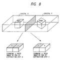
- an electron beam diffraction pattern from a specific fine region on the sample surface can be observed by narrowing the electron beam diameter of 0.1 ⁇ m. Also, by scanning the electron beam two-dimensionally on the sample surface, by use of any desired diffraction spot intensity change on the diffraction pattern as the image signal, two dimensional image (scanning ⁇ -RHEED image) on the sample surface can be obtained. At this time by observation of the scanning ⁇ -RHEED image by use of different diffraction spots A and C on the diffraction pattern as shown in Fig.
- the diffraction spot A is a diffraction spot on the line (line 1) where the plane in which the diffraction pattern occurs and the sagittal plane formed by the incident electron beam are crossed at right angle, while the diffraction spot 6 is a diffraction spot not on the line 1.
- line 1 where the plane in which the diffraction pattern occurs and the sagittal plane formed by the incident electron beam are crossed at right angle
- the diffraction spot 6 is a diffraction spot not on the line 1.
- the Al selectively deposited was found to be similarly Al (100) monocrystal. Those at substrate temperatures ranging from 250 o C to 330 o C were selectively deposited stably, and the Al obtained was found to become monocrystal.
- Al films deposited selectively on the Si (111) substrate with the Si (111) plane being at off-angles by 1 o , 2 o , 3 o , 4 o , 5 o from the Si substrate were also found to deposit Al (100) monocrystals under the temperature conditions of the substrate temperature ranging from 250 o C to 330 o C similarly as deposited on the Si (111) substrate as described above.
- Fig. 12 shows the scanning secondary electron image (Fig. 12A) and the scanning ⁇ -RHEED image (Figs. 12B and 12C) when Al was selectively deposited on only the Si exposed surface on a substrate having Si (100) exposed in a line by patterning of SiO2 in a line.
- the scanning ⁇ -RHEED image the 333 diffraction spots (Fig. 12B) and 531 diffraction spots (Fig. 12C) were employed.
- the Al film selectively deposited was confirmed to be an Al (111) monocrystal. Those at substrate temperatures ranging from 250 o C to 330 o C were found to be selectively deposited stably, and the Al films obtained became monocrystals.
- Al films deposited selectively on the Si (100) substrate with the Si (100) plane beirig at off-angles by 1 o , 2 o , 3 o , 4 o , 5 o from the Si substrate surface were also found to deposit Al (111) monocrystals under the temperature conditions of the substrate temperature ranging from 250 o C to 330 o C similarly as deposited on the Si (111) substrate as described above.
- the Al selectively deposited on Si was found to be Al (100).
- the Al film selectively deposited was found to be Al (111).
- the Al film selectively deposited on TiN was found to be oriented in Al (111) from X-ray diffraction, and from reflective high speed electron beam diffraction pattern of the prior art by use of an electron beam of an acceleration voltage of 80 kV or 100 kV, diffraction spots concerned with Al (111) were strongly observed.
- An Al film was formed on a monocrystalline silicon under the following conditions.
- Resistivity became greater by 2-fold or more than the case when hydrogen was employed.
- Al deposited only by decomposition of DMAH without use of H2 is inferior in film quality, and was unsatisfactory as the Al film for a semiconductor device.
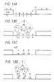
- the mechanism of Al deposition according to the present invention may be presently hypothesized as follows.
- DMAH reaches the electron donative substrate, namely the substrate having electrons under the state on which hydrogen atoms are attached (Fig. 13A) with the methyl groups directed toward the substrate side, one electron of the substrate cut one bond of Al and methyl group (Figs. 13B, 13C).
- Figs. 13A - 13D are illustrations for better understanding of the reacion mechanism, and the numbers of H, e and Al shown in Figs. 13A - 13D are not necessarily coincident.
- a low resistivity, dense and flat Al film could be deposited on a substrate.
- deposition can be effected selectively.
Landscapes
- Chemical & Material Sciences (AREA)
- General Chemical & Material Sciences (AREA)
- Chemical Kinetics & Catalysis (AREA)
- Engineering & Computer Science (AREA)
- Materials Engineering (AREA)
- Mechanical Engineering (AREA)
- Metallurgy (AREA)
- Organic Chemistry (AREA)
- Chemical Vapour Deposition (AREA)
- Electrodes Of Semiconductors (AREA)
- Internal Circuitry In Semiconductor Integrated Circuit Devices (AREA)
- Physical Vapour Deposition (AREA)
Applications Claiming Priority (8)
| Application Number | Priority Date | Filing Date | Title |
|---|---|---|---|
| JP233926/89 | 1989-09-09 | ||
| JP233924/89 | 1989-09-09 | ||
| JP23392689 | 1989-09-09 | ||
| JP23392489 | 1989-09-09 | ||
| JP6558/90 | 1990-01-16 | ||
| JP2006558A JP2781239B2 (ja) | 1989-09-09 | 1990-01-16 | 堆積膜形成法 |
| JP2006557A JP2831770B2 (ja) | 1989-09-09 | 1990-01-16 | 堆積膜形成法 |
| JP6557/90 | 1990-01-16 |
Publications (2)
| Publication Number | Publication Date |
|---|---|
| EP0425084A1 true EP0425084A1 (de) | 1991-05-02 |
| EP0425084B1 EP0425084B1 (de) | 1996-01-03 |
Family
ID=27454509
Family Applications (1)
| Application Number | Title | Priority Date | Filing Date |
|---|---|---|---|
| EP90309800A Expired - Lifetime EP0425084B1 (de) | 1989-09-09 | 1990-09-07 | Verfahren zur Abscheidung von einem Film mittels eines Alkylaluminiumhydrids |
Country Status (8)
| Country | Link |
|---|---|
| US (2) | US5179042A (de) |
| EP (1) | EP0425084B1 (de) |
| AT (1) | ATE132543T1 (de) |
| DE (1) | DE69024607T2 (de) |
| DK (1) | DK0425084T3 (de) |
| ES (1) | ES2081941T3 (de) |
| GR (1) | GR3019282T3 (de) |
| PT (1) | PT95232B (de) |
Cited By (11)
| Publication number | Priority date | Publication date | Assignee | Title |
|---|---|---|---|---|
| EP0448223A3 (en) * | 1990-02-19 | 1992-02-19 | Canon Kabushiki Kaisha | Process for forming metal deposited film containing aluminium as main component by use of alkyl aluminum hydride |
| EP0498580A1 (de) * | 1991-02-04 | 1992-08-12 | Canon Kabushiki Kaisha | Verfahren zur Herstellung einer abgeschiedenen Metallschicht, die Aluminium enthält, mit Anwendung von Alkylaluminiumhalid |
| EP0567985A3 (en) * | 1992-04-28 | 1994-05-18 | Tsubochi Kazuo | Process for thin film formation |
| US5317433A (en) * | 1991-12-02 | 1994-05-31 | Canon Kabushiki Kaisha | Image display device with a transistor on one side of insulating layer and liquid crystal on the other side |
| US5364664A (en) * | 1990-12-21 | 1994-11-15 | Canon Kabushiki Kaisha | Process for non-selectively forming deposition film on a non-electron-donative surface |
| EP0581280A3 (en) * | 1992-07-31 | 1995-12-13 | Canon Kk | Pattern forming method |
| US5476815A (en) * | 1991-05-23 | 1995-12-19 | Canon Kabushiki Kaisha | Manufacturing method of semiconductor device |
| EP0566040A3 (en) * | 1992-04-13 | 1996-01-10 | Air Prod & Chem | Process for selectively depositing copper aluminum alloy onto a substrate |
| US5633182A (en) * | 1991-12-02 | 1997-05-27 | Canon Kabushiki Kaisha | Method of manufacturing an image display device with reduced cell gap variation |
| US5776255A (en) * | 1992-12-24 | 1998-07-07 | Canon Kabushiki Kaisha | Chemical vapor deposition apparatus |
| US6309971B1 (en) * | 1996-08-01 | 2001-10-30 | Cypress Semiconductor Corporation | Hot metallization process |
Families Citing this family (30)
| Publication number | Priority date | Publication date | Assignee | Title |
|---|---|---|---|---|
| PT95232B (pt) * | 1989-09-09 | 1998-06-30 | Canon Kk | Processo de producao de uma pelicula de aluminio depositada |
| JP2721023B2 (ja) * | 1989-09-26 | 1998-03-04 | キヤノン株式会社 | 堆積膜形成法 |
| ATE150585T1 (de) * | 1990-05-31 | 1997-04-15 | Canon Kk | Verfahren zur herstellung einer halbleitervorrichtung mit einer verdrahtungsstruktur hoher dichte |
| DE69132730T2 (de) * | 1990-05-31 | 2002-07-04 | Canon K.K., Tokio/Tokyo | Halbleiteranordnung mit verbesserter Leitungsführung |
| DE69109366T2 (de) * | 1990-05-31 | 1995-10-19 | Canon Kk | Verfahren zur Herstellung einer Halbleiteranordnung mit Gatestruktur. |
| JP2895166B2 (ja) * | 1990-05-31 | 1999-05-24 | キヤノン株式会社 | 半導体装置の製造方法 |
| JP2974376B2 (ja) * | 1990-06-01 | 1999-11-10 | キヤノン株式会社 | 半導体装置の製造方法 |
| MY109605A (en) * | 1990-06-29 | 1997-03-31 | Canon Kk | Method for producing semiconductor device having alignment mark. |
| US5627345A (en) * | 1991-10-24 | 1997-05-06 | Kawasaki Steel Corporation | Multilevel interconnect structure |
| US6004885A (en) | 1991-12-26 | 1999-12-21 | Canon Kabushiki Kaisha | Thin film formation on semiconductor wafer |
| JP3222518B2 (ja) * | 1991-12-26 | 2001-10-29 | キヤノン株式会社 | 液体原料気化装置および薄膜形成装置 |
| US5447568A (en) * | 1991-12-26 | 1995-09-05 | Canon Kabushiki Kaisha | Chemical vapor deposition method and apparatus making use of liquid starting material |
| US5580808A (en) * | 1992-07-30 | 1996-12-03 | Canon Kabushiki Kaisha | Method of manufacturing a ROM device having contact holes treated with hydrogen atoms and energy beam |
| EP0608628A3 (de) * | 1992-12-25 | 1995-01-18 | Kawasaki Steel Co | Verfahren zur Herstellung einer Halbleitervorrichtung mit Mehrlagen-Verbindungsstruktur. |
| KR100320364B1 (ko) * | 1993-03-23 | 2002-04-22 | 가와사키 마이크로 엘렉트로닉스 가부시키가이샤 | 금속배선및그의형성방법 |
| US5429989A (en) * | 1994-02-03 | 1995-07-04 | Motorola, Inc. | Process for fabricating a metallization structure in a semiconductor device |
| US5565381A (en) * | 1994-08-01 | 1996-10-15 | Microchip Technology Incorporated | Method of removing sharp edges in a dielectric coating located above a semiconductor substrate and a semiconductor device formed by this method |
| JPH08148563A (ja) * | 1994-11-22 | 1996-06-07 | Nec Corp | 半導体装置の多層配線構造体の形成方法 |
| KR0161116B1 (ko) * | 1995-01-06 | 1999-02-01 | 문정환 | 반도체 장치의 금속층 형성방법 |
| US5650198A (en) * | 1995-08-18 | 1997-07-22 | The Regents Of The University Of California | Defect reduction in the growth of group III nitrides |
| JP3695606B2 (ja) * | 1996-04-01 | 2005-09-14 | 忠弘 大見 | 半導体装置及びその製造方法 |
| US5783485A (en) * | 1996-07-19 | 1998-07-21 | Motorola, Inc. | Process for fabricating a metallized interconnect |
| US6156645A (en) * | 1996-10-25 | 2000-12-05 | Cypress Semiconductor Corporation | Method of forming a metal layer on a substrate, including formation of wetting layer at a high temperature |
| US5969423A (en) * | 1997-07-15 | 1999-10-19 | Micron Technology, Inc. | Aluminum-containing films derived from using hydrogen and oxygen gas in sputter deposition |
| US6222271B1 (en) | 1997-07-15 | 2001-04-24 | Micron Technology, Inc. | Method of using hydrogen gas in sputter deposition of aluminum-containing films and aluminum-containing films derived therefrom |
| JPH11150084A (ja) | 1997-09-12 | 1999-06-02 | Canon Inc | 半導体装置および基板上への非晶質窒化硅素チタンの形成方法 |
| US6057238A (en) * | 1998-03-20 | 2000-05-02 | Micron Technology, Inc. | Method of using hydrogen and oxygen gas in sputter deposition of aluminum-containing films and aluminum-containing films derived therefrom |
| US6187673B1 (en) | 1998-09-03 | 2001-02-13 | Micron Technology, Inc. | Small grain size, conformal aluminum interconnects and method for their formation |
| US7485560B2 (en) * | 2006-11-22 | 2009-02-03 | Atomic Energy Council - Institute Of Nuclear Energy Research | Method for fabricating crystalline silicon thin films |
| US8183145B2 (en) | 2007-10-11 | 2012-05-22 | International Business Machines Corporation | Structure and methods of forming contact structures |
Citations (1)
| Publication number | Priority date | Publication date | Assignee | Title |
|---|---|---|---|---|
| DE2053242A1 (de) * | 1969-10-29 | 1971-05-06 | Sumitomo Chemical Co | Verfahren zum Belegen eines Substrats mit Aluminium |
Family Cites Families (8)
| Publication number | Priority date | Publication date | Assignee | Title |
|---|---|---|---|---|
| GB2038883B (en) * | 1978-11-09 | 1982-12-08 | Standard Telephones Cables Ltd | Metallizing semiconductor devices |
| JP2559030B2 (ja) * | 1986-07-25 | 1996-11-27 | 日本電信電話株式会社 | 金属薄膜の製造方法 |
| JPH01252776A (ja) * | 1988-03-31 | 1989-10-09 | Sony Corp | 気相成長アルミニウム膜形成方法 |
| JP2570839B2 (ja) * | 1988-12-22 | 1997-01-16 | 日本電気株式会社 | A▲l▼ーCu合金薄膜形成方法 |
| JPH02185026A (ja) * | 1989-01-11 | 1990-07-19 | Nec Corp | Al薄膜の選択的形成方法 |
| PT95232B (pt) * | 1989-09-09 | 1998-06-30 | Canon Kk | Processo de producao de uma pelicula de aluminio depositada |
| US5217756A (en) * | 1990-06-08 | 1993-06-08 | Nec Corporation | Selective chemical vapor deposition of aluminum, aluminum CVD materials and process for preparing the same |
| DE69130595T2 (de) * | 1990-07-06 | 1999-05-27 | Tsubouchi, Kazuo, Sendai, Miyagi | Verfahren zur Herstellung einer Metallschicht |
-
1990
- 1990-09-06 PT PT95232A patent/PT95232B/pt not_active IP Right Cessation
- 1990-09-07 ES ES90309800T patent/ES2081941T3/es not_active Expired - Lifetime
- 1990-09-07 US US07/578,672 patent/US5179042A/en not_active Expired - Lifetime
- 1990-09-07 DE DE69024607T patent/DE69024607T2/de not_active Expired - Fee Related
- 1990-09-07 DK DK90309800.2T patent/DK0425084T3/da active
- 1990-09-07 AT AT90309800T patent/ATE132543T1/de not_active IP Right Cessation
- 1990-09-07 EP EP90309800A patent/EP0425084B1/de not_active Expired - Lifetime
-
1992
- 1992-06-23 US US07/902,829 patent/US5328873A/en not_active Expired - Lifetime
-
1996
- 1996-03-12 GR GR960400685T patent/GR3019282T3/el unknown
Patent Citations (1)
| Publication number | Priority date | Publication date | Assignee | Title |
|---|---|---|---|---|
| DE2053242A1 (de) * | 1969-10-29 | 1971-05-06 | Sumitomo Chemical Co | Verfahren zum Belegen eines Substrats mit Aluminium |
Non-Patent Citations (4)
| Title |
|---|
| APPLIED PHYSICS LETTERS, vol. 52, no. 22, 30th May 1988, pages 1865-1867, New York, US; T. CACOURIS et al.: "Laser direct writing of aluminum conductors" * |
| APPLIED PHYSICS LETTERS, vol. 55, no. 8, 21st August 1989, pages 741-743, New York, US; C. SASAOKA et al.: "Aluminum selective area deposition on Si using diethylaluminumchloride" * |
| JAPANESE JOURNAL OF APPLIED PHYSICS, part 2: letters, vol. 27, no. 8, August 1988, pages L1392-L1394, Tokyo, JP; M. HANABUSA et al.: "Photochemical vapor deposition of aluminum thin films using dimethylaluminum hydride" * |
| THIN SOLID FILMS, vol. 45, 1977, pages 257-263, Lausanne, CH; H.O. PIERSON: "Aluminum coatings by the decomposition of alkyls" * |
Cited By (19)
| Publication number | Priority date | Publication date | Assignee | Title |
|---|---|---|---|---|
| US5151305A (en) * | 1990-02-19 | 1992-09-29 | Canon Kabushiki Kaisha | Process for forming metal deposited film containing aluminum as main component by use of alkyl aluminum hydride |
| US6258174B1 (en) | 1990-02-19 | 2001-07-10 | Canon Kabushiki Kaisha | Gas supplying apparatus |
| EP0448223A3 (en) * | 1990-02-19 | 1992-02-19 | Canon Kabushiki Kaisha | Process for forming metal deposited film containing aluminium as main component by use of alkyl aluminum hydride |
| US5330633A (en) * | 1990-02-19 | 1994-07-19 | Canon Kabushiki Kaisha | Process for forming metal deposited film containing aluminum as main component by use of alkyl aluminum hydride |
| US5364664A (en) * | 1990-12-21 | 1994-11-15 | Canon Kabushiki Kaisha | Process for non-selectively forming deposition film on a non-electron-donative surface |
| EP0493002B1 (de) * | 1990-12-21 | 1996-09-11 | Kazuo Tsubouchi | Verfahren zur Herstellung eines aufgedampften Films |
| US5492734A (en) * | 1991-02-04 | 1996-02-20 | Canon Kabushiki Kaisha | Method of forming deposition film |
| EP0498580A1 (de) * | 1991-02-04 | 1992-08-12 | Canon Kabushiki Kaisha | Verfahren zur Herstellung einer abgeschiedenen Metallschicht, die Aluminium enthält, mit Anwendung von Alkylaluminiumhalid |
| US5476815A (en) * | 1991-05-23 | 1995-12-19 | Canon Kabushiki Kaisha | Manufacturing method of semiconductor device |
| US5317433A (en) * | 1991-12-02 | 1994-05-31 | Canon Kabushiki Kaisha | Image display device with a transistor on one side of insulating layer and liquid crystal on the other side |
| US5633182A (en) * | 1991-12-02 | 1997-05-27 | Canon Kabushiki Kaisha | Method of manufacturing an image display device with reduced cell gap variation |
| EP0566040A3 (en) * | 1992-04-13 | 1996-01-10 | Air Prod & Chem | Process for selectively depositing copper aluminum alloy onto a substrate |
| US5604153A (en) * | 1992-04-28 | 1997-02-18 | Tsubouchi; Kazuo | Process for thin film formation |
| EP0567985A3 (en) * | 1992-04-28 | 1994-05-18 | Tsubochi Kazuo | Process for thin film formation |
| EP0581280A3 (en) * | 1992-07-31 | 1995-12-13 | Canon Kk | Pattern forming method |
| US5861233A (en) * | 1992-07-31 | 1999-01-19 | Canon Kabushiki Kaisha | Pattern forming method by imparting hydrogen atoms and selectively depositing metal film |
| US5776255A (en) * | 1992-12-24 | 1998-07-07 | Canon Kabushiki Kaisha | Chemical vapor deposition apparatus |
| US6309971B1 (en) * | 1996-08-01 | 2001-10-30 | Cypress Semiconductor Corporation | Hot metallization process |
| US6627547B2 (en) | 1996-08-01 | 2003-09-30 | Cypress Semiconductor Corporation | Hot metallization process |
Also Published As
| Publication number | Publication date |
|---|---|
| DK0425084T3 (da) | 1996-01-29 |
| PT95232A (pt) | 1991-05-22 |
| ES2081941T3 (es) | 1996-03-16 |
| ATE132543T1 (de) | 1996-01-15 |
| US5328873A (en) | 1994-07-12 |
| DE69024607D1 (de) | 1996-02-15 |
| GR3019282T3 (en) | 1996-06-30 |
| DE69024607T2 (de) | 1996-06-13 |
| PT95232B (pt) | 1998-06-30 |
| US5179042A (en) | 1993-01-12 |
| EP0425084B1 (de) | 1996-01-03 |
Similar Documents
| Publication | Publication Date | Title |
|---|---|---|
| EP0425084B1 (de) | Verfahren zur Abscheidung von einem Film mittels eines Alkylaluminiumhydrids | |
| EP0420595B1 (de) | Herstellen von einer selektiv niedergeschlagenen Schicht mit Anwendung von Alkylaluminiumhydrid | |
| EP0420594B1 (de) | Verfahren zur Herstellung von einer abgeschiedenen Metallschicht, die Aluminium als Hauptkomponent enthält, mit Anwendung von Alkalimetallaluminiumhydride | |
| US4897709A (en) | Titanium nitride film in contact hole with large aspect ratio | |
| US7172968B2 (en) | Ultra thin, single phase, diffusion barrier for metal conductors | |
| EP0407133B1 (de) | Halbleitervorrichtung und Verfahren zu deren Herstellung | |
| US4902645A (en) | Method of selectively forming a silicon-containing metal layer | |
| US6458684B1 (en) | Single step process for blanket-selective CVD aluminum deposition | |
| EP1077486B1 (de) | Halbleitervorrichtung | |
| EP0420597B1 (de) | Verfahren zur Herstellung einer abgeschiedenen Schicht unter Verwendung von Alkylaluminiumhydrid und Verfahren zur Herstellung eines Halbleiterbauelements | |
| US6066358A (en) | Blanket-selective chemical vapor deposition using an ultra-thin nucleation layer | |
| EP0425090B1 (de) | Verfahren und Vorrichtung zur Abscheidung einer Schicht | |
| US6156647A (en) | Barrier layer structure which prevents migration of silicon into an adjacent metallic layer and the method of fabrication of the barrier layer | |
| US6887353B1 (en) | Tailored barrier layer which provides improved copper interconnect electromigration resistance | |
| EP0420589B1 (de) | Verfahren zum Herstellen einer abgeschiedenen Schicht und Verfahren zum Herstellen einer Halbleitervorrichtung | |
| EP0417997B1 (de) | Verfahren zur Abscheidung von einem Aluminium als Hauptbestandteil enthaltenden metallischen Film mittels eines Alkylaluminiumhydrids | |
| JP2721013B2 (ja) | 堆積膜形成法 | |
| JP2781239B2 (ja) | 堆積膜形成法 | |
| KR940011005B1 (ko) | 알킬 알루미늄 하이드라이드를 이용한 퇴적막 형성법 | |
| JP2831770B2 (ja) | 堆積膜形成法 | |
| JP2670152B2 (ja) | 堆積膜形成法 | |
| JP2781219B2 (ja) | 堆積膜形成法 | |
| JP2721021B2 (ja) | 堆積膜形成法 | |
| JP2670151B2 (ja) | 堆積膜形成法 | |
| JP2834788B2 (ja) | 堆積膜形成法 |
Legal Events
| Date | Code | Title | Description |
|---|---|---|---|
| PUAI | Public reference made under article 153(3) epc to a published international application that has entered the european phase |
Free format text: ORIGINAL CODE: 0009012 |
|
| 17P | Request for examination filed |
Effective date: 19901231 |
|
| AK | Designated contracting states |
Kind code of ref document: A1 Designated state(s): AT BE CH DE DK ES FR GB GR IT LI LU NL SE |
|
| 17Q | First examination report despatched |
Effective date: 19930608 |
|
| GRAA | (expected) grant |
Free format text: ORIGINAL CODE: 0009210 |
|
| AK | Designated contracting states |
Kind code of ref document: B1 Designated state(s): AT BE CH DE DK ES FR GB GR IT LI LU NL SE |
|
| REF | Corresponds to: |
Ref document number: 132543 Country of ref document: AT Date of ref document: 19960115 Kind code of ref document: T |
|
| ITF | It: translation for a ep patent filed | ||
| REG | Reference to a national code |
Ref country code: DK Ref legal event code: T3 |
|
| REF | Corresponds to: |
Ref document number: 69024607 Country of ref document: DE Date of ref document: 19960215 |
|
| REG | Reference to a national code |
Ref country code: CH Ref legal event code: NV Representative=s name: BOVARD AG PATENTANWAELTE |
|
| REG | Reference to a national code |
Ref country code: ES Ref legal event code: FG2A Ref document number: 2081941 Country of ref document: ES Kind code of ref document: T3 |
|
| ET | Fr: translation filed | ||
| REG | Reference to a national code |
Ref country code: GR Ref legal event code: FG4A Free format text: 3019282 |
|
| PLBE | No opposition filed within time limit |
Free format text: ORIGINAL CODE: 0009261 |
|
| STAA | Information on the status of an ep patent application or granted ep patent |
Free format text: STATUS: NO OPPOSITION FILED WITHIN TIME LIMIT |
|
| 26N | No opposition filed | ||
| REG | Reference to a national code |
Ref country code: GB Ref legal event code: IF02 |
|
| PGFP | Annual fee paid to national office [announced via postgrant information from national office to epo] |
Ref country code: ES Payment date: 20080806 Year of fee payment: 19 Ref country code: DK Payment date: 20080904 Year of fee payment: 19 Ref country code: LU Payment date: 20080911 Year of fee payment: 19 Ref country code: CH Payment date: 20080904 Year of fee payment: 19 |
|
| PGFP | Annual fee paid to national office [announced via postgrant information from national office to epo] |
Ref country code: NL Payment date: 20080915 Year of fee payment: 19 Ref country code: IT Payment date: 20080918 Year of fee payment: 19 Ref country code: AT Payment date: 20080909 Year of fee payment: 19 |
|
| PGFP | Annual fee paid to national office [announced via postgrant information from national office to epo] |
Ref country code: GB Payment date: 20080911 Year of fee payment: 19 |
|
| PGFP | Annual fee paid to national office [announced via postgrant information from national office to epo] |
Ref country code: DE Payment date: 20080930 Year of fee payment: 19 |
|
| PGFP | Annual fee paid to national office [announced via postgrant information from national office to epo] |
Ref country code: SE Payment date: 20080904 Year of fee payment: 19 Ref country code: BE Payment date: 20080901 Year of fee payment: 19 |
|
| PGFP | Annual fee paid to national office [announced via postgrant information from national office to epo] |
Ref country code: FR Payment date: 20080923 Year of fee payment: 19 |
|
| PGFP | Annual fee paid to national office [announced via postgrant information from national office to epo] |
Ref country code: GR Payment date: 20080902 Year of fee payment: 19 |
|
| BERE | Be: lapsed |
Owner name: *CANON K.K. Effective date: 20090930 |
|
| REG | Reference to a national code |
Ref country code: NL Ref legal event code: V1 Effective date: 20100401 |
|
| REG | Reference to a national code |
Ref country code: CH Ref legal event code: PL |
|
| EUG | Se: european patent has lapsed | ||
| REG | Reference to a national code |
Ref country code: DK Ref legal event code: EBP |
|
| GBPC | Gb: european patent ceased through non-payment of renewal fee |
Effective date: 20090907 |
|
| REG | Reference to a national code |
Ref country code: FR Ref legal event code: ST Effective date: 20100531 |
|
| PG25 | Lapsed in a contracting state [announced via postgrant information from national office to epo] |
Ref country code: AT Free format text: LAPSE BECAUSE OF NON-PAYMENT OF DUE FEES Effective date: 20090907 |
|
| PG25 | Lapsed in a contracting state [announced via postgrant information from national office to epo] |
Ref country code: NL Free format text: LAPSE BECAUSE OF NON-PAYMENT OF DUE FEES Effective date: 20100401 Ref country code: DE Free format text: LAPSE BECAUSE OF NON-PAYMENT OF DUE FEES Effective date: 20100401 Ref country code: FR Free format text: LAPSE BECAUSE OF NON-PAYMENT OF DUE FEES Effective date: 20090930 |
|
| PG25 | Lapsed in a contracting state [announced via postgrant information from national office to epo] |
Ref country code: BE Free format text: LAPSE BECAUSE OF NON-PAYMENT OF DUE FEES Effective date: 20090930 |
|
| PG25 | Lapsed in a contracting state [announced via postgrant information from national office to epo] |
Ref country code: GR Free format text: LAPSE BECAUSE OF NON-PAYMENT OF DUE FEES Effective date: 20100406 Ref country code: CH Free format text: LAPSE BECAUSE OF NON-PAYMENT OF DUE FEES Effective date: 20090930 Ref country code: LI Free format text: LAPSE BECAUSE OF NON-PAYMENT OF DUE FEES Effective date: 20090930 |
|
| PG25 | Lapsed in a contracting state [announced via postgrant information from national office to epo] |
Ref country code: GB Free format text: LAPSE BECAUSE OF NON-PAYMENT OF DUE FEES Effective date: 20090907 |
|
| PG25 | Lapsed in a contracting state [announced via postgrant information from national office to epo] |
Ref country code: DK Free format text: LAPSE BECAUSE OF NON-PAYMENT OF DUE FEES Effective date: 20090930 |
|
| REG | Reference to a national code |
Ref country code: ES Ref legal event code: FD2A Effective date: 20110224 |
|
| PG25 | Lapsed in a contracting state [announced via postgrant information from national office to epo] |
Ref country code: IT Free format text: LAPSE BECAUSE OF NON-PAYMENT OF DUE FEES Effective date: 20090907 |
|
| PG25 | Lapsed in a contracting state [announced via postgrant information from national office to epo] |
Ref country code: LU Free format text: LAPSE BECAUSE OF NON-PAYMENT OF DUE FEES Effective date: 20090907 |
|
| PG25 | Lapsed in a contracting state [announced via postgrant information from national office to epo] |
Ref country code: SE Free format text: LAPSE BECAUSE OF NON-PAYMENT OF DUE FEES Effective date: 20090908 |
|
| PG25 | Lapsed in a contracting state [announced via postgrant information from national office to epo] |
Ref country code: ES Free format text: LAPSE BECAUSE OF NON-PAYMENT OF DUE FEES Effective date: 20090908 |